Magnetic Proximity induced efficient charge-to-spin conversion in large area PtSe2/Ni80Fe20 heterostructures
Abstract
As a topological Dirac semimetal with controllable spin-orbit coupling and conductivity, PtSe2, a transition-metal dichalcogenide, is a promising material for several applications from optoelectric to sensors. However, its potential for spintronics applications is yet to be explored. In this work, we demonstrate that PtSe2/Ni80Fe20 heterostructure can generate a large damping-like current-induced spin-orbit torques (SOT), despite the absence of spin-splitting in bulk PtSe2. The efficiency of charge-to-spin conversion is found to be nm-1 in PtSe2/Ni80Fe20, which is three times that of the control sample, Ni80Fe20/Pt. Our band structure calculations show that the SOT due to the PtSe2 arises from an unexpectedly large spin splitting in the interfacial region of PtSe2 introduced by the proximity magnetic field of the Ni80Fe20 layer. Our results open up the possibilities of using large-area PtSe2 for energy-efficient nanoscale devices by utilizing the proximity-induced SOT.
Indian Institute of Technology Delhi] Department of Physics, Indian Institute of Technology Delhi, Hauz Khas, New Delhi-110016, India Indian Institute of Technology Delhi] Center for Applied Research in Electronics, Indian Institute of Technology Delhi, Hauz Khas, New Delhi-110016, India Indian Institute of Technology Delhi] Department of Physics, Indian Institute of Technology Delhi, Hauz Khas, New Delhi-110016, India Indian Institute of Technology Delhi] Department of Physics, Indian Institute of Technology Delhi, Hauz Khas, New Delhi-110016, India Indian Institute of Technology Madras] Condensed Matter Theory and Computational Lab, Department of Physics, Indian Institute of Technology Madras, Chennai 600036, India \alsoaffiliation[Indian Institute of Technology Madras] Center for Atomistic Modelling and Materials Design, Indian Institute of Technology Madras, Chennai 600036, India Indian Institute of Technology Madras] Condensed Matter Theory and Computational Lab, Department of Physics, Indian Institute of Technology Madras, Chennai 600036, India \alsoaffiliationDepartment of Physics & Astronomy, University of Missouri, Columbia, MO 65211, USA Indian Institute of Technology Delhi] Department of Physics, Indian Institute of Technology Delhi, Hauz Khas, New Delhi-110016, India Indian Institute of Technology Delhi] Department of Physics, Indian Institute of Technology Delhi, Hauz Khas, New Delhi-110016, India \alsoaffiliation[University of Gothenburg] Department of Physics, University of Gothenburg, Gothenburg-412 96, Sweden Indian Institute of Technology Delhi] Department of Physics, Indian Institute of Technology Delhi, Hauz Khas, New Delhi-110016, India Saha Institute of Nuclear Physics]Surface Physics & Material Science Division, Saha Institute of Nuclear Physics, A CI of Homi Bhabha National Institute, 1/AF Bidhannagar, Kolkata 700064, India Indian Institute of Technology Madras] Condensed Matter Theory and Computational Lab, Department of Physics, Indian Institute of Technology Madras, Chennai 600036, India \alsoaffiliation[Indian Institute of Technology Madras] Center for Atomistic Modelling and Materials Design, Indian Institute of Technology Madras, Chennai 600036, India Indian Institute of Technology Madras] Condensed Matter Theory and Computational Lab, Department of Physics, Indian Institute of Technology Madras, Chennai 600036, India \alsoaffiliationDepartment of Physics & Astronomy, University of Missouri, Columbia, MO 65211, USA \alsoaffiliation[Indian Institute of Technology Madras] Center for Atomistic Modelling and Materials Design, Indian Institute of Technology Madras, Chennai 600036, India Indian Institute of Technology Delhi] Center for Applied Research in Electronics, Indian Institute of Technology Delhi, Hauz Khas, New Delhi-110016, India Indian Institute of Technology Delhi] Department of Physics, Indian Institute of Technology Delhi, Hauz Khas, New Delhi-110016, India
The next generation of spintronic memories can be realized using spin-orbit torques (SOT), an energy-efficient and faster way to manipulate magnetization. 1 In ferromagnet (FM)/heavy metal (HM) bilayers, SOT describes the current-induced torque exerted on the FM layer. The flow of a charge current in an FM/HM system can generate a spin current, transverse to the direction of charge current flow, by mechanisms such as the spin Hall effect, 2 or Rashba-Edelstein. 3 Typically heavy metals, such as Pt, 4, 5 W, 6, 7, 5 and Ta 8, 9 are used to generate spin currents. Significant efforts have been reported to improve the energy efficiency of HM-based SOT devices. 10, 11, 12 One method to achieve a higher SOT efficiency is by replacing the HM layer with alternative materials that have large charge-to-spin conversion efficiency and high conductivity. Transition metal dichalcogenides (TMDs) are potential replacements of HM due to various properties such as tunable conductivity, 13, 14 high spin–orbit coupling, 15, 16, 17 the presence of Dzyaloshinskii Moriya-interaction, 18 tunable band structure, 19, 20 spin-layer locking 21 and long spin-life time. 22 The use of TMDs in SOT devices has shown a number of advantages, e.g., the ability to control SOT using the crystal symmetry 23, 24, 25 and electric field. 26
The Pt-based TMDs offer advantages such as high air stability,27, and large spin-orbit coupling. 28 However, SOT studies on Pt-based TMDs have been limited to PtTe2 for which a recent work showed a large damping-like torque and SOT switching. 29 PtSe2 is another Pt-based TMD offering high and tunable spin-orbit coupling. 28 It is also a type-II Dirac semi-metal, offering several topologically protected phenomena potentially useful for spintronic applications. 30 In addition, the band structure of PtSe2 exhibits topological surface states, 31 which can be exploited for topological spintronic devices. It has been demonstrated that the monolayer PtSe2 film possesses spin-layer locking 21 with many interesting electronic properties. 32 These intriguing properties suggest that PtSe2 might be a promising candidate for investigating the SOT phenomenon. However, unlike other TMDs 17, the band structure of PtSe2 does not show spin splitting. In addition, the type II Dirac cone appears much below the Fermi energy in the bulk PtSe2. 30
In this work, we investigate SOT in PtSe2/Ni80Fe20(or NiFe)/Pt heterostructures using the spin torque ferromagnetic resonance (STFMR) technique. We found a large increase in the effective damping constant (164%) in PtSe2/NiFe/Pt compared to the NiFe/Pt control sample. Using angle-resolved STFMR measurements, we demonstrated that only conventional SOTs are generated in PtSe2/NiFe/Pt, with spin polarization along the y-axis for a charge current flowing along the x-direction, which is in accordance with theoretical predictions. 33 From the line shape analysis, we determine an enhanced effective damping-like torque due to PtSe2. We found a maximum interfacial charge-to-spin conversion efficiency of nm-1 due to PtSe2. Our band structure calculation of PtSe2 that includes the proximity of the FM layer shows that NiFe introduces: (a) charge transfer from NiFe to PtSe2, (b) a Rashba SOC due to the surface symmetry breaking, and (c) a proximity magnetic field induced spin-splitting that could lead to enhanced spin Hall conductivity (SHC) in the interface region. The enhanced SOT due to PtSe2 is qualitatively explained using the substantial spin splitting introduced by the proximity magnetic field.
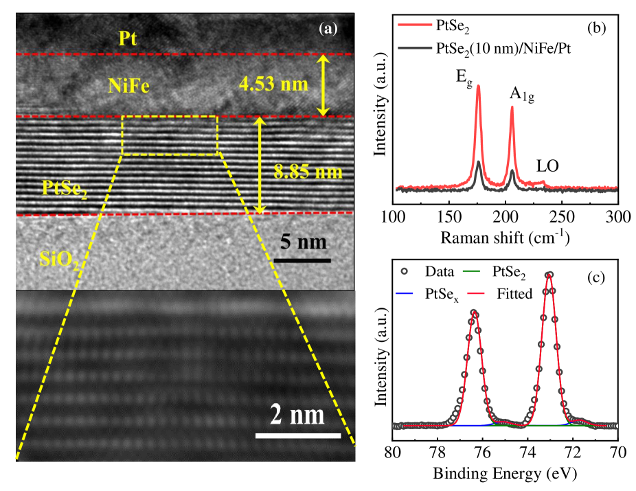
We used a thermally assisted conversion process to grow large-area PtSe2 thin films. 34 HRTEM and XRD (section S1 in supplementary) measurements on PtSe2 show the growth of crystalline films. Figure 1 (a) shows the cross-sectional HRTEM image of PtSe2/NiFe/Pt stack. The image shows that the whole Pt layer gets selenized, and a high-quality PtSe2 lattice with a 1T structure is formed. The thickness of PtSe2 is found 9 nm, and the separation between two consecutive layers is 0.5 nm. Each layer corresponds to a monolayer of PtSe2, which contains one Pt layer sandwiched between two Se layers. A magnified view of the square region is shown at the bottom of the figure. Based on HRTEM and AFM measurements (Section S1 in supplementary), we determine the thickness of PtSe2 after selenization of 3 nm thick Pt to be (10 1.0) nm. This increase in the thickness of Pt due to its selenization is well-known in the literature, 35 and it further confirms the complete selenization of the Pt layer. Figure 1 (b) shows the Raman spectra of PtSe2, measured with a laser of wavelength 532 nm. The spectrum contains two distinct peaks that corresponds to PtSe2: Eg at 176 cm-1 and A1g at 206 cm-1. Here, the Eg corresponds to the in-plane vibrations of Se atoms moving away from each other while the A1g corresponds to out-of-plane vibrations of Se atoms moving in the opposite directions. 36 A small peak labeled as longitudinal optical (LO) mode is also observed at 233 cm-1, which is a combination of in-plane and out-of-plane vibrations of Pt and Se atoms. 36, 37 The position and intensity ratio of A1g and Eg peaks confirm the presence of PtSe2 in bulk form. 36 Similar spectra were obtained at multiple locations on the sample with a ratio of the intensity of A1g and Eg peaks nearly identical (0.75 0.02), confirming the formation of a large-area homogeneous thin film of PtSe2. The chemical composition of PtSe2 was verified further by X-ray photoelectron spectroscopy (XPS). Figure 1 (c) shows the Pt-4f core-level spectra. The binding energies of the different core levels have been calibrated using the C-1s peak and the core-level spectra have been best fitted with Gaussian profiles. Peaks corresponding to IV valency of Pt are observed at 76.3 and 73 eV, while peaks centered at 75.1 and 71.8 eV show the presence of PtSex phase in a small amount. The splitting between doublet for each phase is found to be 3.3 eV, consistent with literature 38.
Subsequently, we fabricated microstrip (m2) devices for STFMR measurements using maskless lithography and lift-off method in two levels. To confirm the presence of PtSe2 after deposition of NiFe/Pt and device fabrication, we perform Raman measurements [Fig. 1 (b)] by focusing the laser on the microstrip. The intensity ratio of A1g and Eg was found to be similar compared to pure PtSe2, indicating that the quality of PtSe2 was not affected by the deposition of NiFe/Pt and our fabrication steps. The overall reduction in the intensity of the peaks is due to the finite thickness of the top metal layers.
Figure 2 (a) depicts a schematic representation of the sample stack used for STFMR experiments, while Fig. 2 (b) shows the schematic of the STFMR circuit. 11 An amplitude-modulated radio frequency (RF) current, is applied to the device through the RF port of a bias-tee. The DC port of the bias-tee is used for both measuring the rectified mixing voltage using a lock-in amplifier and applying DC current. We vary the in-plane field angle, with respect to RF current, as defined in the zoomed-in image of Fig. 2 (b).
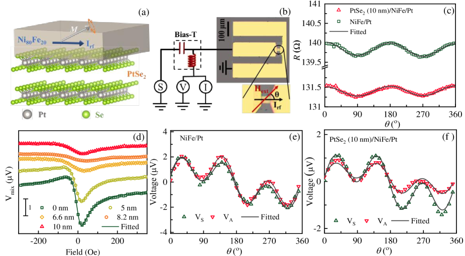
Figure 2 (c) shows the measured anisotropic magnetoresistance (AMR) of PtSe2 (10 nm)/NiFe (5 nm)/Pt (3 nm) to gather with control sample NiFe (5 nm)/Pt (3 nm). The solid lines are calculated AMR curve with , where denotes the resistance for and denotes the resistance for . The percentage of AMR, i.e., is found to be 0.19% for PtSe2/NiFe/Pt and 0.24% for NiFe/Pt. Using a parallel resistor model, we estimate that the resistance of PtSe2 to be and the resistivity to be cm. Figure 2 (d) shows the STFMR spectra for PtSe2/NiFe/Pt to gather with the control sample NiFe/Pt measured at 5 GHz with a magnetic field applied at an angle of for various thickness of PtSe2. The data for other frequencies can be found in supplementary Sec. S2. The lineshape of STFMR spectra for PtSe2/NiFe/Pt is found to be more symmetric compared to the control sample. The measured STFMR spectra can be fitted using the following equation: 4, 11
| (1) |
where, is the applied magnetic field, is the linewidth, is the resonance field, and and are the amplitudes of the symmetric and antisymmetric voltage components, respectively. By fitting the measured with above equation, we determine , , and . First, we performed angular-dependent STFMR measurements to determine the spin polarization of the interface-generated spin current. The angular dependence of and is depicted in Fig. 2 (e) and (f) for NiFe/Pt and PtSe2( 10 nm)/NiFe/Pt respectively, which follows the conventional dependence (solid lines), showing that the spin-polarization is along axis, for a charge current along the axis, which is similar to Pt and other heavy metals. 4, 23. Next, we determine the Gilbert damping constant, by fitting the versus frequency data [Fig. 3 (a)] using:4, 11
| (2) |
Here, is the gyromagnetic ratio, and is inhomogeneous linewidth which depends on magnetic inhomogeneity. The extracted value of was plotted with the thickness of PtSe2 () in the inset of Fig. 3 (a). The value of increases and becomes nearly constant for nm. The average value of for nm is (0.045 0.007), which is 165% higher than the control sample. From this, we determine spin mixing conductance to be , which is higher than other TMD/NiFe systems. 17, 16 The inhomogeneous linewidth, is found to be similar for all the devices (5 3) Oe, indicating no significant degradation in the quality of magnetic layer (NiFe) grown on PtSe2. Furthermore, the linear behavior of linewidth with frequency indicates the absence of two-magnon scattering. 39 We calculate for different stacks by fitting the behavior of the frequency versus resonance field [Fig. 3 (b)] with the Kittel formula:
| (3) |
Here, and are the anisotropy field and effective magnetization of the FM layer, respectively. By fitting the experimental data with the above equation, we found decreases with the thickness of PtSe2 as shown in the inset of Fig. 3(b). The effective magnetization is given by , where is the surface anisotropy constant, is the thickness of the FM layer, and is the saturation magnetization. Since is proportional to interfacial spin-orbit coupling, we believe the decrease of for PtSe2/NiFe/Pt is caused by the increase in interfacial spin-orbit coupling due to d-d hybridization, similar to previous reports for other TMD/FM systems. 40, 41
As stated previously, PtSe2 has a resistance greater than ; therefore, the current flowing through the PtSe2 layer is only 6% of the total current. Consequently, we anticipate SOT arising from (i) the interface between PtSe2 and NiFe and (ii) the spin Hall effect of the Pt capping. Here, we neglect self-induced torque in NiFe, which is normally one order of magnitude lower. 42 In order to quantify charge-to-spin conversion due to PtSe2, we have used line shape analysis. In this method, the SOT efficiency, is expressed as: 4
| (4) |
Here, is the electronic charge, and is the reduced Planck’s constant. Here, is the thickness of the non-magnetic layer. The above expression is valid when the field-like torque is negligible. In our case, we determined field-like torque from the anti-symmetric component of as discussed in the supplementary Sec. S4. We found field-like torque to be negligible for both NiFe/Pt and PtSe2/NiFe/Pt. However, the above equation is normally used for the case of FM/NM bilayer samples. For the trilayer system of PtSe2/NiFe/Pt, the lineshape method represents an effective spin-orbit torque efficiency, . 43 Since the conductivity of PtSe2, is much lower than that of Pt, we assume that the Oersted field is only due to the Pt layer. With these assumptions, we determine , which includes the contribution of the top Pt layer and the interfacial contribution of PtSe2.
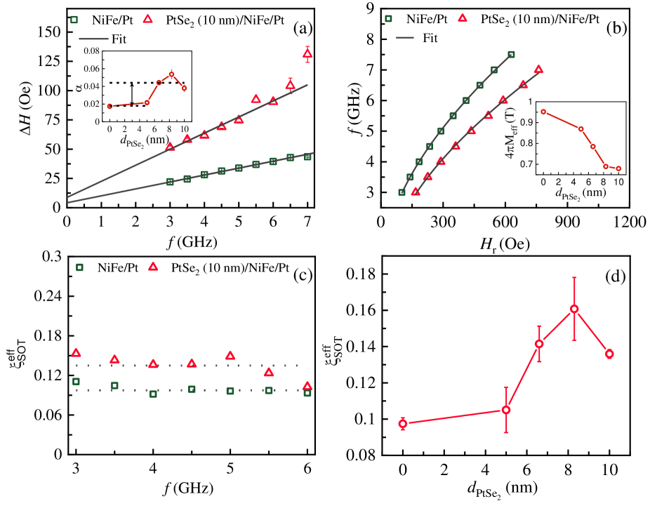
For this case, we use the thickness of Pt for in Eq. 4. 43. In Fig 3 (c), the value of has been plotted with frequency. The average value of was further calculated and plotted in Fig. 3 (d) for different thicknesses of PtSe2. The value of for 5 nm, was found to be very close to the control sample, but it increases upto for higher thickness. The value of is constant with nm. We also performed dc Planar Hall effect measurements by fabricating Hall bars. These measurements also show a similar increase of damping-like torque as discussed in supplementary material Sec. S5. The increase of due to the presence of PtSe2 indicates that the sign of spin current due to PtSe2 is opposite to that of the Pt layer. In order to extract the contribution of PtSe2, we use the symmetric and asymmetric part of the of the control sample (see supplementary Sec. S3), which also eliminates SOT from the Pt cap layer [mechanisms (ii) mentioned above]. Considering the interfacial effect as the origin of SOT, we extract the interfacial charge-to-spin conversion () following Kondou et al. 44 Here, is defined as 3D spin current () per unit 2D charge current (). The maximum interfacial charge-to-spin conversion due to PtSe2 () is determined to be nm-1. For the control samples, the interfacial charge-to-spin conversion is nm-1. Thus the magnitude of interfacial charge-to-spin conversion is nearly three times larger compared to Pt. of PtSe2 is also higher compared to that of PtTe2. 29. In this reference, the authors reported spin Hall angle/damping-like torque. Since we report an interfacial damping-like SOT, the efficiency of PtTe2-work needs to be divided by the thickness of PtTe2 for comparison with our work. Accordingly, the of PtTe2-work is nm-1, which is lower than our study. value for PtSe2 is also found to be higher compared to W, ( nm-1) 45 Bi2Te3,( nm-1) 45 and PtTe2( nm-1) 29 but it is lower than sputtered BixSe1-x thin films 46 and comparable to Ta ( nm-1). 45
The spin degeneracy in bulk PtSe2 band structure is protected due to the presence of both inversion and time-reversal symmetries. 21 Hence, the Rashba-Edelstein effect can be ruled out as the cause of SOT. In such cases, the origin of SOT by the interface is not very clear. Another possibility is that NiFe at the interface with PtSe2 is playing a crucial role in generating SOT. In order to understand the mechanism in detail, we have performed a series of ab-initio calculations using density-functional theory (DFT). The results show that NiFe introduces three things: (a) Charge transfer from NiFe to PtSe2, (b) A Rashba SOC due to the surface symmetry breaking, and (c) A proximity magnetic field that could lead to enhanced SHC in the interface region.
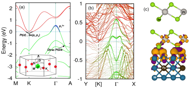
Monolayer PtSe2 is semi-conducting, and the gap closes for (PtSe, when the number of monolayers , with the band structure tending towards that of the bulk, with electron and hole pockets as indicated in Fig. 4 (a). In the (PtSeNiFe in Fig. 4 (b), we can clearly identify the bulk-like PtSe2 bands intermixed with the NiFe bands running around the gap region. We find a significant electron transfer to the interface PtSe2 layers from NiFe (), consistent with the charge density difference contours shown in Fig. 4 (c), suggesting an enhanced conductivity as well as spin splitting of the PtSe2 band structure near the interface.
A potential mechanism for spin accumulation is the Rashba-Edelstein effect (REE) due to the symmetry breaking at the interface. It is difficult to compute the Rashba SOC parameter from the PtSeNiFe calculations due to the intermixing of the NiFe bands. We have instead estimated it for the simpler case (PtSeNi, where the four monolayers are enough to reproduce the bulk band structure, and a single Ni overlayer, representing NiFe, provides the symmetry breaking. For the top-most valence band at , which represents the hole pocket in bulk PtSe2, we find eV.Å (see Fig. S6 of supplementary materials), which is rather small. However, it has been estimated that PtSe2 has a rather large momentum relaxation time fs 47. This leads to the Rashba-Edelstein length for the spin-charge conversion efficiency to be Å. This relatively low efficiency would be further reduced due to the proximity magnetic field, which tends to align the spin moments out of the plane, thereby reducing the REE. This suggests that the REE might play some role but is not a dominant mechanism for the spin accumulation at the interface. The type II Dirac cone in bulk PtSe2 is also not expected to affect spin accumulation since it occurs well below the Fermi energy.
Due to the NiFe slab, the interface PtSe2 layers will experience a proximity magnetic field, which could affect spin transport. Even though the PtSe2 layers acquire very little magnetization ( for the first and for the second layer PtSe2, compared to for Ni), there is a substantial spin-splitting of the PtSe2 band structure due to the presence of NiFe. We have estimated this value to be eV for the PtSe2 states near (see Fig. S7 of supplementary materials). This is significant and could lead to a large enhancement of the spin Hall conductivity (SHC). In fact, for the PtNiFe interface, earlier calculations by Kelly and coworkers48 have revealed that the SHC for the Pt interface layers adjacent to the NiFe is enhanced by a factor of approximately twenty-five as compared to the Pt bulk layers. This suggests that the proximity magnetic field in the interfacial PtSe2 plays an important role in the strong spin-charge conversion observed in the samples.
In conclusion, we demonstrated efficient charge-to-spin conversion in PtSe2/NiFe/Pt using scalable large-area thin films of PtSe2 . Our findings indicate that the interface between PtSe2 and NiFe can generate a significant current-induced damping-like torque. The corresponding interfacial charge-to-spin conversion efficiency is nm-1, which is three times that of the control sample NiFe/Pt as well as PtTe2 29. Our band structure calculations suggest that the proximity magnetic field in the interfacial PtSe2 plays an essential role in the strong charge-to-spin conversion observed in our samples. Our work demonstrates a novel form of SOT to obtain high charge-to-spin conversion efficiencies for device applications. Additionally, our work demonstrates that ”SOT through a proximity magnetic field” needs to be considered for explaining SOT observed in other TMD-based material systems.
1 Methods
Large-area PtSe2 thin films were grown using thermally assisted conversion process. 34 First, a 3-nm-thick Pt layer was deposited on a Si/SiO2 substrate using magnetron sputtering. The base pressure of the sputter deposition system was better than Torr. The sample was then transferred to a two-zone furnace for the selenization process. The substrate with the pre-deposited Pt layer was maintained at 500 ∘C, while the Se precursors were maintained at 280 ∘C. N2 gas was used as a carrier gas to direct Se species toward the substrate. By optimizing the substrate temperature, we found that the thermally assisted conversion of Pt into PtSe2 takes place at a substrate temperature of 500 ∘C. 34
Structural characterization of PtSe2 was done using cross-sectional HRTEM, XRD, Raman spectroscopy, XPS and AFM. The HRTEM measurements were performed on an FEI, TECNAI G2 F30, and ST microscope with an accelerating voltage 300 kV. XRD of PtSe2 film was measured in mode, where X-rays of Cu-Kα line having a wavelength of were used. Raman spectra of PtSe2 were measured with a laser of wavelength 532 nm. XPS was recorded using AXIS Supra with the monochromatic Al-Kα X-ray source (1486.6 eV). The thickness of thin films was measured using AFM.
Subsequently, we fabricated microstrip (m2) devices for STFMR measurements using a lift-off method in two levels. In the first level, a 3-nm-thick Pt layer was deposited on the patterned area and was later selenized following the method discussed above. Using magnetron sputtering, a NiFe (5 nm)/Pt (3 nm), bilayer was subsequently deposited. In the second level, co-planar waveguides were fabricated using optical lithography and lift-off from Au(80 nm)/Cr(10 nm).
Acknowledgement
The partial support from the Science & Engineering research board (SERB File no. CRG/2018/001012), the Ministry of Human Resource Development under the IMPRINT program (Grant no: 7519 and 7058), the Department of Electronics and Information Technology (DeitY), Joint Advanced Technology Centre at IIT Delhi, and the Grand Challenge project supported by IIT Delhi are gratefully acknowledged. Richa gratefully acknowledges the financial support from the Council of Scientific and Industrial Research (CSIR), Government of India. Theory work including the DFT calculations is funded by the Department of Science and Technology, India, through Grant No. CRG/2020/004330. SS thanks the United States-India Educational Foundation (USIEF) for their support through a Fulbright-Nehru Fellowship, jointly funded by the Governments of the United States and India. BRKN acknowledges the support of HPCE, IIT Madras for providing computational facilities.
AUTHOR DECLARATIONS
Conflict of Interest
The authors have no conflicts to disclose.
DATA AVAILABILITY
The data that support the findings of this study are available from the corresponding author upon reasonable request.
References
- Manchon et al. 2019 Manchon, A.; Železnỳ, J.; Miron, I. M.; Jungwirth, T.; Sinova, J.; Thiaville, A.; Garello, K.; Gambardella, P. Current-induced spin-orbit torques in ferromagnetic and antiferromagnetic systems. Rev. Mod. Phys. 2019, 91, 035004
- Dyakonov and Perel 1971 Dyakonov, M. I.; Perel, V. Current-induced spin orientation of electrons in semiconductors. Phys. Lett. A 1971, 35, 459–460
- Bychkov 1984 Bychkov, Y. A. Properties of 2D electron gas with lifted spectral degeneracy. JETP Lett. 1984, 39, 78–81
- Liu et al. 2011 Liu, L.; Moriyama, T.; Ralph, D.; Buhrman, R. Spin-torque ferromagnetic resonance induced by the spin Hall effect. Phys. Rev. Lett. 2011, 106, 036601
- Skowroński et al. 2019 Skowroński, W.; Karwacki, Ł.; Zietek, S.; Kanak, J.; Łazarski, S.; Grochot, K.; Stobiecki, T.; Kuświk, P.; Stobiecki, F.; Barnaś, J. Determination of Spin Hall Angle in Heavy-Metal/Co -Fe -B -Based Heterostructures with Interfacial Spin-Orbit Fields. Phys. Rev. Appl. 2019, 11, 024039
- Pai et al. 2012 Pai, C.-F.; Liu, L.; Li, Y.; Tseng, H.; Ralph, D.; Buhrman, R. Spin transfer torque devices utilizing the giant spin Hall effect of tungsten. Appl. Phys. Lett. 2012, 101, 122404
- Bansal et al. 2018 Bansal, R.; Nirala, G.; Kumar, A.; Chaudhary, S.; Muduli, P. Large spin hall angle in -W thin films grown on CoFeB without oxygen plasma. Spin 2018, 8, 1850018
- Liu et al. 2012 Liu, L.; Pai, C.-F.; Li, Y.; Tseng, H.; Ralph, D.; Buhrman, R. Spin-torque switching with the giant spin Hall effect of tantalum. Science 2012, 336, 555–558
- Kumar et al. 2018 Kumar, A.; Bansal, R.; Chaudhary, S.; Muduli, P. K. Large spin current generation by the spin Hall effect in mixed crystalline phase Ta thin films. Phys. Rev. B 2018, 98, 104403
- Demasius et al. 2016 Demasius, K.-U.; Phung, T.; Zhang, W.; Hughes, B. P.; Yang, S.-H.; Kellock, A.; Han, W.; Pushp, A.; Parkin, S. S. Enhanced spin–orbit torques by oxygen incorporation in tungsten films. Nat. Commun. 2016, 7, 10644
- Kumar et al. 2021 Kumar, A.; Sharma, R.; Ali Khan, K. I.; Murapaka, C.; Lim, G. J.; Lew, W. S.; Chaudhary, S.; Muduli, P. K. Large damping-like spin–orbit torque and improved device performance utilizing mixed-phase Ta. ACS Appl. Electron. Mater. 2021, 3, 3139–3146
- Behera et al. 2022 Behera, N.; Fulara, H.; Bainsla, L.; Kumar, A.; Zahedinejad, M.; Houshang, A.; Åkerman, J. Energy-Efficient W100-xTax/Co-Fe-B/MgO Spin Hall Nano-Oscillators. Phys. Rev. Appl. 2022, 18, 024017
- Chen et al. 2014 Chen, R.-S.; Tang, C.-C.; Shen, W.-C.; Huang, Y.-S. Thickness-dependent electrical conductivities and ohmic contacts in transition metal dichalcogenides multilayers. Nanotechnology 2014, 25, 415706
- Behera et al. 2022 Behera, R. K.; Mishra, L.; Panigrahi, A.; Sahoo, P. K.; Sarangi, M. K. Tunable Conductance of MoS2 and WS2 Quantum Dots by Electron Transfer with Redox-Active Quinone. ACS Appl. Mater. Interfaces 2022, 14, 5750–5761
- Zhu et al. 2011 Zhu, Z. Y.; Cheng, Y. C.; Schwingenschlögl, U. Giant spin-orbit-induced spin splitting in two-dimensional transition-metal dichalcogenide semiconductors. Phys. Rev. B 2011, 84, 153402
- Bansal et al. 2019 Bansal, R.; Kumar, A.; Chowdhury, N.; Sisodia, N.; Barvat, A.; Dogra, A.; Pal, P.; Muduli, P. Extrinsic spin-orbit coupling induced enhanced spin pumping in few-layer MoS2/Py. J. Magn. Magn. Mater. 2019, 476, 337–341
- Bangar et al. 2022 Bangar, H.; Kumar, A.; Chowdhury, N.; Mudgal, R.; Gupta, P.; Yadav, R. S.; Das, S.; Muduli, P. K. Large Spin-To-Charge Conversion at the Two-Dimensional Interface of Transition-Metal Dichalcogenides and Permalloy. ACS Appl. Mater. Interfaces 2022, 14, 41598–41604
- Kumar et al. 2020 Kumar, A.; Chaurasiya, A. K.; Chowdhury, N.; Mondal, A. K.; Bansal, R.; Barvat, A.; Khanna, S. P.; Pal, P.; Chaudhary, S.; Barman, A.; Muduli, P. K. Direct measurement of interfacial Dzyaloshinskii–Moriya interaction at the MoS2/Ni80Fe20 interface. Appl. Phys. Lett. 2020, 116, 232405
- Kang et al. 2017 Kang, M.; Kim, B.; Ryu, S. H.; Jung, S. W.; Kim, J.; Moreschini, L.; Jozwiak, C.; Rotenberg, E.; Bostwick, A.; Kim, K. S. Universal mechanism of band-gap engineering in transition-metal dichalcogenides. Nano Lett. 2017, 17, 1610–1615
- Nugera et al. 2022 Nugera, F. A.; Sahoo, P. K.; Xin, Y.; Ambardar, S.; Voronine, D. V.; Kim, U. J.; Han, Y.; Son, H.; Gutiérrez, H. R. Bandgap engineering in 2D lateral heterostructures of transition metal dichalcogenides via controlled alloying. Small 2022, 18, 2106600
- Yao et al. 2017 Yao, W.; Wang, E.; Huang, H.; Deng, K.; Yan, M.; Zhang, K.; Miyamoto, K.; Okuda, T.; Li, L.; Wang, Y.; Gao, H.; Liu, C.; Duan, W.; Zhou, S. Direct observation of spin-layer locking by local Rashba effect in monolayer semiconducting PtSe2 film. Nat. Commun. 2017, 8, 14216
- Liang et al. 2017 Liang, S.; Yang, H.; Renucci, P.; Tao, B.; Laczkowski, P.; Mc-Murtry, S.; Wang, G.; Marie, X.; George, J.-M.; Petit-Watelot, S.; Djeffal, A.; Mangin, S.; Jaffrès, H.; Lu, Y. Electrical spin injection and detection in molybdenum disulfide multilayer channel. Nat. Commun. 2017, 8, 14947
- MacNeill et al. 2017 MacNeill, D.; Stiehl, G.; Guimaraes, M.; Buhrman, R.; Park, J.; Ralph, D. Control of spin–orbit torques through crystal symmetry in WTe2/ferromagnet bilayers. Nat. Phys. 2017, 13, 300–305
- Kao et al. 2022 Kao, I.; Muzzio, R.; Zhang, H.; Zhu, M.; Gobbo, J.; Yuan, S.; Weber, D.; Rao, R.; Li, J.; Edgar, J. H., et al. Deterministic switching of a perpendicularly polarized magnet using unconventional spin–orbit torques in WTe2. Nat. Mater. 2022, 21, 1029–1034
- Zhao et al. 2020 Zhao, B.; Karpiak, B.; Khokhriakov, D.; Johansson, A.; Hoque, A. M.; Xu, X.; Jiang, Y.; Mertig, I.; Dash, S. P. Unconventional charge–spin conversion in Weyl-semimetal WTe2. Adv. Mater. 2020, 32, 2000818
- Lv et al. 2018 Lv, W.; Jia, Z.; Wang, B.; Lu, Y.; Luo, X.; Zhang, B.; Zeng, Z.; Liu, Z. Electric-field control of spin–orbit torques in WS2/permalloy bilayers. ACS Appl. Mater. Interfaces 2018, 10, 2843–2849
- Zhao et al. 2017 Zhao, Y.; Qiao, J.; Yu, Z.; Yu, P.; Xu, K.; Lau, S. P.; Zhou, W.; Liu, Z.; Wang, X.; Ji, W.; Chai, Y. High-electron-mobility and air-stable 2D layered PtSe2 FETs. Adv. Mater. 2017, 29, 1604230
- Husain et al. 2020 Husain, S.; Gupta, R.; Kumar, A.; Kumar, P.; Behera, N.; Brucas, R.; Chaudhary, S.; Svedlindh, P. Emergence of spin–orbit torques in 2D transition metal dichalcogenides: A status update. Appl. Phys. Rev. 2020, 7, 041312
- Xu et al. 2020 Xu, H. et al. High spin hall conductivity in large-area type-II Dirac semimetal PtTe2. Adv. Mater. 2020, 32, 2000513
- Zhang et al. 2017 Zhang, K.; Yan, M.; Zhang, H.; Huang, H.; Arita, M.; Sun, Z.; Duan, W.; Wu, Y.; Zhou, S. Experimental evidence for type-II Dirac semimetal in PtSe2. Phys. Rev. B 2017, 96, 125102
- Bahramy et al. 2018 Bahramy, M. et al. Ubiquitous formation of bulk Dirac cones and topological surface states from a single orbital manifold in transition-metal dichalcogenides. Nat. Mater. 2018, 17, 21–28
- Wang et al. 2015 Wang, Y. et al. Monolayer PtSe2, a new semiconducting transition-metal-dichalcogenide, epitaxially grown by direct selenization of Pt. Nano Lett. 2015, 15, 4013–4018
- Liu and Shao 2020 Liu, Y.; Shao, Q. Two-Dimensional Materials for Energy-Efficient Spin–Orbit Torque Devices. ACS Nano 2020, 14, 9389–9407
- Jakhar et al. 2020 Jakhar, A.; Kumar, P.; Moudgil, A.; Dhyani, V.; Das, S. Optically pumped broadband terahertz modulator based on nanostructured PtSe2 thin films. Adv. Opt. Mater. 2020, 8, 1901714
- Yim et al. 2018 Yim, C.; Passi, V.; Lemme, M. C.; Duesberg, G. S.; Ó Coileáin, C.; Pallecchi, E.; Fadil, D.; McEvoy, N. Electrical devices from top-down structured platinum diselenide films. NPJ 2D Mater. Appl. 2018, 2, 5
- Yan et al. 2017 Yan, M. et al. High quality atomically thin PtSe2 films grown by molecular beam epitaxy. 2D Mater. 2017, 4, 045015
- Gulo et al. 2020 Gulo, D. P.; Yeh, H.; Chang, W.-H.; Liu, H.-L. Temperature-dependent optical and vibrational properties of PtSe2 thin films. Sci. Rep. 2020, 10, 19003
- Su et al. 2018 Su, T.-Y.; Medina, H.; Chen, Y.-Z.; Wang, S.-W.; Lee, S.-S.; Shih, Y.-C.; Chen, C.-W.; Kuo, H.-C.; Chuang, F.-C.; Chueh, Y.-L. Phase-engineered PtSe2-layered films by a plasma-assisted selenization process toward all PtSe2-based field effect transistor to highly sensitive, flexible, and wide-spectrum photoresponse photodetectors. Small 2018, 14, 1800032
- Arias and Mills 1999 Arias, R.; Mills, D. Extrinsic contributions to the ferromagnetic resonance response of ultrathin films. Phys. Rev. B 1999, 60, 7395
- Wu et al. 2020 Wu, G.; Ren, Y.; He, X.; Zhang, Y.; Xue, H.; Ji, Z.; Jin, Q.; Zhang, Z. Tuning Magnetization Dynamics with Strong Spin-Orbit Coupling in Transition-Metal Dichalcogenide/Co-Fe-B Heterostructures. Phys. Rev. Appl. 2020, 13, 024027
- Jamilpanah et al. 2020 Jamilpanah, L.; Hajiali, M.; Mohseni, S. M. Interfacial magnetic anisotropy in Py/MoS2 bilayer. J. Magn. Magn. Mater. 2020, 514, 167206
- Fu et al. 2022 Fu, Q.; Liang, L.; Wang, W.; Yang, L.; Zhou, K.; Li, Z.; Yan, C.; Li, L.; Li, H.; Liu, R. Observation of nontrivial spin-orbit torque in single-layer ferromagnetic metals. Phys. Rev. B 2022, 105, 224417
- Liu et al. 2019 Liu, E.; Fache, T.; Cespedes-Berrocal, D.; Zhang, Z.; Petit-Watelot, S.; Mangin, S.; Xu, F.; Rojas-Sánchez, J.-C. Strain-enhanced charge-to-spin conversion in Ta/Fe/Pt multilayers grown on flexible mica substrate. Phys. Rev. Appl. 2019, 12, 044074
- Kondou et al. 2016 Kondou, K.; Yoshimi, R.; Tsukazaki, A.; Fukuma, Y.; Matsuno, J.; Takahashi, K.; Kawasaki, M.; Tokura, Y.; Otani, Y. Fermi-level-dependent charge-to-spin current conversion by Dirac surface states of topological insulators. Nat. Phys. 2016, 12, 1027–1031
- Wu et al. 2019 Wu, H.; Zhang, P.; Deng, P.; Lan, Q.; Pan, Q.; Razavi, S. A.; Che, X.; Huang, L.; Dai, B.; Wong, K.; Han, X.; Wang, K. L. Room-temperature spin-orbit torque from topological surface states. Phys. Rev. Lett. 2019, 123, 207205
- Dc et al. 2018 Dc, M.; Grassi, R.; Chen, J.-Y.; Jamali, M.; Reifsnyder Hickey, D.; Zhang, D.; Zhao, Z.; Li, H.; Quarterman, P.; Lv, Y., et al. Room-temperature high spin–orbit torque due to quantum confinement in sputtered BixSe(1-x) films. Nat. Mater 2018, 17, 800–807
- Kurpas and Fabian 2021 Kurpas, M.; Fabian, J. Intrinsic and extrinsic spin-orbit coupling and spin relaxation in monolayer PtSe2. Phys. Rev. B 2021, 103, 125409
- Wang et al. 2016 Wang, L.; Wesselink, R.; Liu, Y.; Yuan, Z.; Xia, K.; Kelly, P. J. Giant room temperature interface spin Hall and inverse spin Hall effects. Phys. Rev. Lett. 2016, 116, 196602