Triple-Well Charge Density Wave Transition Driven by Cooperation between Peierls-like Effect and Antiferromagnetic Order in FeGe
Abstract
Kagome materials provide a promising platform to explore intriguing correlated phenomena including magnetism, charge density wave (CDW), and nontrivial band topology. Recently, a CDW order was observed in antiferromagnetic kagome metal FeGe, sparking enormous research interests in intertwining physics of CDW and magnetism. Two of the core questions are (i) what are the driving forces of the CDW transition in FeGe and (ii) whether magnetism play a critical role in the transition. Such questions are critical as conventional mechanisms of van Hove singularities and Fermi surface nesting fail to explain the stable pristine phase, as well as the role of magnetism. Here, supported by density functional theory and tight-binding models, we unravel the triple-well CDW energy landscape of FeGe, indicating that both the pristine and CDW phases are locally stable. We point out that an entire downward shift of Ge band, instead of the previously proposed Fe bands, competes with the lattice distortion energy, driving the triple-well CDW transition. It is indeed a cooperation between the Peierls-like effect and the Fermi energy pinning phenomenon, which is distinct from the conventional Peierls effect that drives a double-well transition. Moreover, we demonstrate that the antiferromagnetic order also plays a critical role in driving the CDW transition, through weakening the Fe-Ge hybridization by exchange splitting and lowering the position of Ge-bands with respect to the Fermi energy. Our work thus not only deepens the understanding of the CDW mechanism in FeGe, but also indicates an intertwined connection between the emergent magnetism and CDW in kagome materials.
Key Laboratory of Computational Physical Sciences (Ministry of Education), Institute of Computational Physical Sciences, State Key Laboratory of Surface Physics, and Department of Physics, Fudan University, Shanghai 200433, China
Shanghai Qi Zhi Institute, Shanghai 200030, China
Collaborative Innovation Center of Advanced Microstructures, Nanjing 210093, China
B.Z. and J.J. contributed equally to this work.
† Corresponding authors: csxu@fudan.edu.cn; hxiang@fudan.edu.cn
Charge density wave (CDW) is a macroscopic quantum state consisting of electronic charge density modulation accompanied by a periodic lattice distortion, which involves diverse processes such as Fermi surface nesting, Peierls distortion, and electron phonon coupling[1, 2, 3]. The early works on CDW effects, performed with bulk samples of the quasi-one-dimensional metallic crystals, exhibited rich phenomena including nonlinear electron transport, metal-insulator transitions, and multistable conducting states[4, 5, 6]. Recent years witnessed a rebirth of the field of CDW materials, driven by the emergent kagome materials, e.g., non-magnetic AV3Sb5, where the CDW phases intertwine with superconductivity and band topology[7, 8, 9]. Particularly, as the first magnetic kagome material to manifest CDW, FeGe provides the opportunity for a deeper understanding of the interplay between CDW and magnetism, triggering enormous research interests[10, 11, 12, 13, 14].
The high temperature pristine phase of FeGe crystallizes in hexagonal structure with the space group of P6/mmm (No. 191)[15]. As depicted in Fig.1a, the Fe atoms form a kagome net interspersed by Ge1 (equivalent to Ge2) atoms and separated by honeycomb layers of Ge3. FeGe exhibits a collinear A-type antiferromagnetic (A-AFM) order below a Néel temperature TN 410 K, with spins aligned ferromagnetically within each layer and anti-aligned between adjacent layers[16, 17]. Below TCDW 110 K, the CDW order in FeGe occurs, corresponding to a 222 modulation of the pristine structure[13]. Meanwhile, the magnetic moment enhances at the onset of the CDW order, indicating a strong coupling between the CDW order and A-AFM order[13]. Noteworthily, the pristine phase is actually dynamically stable without exhibiting any imaginary phonon frequencies[12], which is distinct from conventional CDW transitions, leaving the driving force elusive.
Despite firm observations, the mechanisms of CDW transition in FeGe remain under hot debate. At first sight, conventional CDW mechanisms bear brunt, attributing the formation of CDW to the presence of Fe-derived van Hove singularities (VHSs) near Fermi level (E) induced by the spin splitting[11], or the Fermi surface nesting of the kagome electronic states[12]. However, recent investigations have indicated that (i) the conventional mechanism cannot account for the absence of phonon instabilities in the pristine phase; (ii) only in a small kz range the VHSs are in proximity to E, which may weaken the nesting functions and contribute scarcely to the formation of CDW[18]; (iii) neither signatures of nesting of Fermi surfaces or VHSs nor sizeable electronic energy gaps around the Fermi level have been observed from the latest experiment[19], excluding the dominant role of such conventional mechanisms in driving the CDW phase. Indeed, the very recent experiments and theoretical calculations have begun to associate the CDW phase with the strong dimerization of Ge1-sites along the c-axis[20, 21], but the microscopic origin of the triple-well energy landscape and the exact role of magnetism are still unknown. It is therefore highly desirable to reveal the underlying physics of the CDW transition in FeGe.
In this work, we investigate the microscopic mechanism for the formation of the CDW phase by first-principles density-functional theory (DFT) calculations and tight-binding (TB) model analyses. We find that the CDW phase transition in FeGe conforms to a triple-well energy profile, matching well with the phonon stability. In particular, we demonstrate such a unique triple-well CDW transition is driven by a Peierls-like effect, in conjunction with a Fermi energy pinning phenomenon. Specifically, we identify a long-neglected but crucial band consisting of considerable Ge1 pz orbitals. It exhibits a Peierls-like entire downward shift by more than 0.5 eV during the dimerization of Ge1 atoms, and is gradually fully occupied due to the Fermi energy pinning arising from other atoms, thereby lowing the energy. This process, in competition with the lattice distortion energy, leads to the triple-well CDW transition. Furthermore, we reveal the magnetic order plays an indispensable role in driving the CDW transition, through weakening the Fe-Ge hybridization by exchange splitting, as well as lowering the position of Ge-bands with respect to the Fermi energy. Our work thus highlights the cooperation between the Peierls-like effect and magnetic order in such a triple-well CDW system.
Results
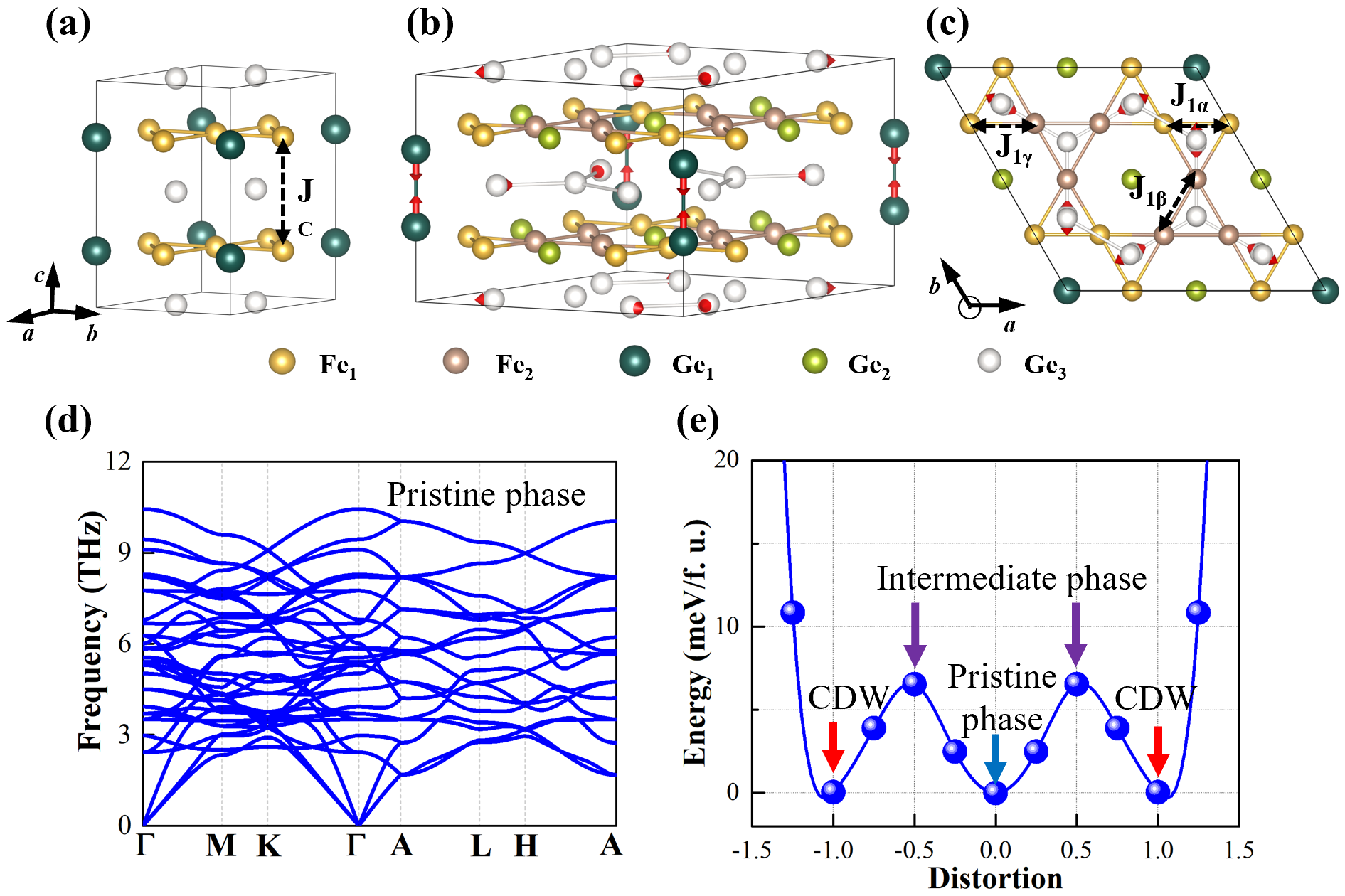
CDW state of FeGe. Traditionally, the CDW phase is generally constructed from the imaginary phonon modes of the pristine phase. This approach, however, is invalid for FeGe as its pristine phase has no imaginary phonon branch as show in Fig.1d. To determine the possible CDW deformation of FeGe, we adopt different supercells and perform DFT calculations on various configurations, generated from the perturbed genetic algorithm[22] (see Methods). Our results show that the 222 CDW state, sharing the same space group of P6/mmm with the pristine phase (Fig.1a), is the most stable among different deformations, consistent with previous studies[12, 21]. As depicted in Figs.1b,c, in the 222 CDW state, there are two inequivalent Fe sites and two inequivalent Ge sites in the kagome layer. The adjacent Ge1 atoms of neighboring layers are strongly dimerized via large displacements (0.65 Å per Ge1) along the c-axis[20], accompanied by minor movements (< 0.08 Å) of other atoms, including the Kekulé distortion in the Ge3 honeycomb atomic layers[12]. As a result, the 222 CDW deformation is mainly characterized by dimerization of Ge1 atoms, distinct from the dominated in-plane displacement of V kagome net found in AV3Sb5[23].
We then look at the energy evolution during the CDW transition. As shown in Fig.1e, both the pristine and CDW phases are located at the energy minima, consistent with their phonon stabilities [see Fig.1d and Fig.S1 in Supplementary Note (SN) 1[24]]. The CDW phase shows a comparable energy ( 0.05 meV/f.u. higher) with respect to the pristine phase and tends to become the energetically favorable one when taking into account the zero-point energy[12] or mildly changing of lattice constants induced by different exchange correlation functionals (see SN 6[24]). The transition from the pristine to CDW phase has to overcome an energy barrier of 6.54 meV/f.u. (that is the energy of the intermediate phase), leading to the peculiar triple-well energy landscape, which is distinct from the double-well scenario in conventional CDW materials.
Mechanism of the CDW transition. To reveal the underlying mechanism of the triple-well picture, we track the DFT band structure evolution during the CDW phase transition as shown in Figs.2d-f (see SN 2 for detailed band structure evolution and SN 3 for unfolded band structure[24]). Since the CDW state of FeGe is dominated by the strong dimerization of Ge1 atoms (Fig.1b), we highlight the bands that consist of Ge1 pz orbitals by blue dots, and mark the bands composed of Ge2 pz orbitals by red dots for comparisons. Interestingly, although the Ge1 and Ge2 bands are degenerate in the undistorted pristine phase, they split into two distinct parts in the CDW phase (Figs.2d,f). Such a splitting can be understood by the schematic plot in Figs.2a,b, where the Ge1 atoms form a triangular sublattice, and the Ge2 atoms form a kagome sublattice. In the CDW phase, the interaction between the two sublattices becomes negligibly weak due to the small overlap of their pz orbitals and large energy difference between Ge1 pz and Ge2 pz orbitals due to the Ge1 dimerization, thereby producing two nearly independent sets of bands. Note that the Ge1 bands presented here all belong to bonding states of the dimerized Ge1 1D chain (the anti-bonding states lie far above the Fermi energy, see SN 7[24]), and therefore exhibit a dramatically downward movement after the strong Ge1 dimerization. By contrast, the Ge2 atoms nearly lie in situ during the CDW transition, leading to almost unshifted bands. To further validate such mechanism, we also construct a TB model for the in-plane Ge atoms (see Methods and SN 9[24]). The calculated TB bands are given in Fig.2b, which well captures the band splitting of the two sublattices.
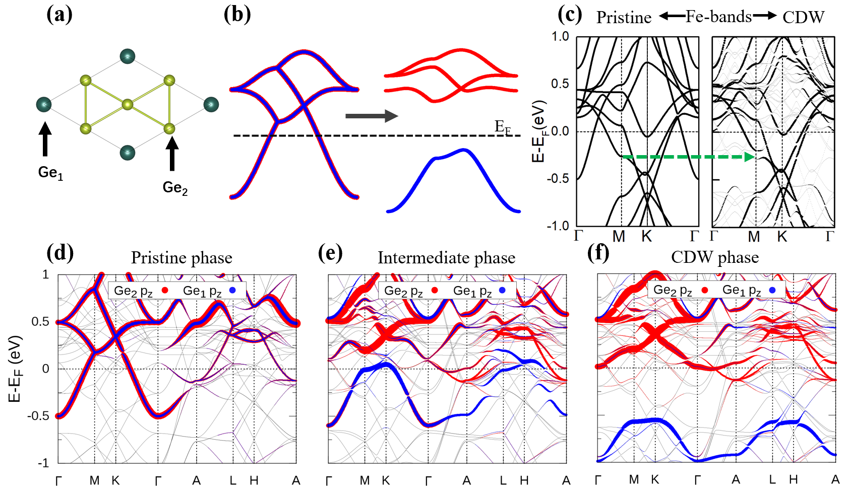
Due to the similarity between the band structure evolutions of spin-up and spin-down channels, we only plot the spin-up channel within a FM layer in the A-AFM state here (see the spin-down channel band structure in SN 2[24]). Note that the plotted Ge-bands in the range of -1 to 1 eV all belong to the bonding states (see SN 7[24]).
We now further understand the triple-well picture by the abovementioned band evolution, in particular the significant downward shift of the Ge1 band during the CDW transition as shown in Figs.2d-f. (i) At the beginning of the distortion, both the M-K and L-H paths of Ge1-band sit well above E. Given that the VHSs of a triangular lattice are located at the M and L points (see SN 4[24]), the downward shift of Ge1-band results in only a slight decrease in the electronic energy since the VHSs remain unoccupied. However, the distortion leads to a considerable increase in the elastic energy, making the pristine phase be stabilized in an energy minimum. (ii) At the intermediate distortion (1/2 distortion in Fig.1e), the flat M-K and L-H paths of Ge1-band begin to be fully occupied as shown in Fig.2e. As a consequence, the downward movement of Ge1 band gives rise to a dramatically decrease in the electronic energy, large enough to overcome the continually increased elastic energy. Accordingly, the total energy starts to drop as shown in Fig.1e. (iii) At fully-developed CDW distortion, the entire Ge1-band has already been fully occupied as shown in Fig.2f. Although its downward shift would continue to decrease the electronic energy, the bond length of Ge1-Ge1 dimer becomes so short that further distortion would leads to a sharp increase in the elastic energy arising from the Pauli repulsion. Consequently, the total energy begins to rise again with increasing the distortion, resulting in an energy minimum for the CDW phase. This process, which can also be clearly seen in the partial density of states (see SN 5[24]), naturally explains the triple-well energy profile of the CDW transition in Fig.1e.
The above band evolution is reminiscent of the well-known Peierls effect[25]. However, this mechanism is distinct from the conventional Peierls effect. Typically, in the Peierls effect the lower band after splitting is always fully occupied, while in our case it is gradually fully filled due to the Fermi energy pinning phenomenon (The Fermi energy varies from 6.05 to 6.00 eV during the CDW transition according to our DFT calculations, which can be regarded as a fixed value). This is because, although the CDW phase takes electrons from the bands near E to fill the Ge1 band, there are plentiful bands contributed by other atoms near E, which act as an electron reservoir that effectively fix the Fermi energy. It is important to note that without the Fermi energy pinning, the energy profile of CDW transition would be a double-well as in the conventional Perierls effect. Hence, we attribute the unique triple-well picture in FeGe to the cooperation between the Peierls-like effect and the Fermi energy pinning phenomenon.
In addition, we also analyze the band structure reconstruction contributed by Fe atoms, and explain why it is unlikely to drive the CDW transition. As shown in Fig.2c, although the CDW phase opens a gap at the VHS (M point as marked by the green dashed arrow), it is located well below the E, resulting in no energy reduction. Moreover, even if supposing the VHS is located near E, the related gap opening would likely to trigger a double-well CDW landscape like that in AV3Sb5, rather than the current triple-well transition. Hence, it is the Ge1 bands instead of the previously proposed Fe bands[11] that drive the triple-well CDW transition in FeGe.
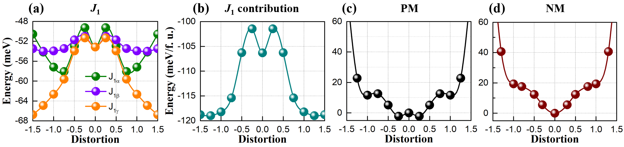
Energy changes related to magnetism. Although we have demonstrated that the CDW phase transition in FeGe is primarily driven by the nonmagnetic (NM) Ge atoms, the role of its A-AFM order, which is generally believed to has a strong interplay with its CDW order[13], is not yet clear. Motivated by this, we calculate the magnetic exchange interactions using the four-state method[26], so as to extract the contribution of magnetism to the CDW transition. For the undistorted phase, the in-plane first-nearest neighbor yields strong ferromagnetism (J1 = -53.16 meV) and dominants over others, while the out-of-plane nearest neighbor favors weak AFM (JC = 8.12 meV) (SN 11[24]). Consequently, it results in the A-AFM ground-state order with the simulated transition temperature being TN 480 K[22], which is close to the experimental value of TN 410 K[16, 17] (see SN 11 for the simulation[24]) and is consistent with previous studies[27]. By comparison, when introducing the CDW structural distortion, the exchange couplings are significantly changed. Here, we take the dominant J1 for example. As the two Fe sites are no longer equivalent in the CDW phase, the J1 splits into J1α, J1β, J1γ, as marked in Fig. 1c. Their values show a sophisticated evolution as a function of the CDW distortion (Fig.3a). Consequently, the J1 contribution (weighted sum of J1α, J1β and J1γ) in Fig.3b displays an approximately triple-well profile, which lower the energy of CDW phase by -10.67 meV/f.u. compared with the pristine phase, indicating the important role of magnetism in the CDW formation. The magnetic interactions between other nearest neighbors are not discussed here due to their negligible contributions (see SN 11 for detail[24]). Based on these calculated magnetic interactions, we also separate the corresponding paramagnetic (PM) contribution from the total energy as depicted in Fig. 3c. The increasing trend from the pristine phase to the CDW phase, that is, the energy cost for structural distortions, provides indirect evidence for the interplay between the CDW and magnetism. Besides, we also plot the energy profile for FeGe in NM state (Fig.3d, see SN 8 for analysis on NM state[24]), which is similar to that of PM state in Fig.3c, again confirming that A-AFM order is crucial for the CDW formation.
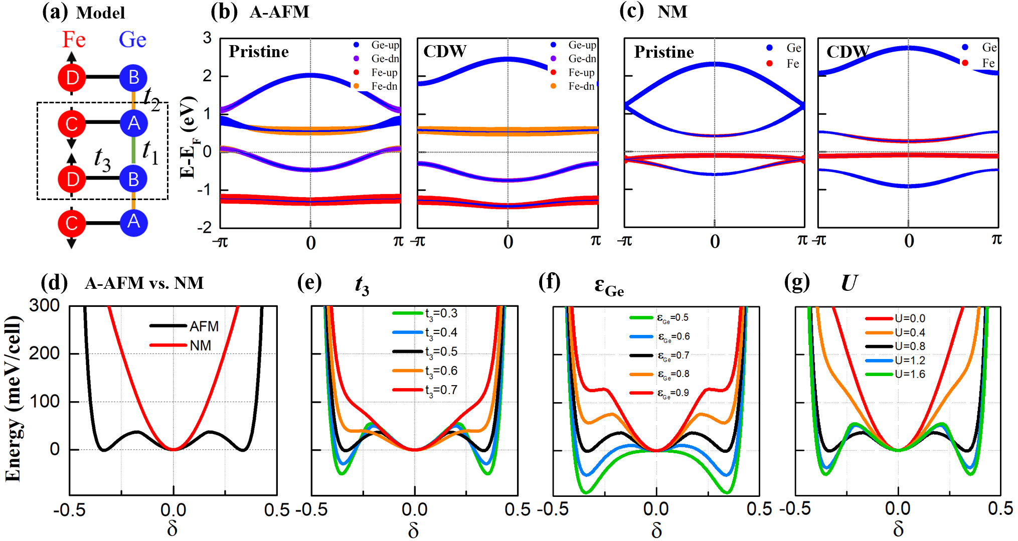
The interplay of magnetism and CDW revealed by tight-binding model. Tight-binding model is developed to get further insights into the interplay of magnetism and CDW transition. As shown in Fig.4a, a simplified one-dimensional atomic structure is adopted with Ge chain being along -axis and each Ge being connected with one Fe. The corresponding Hamiltonian then reads
| (1) |
where
| (2) |
E is the Fermi energy; and are the on-site energy of Ge-pz and Fe-d orbitals with respect to E, respectively; U characterizes the exchange splitting (2U=-, U = 0 for NM case); ti {i = 1, 2, 3} represent the hopping integral between different ions as labeled in Fig. 4a. According to Harrison’s method [28], the dependence of ti on the bond distortion can be written as t1= and t2= (t3 is assumed to be a constant due to the very slightly change of the Fe-Ge bond), where t0 is the hopping integral in the pristine phase, stands for the relative deformation with respect to the pristine undistorted Ge-Ge bond, with = 0.00, 0.16, 0.32 corresponding to the pristine, intermediate and CDW phases in Fig. 1e, respectively.
After diagonalizing the Hamiltonian, the occupation energy of the system can be determined by integrating the eigenvalues below the E. Here, we take into account the aforementioned Fermi energy pinning phenomenon, which arises from the other atoms that are not included in the TB model. Specifically, there exist plentiful bands near the Fermi energy in the DFT electronic structures as shown in Figs.1d-f, which act as a reservoir of electrons that effectively pins the Fermi energy, regardless of the change of occupation number of Ge1 bands during the phase transition. Thus, the almost invariant Fermi energy E, instead of the occupation number, is fixed in our TB model. Considering this, as well as the lattice distortion energy, the total energy can then be expressed as
| (3) |
where the first term is the integrated occupation energy of all eigenvalues with occupations ; the second term gathers the energy contribution from the electrons transfer between the TB bands and the reservoir bands at the E, with N= the integrated number of occupied electrons in the TB bands; the third term represents the lattice distortion energy of Ge-Ge interactions, extracted from the repulsion part of the Lennard–Jones potential[29]; and the last term denotes the Fe-Ge interactions, which is approximated by a simple harmonic form due to the slight change in the Fe-Ge distance from the equilibrium position. By fitting to the DFT electronic structures and total energies (see SN 15[24] for detail), we obtain E = 6.0 eV, = 0.7 eV, = -0.3 eV, U = 0.8 eV, t0 = 0.6 eV, t3 = 0.5 eV, B = 0.001 eV, B2 = 6.8 eV for the A-AFM FeGe. While for the NM FeGe (U = 0 eV), although the absolute values of E+ and E+ remain the same, the E changes to 5.7 eV (see SN 9[24]), which effectively leads to = 1.0 eV, = 0.0 eV, consistent with the Stoner model that the lies near the Fermi energy.
The band structures based on the TB model with the fitted parameters are plotted in Figs. 4b,c. A shift of the entire Ge-band is clearly captured during the CDW phase transition for both A-AFM and NM orders, in line with the DFT calculations (see SN 9[24]). The relative total energy as a function of the distortion is further displayed in Fig.4d, which well confirms the triple-well profile in the A-AFM order and the single-well profile in the NM order. Such distinct energy profiles are mainly associated with the differences in the band structures between the A-AFM and NM states: (i) in the A-AFM state, the Fe-Ge hybridization near E is significantly weaker, since the Fe orbitals are pushed far away from the E by the exchange splitting U; (ii) the location of Ge-band with respect to E (characterized by ) in the pristine state is higher in the NM order than in the A-AFM order, which makes it more difficult for the transition to happen. Such TB results are in line with the DFT calculations (see SN 9[24]).
We now further understand the effect of magnetism on the CDW formation by adjusting the TB parameters independently. We first modify the strength of Fe-Ge hybridization by directly tuning the parameter t3. As shown in Fig.4e, the energy profile evolves from a single-well to a triple-well as t3 decreases. Alternatively, the Fe-Ge hybridization can also be indirectly adjusted via modifying the exchange splitting U. For U = 0 (NM order), the Fe orbitals are close to Ge orbitals near E, giving rise to strong Fe-Ge hybridization. As the value of U increases, the Fe-band is pushed away from E, which weakens the Fe-Ge hybridization, and the energy profile gradually changes from a single-well to a triple-well as shown in Fig.4g. Such results with varying and indicate that a weaker Fe-Ge hybridization is beneficial to form the CDW state with a triple-well potential. Based on finding, we infer that a tensile strain is likely to facilitate the formation of the CDW states due to the weakening of Fe-Ge hybridization under the lattice expansion, which is indeed verified by our further DFT calculations (see SN 6[24]). On the other hand, the initial location of Ge-band () is also responsible for the formation of the CDW state (Fig.4f): (i) for a large , it may cost a high energy to overcome the lattice distortion before the occupation of Ge-bands, causing a single-well energy profile; (ii) for a small (near E), it would lower energy to form the CDW state by the instant splitting of Ge-bands, leading to a double-well energy profile; (iii) for a intermediate , a triple-well profile appears, in line with the aforementioned DFT description. With such further information from TB, the mechanisms is clear for not only the CDW transition of FeGe, but also the fact that the isomorphic FeSn show no experimentally observed CDW phase transition, which probably attributes to the larger “” in the case of FeSn (see SN 10 for details[24]). Given all of the above discussion, it is now clear that the A-AFM order, is critical for forming the triple-well CDW phase transition, since it weakens the Fe-Ge hybridization through the exchange splitting U, and possesses a lower position of Ge-bands with respect to the Fermi energy.
Conclusions
In summary, by applications of DFT and TB model analyses, the mechanism of triple-well CDW in FeGe is revealed as a cooperation between the Peierls-like effect and magnetism. The entire band of Ge1 atom, which hosts a large dimerization, is found to be responsible for the formation of CDW phase. Moreover, it is found that the A-AFM order is critical for lowering energy and stabilizing the CDW phase, through interplay with the structural distortion. We expect the presently discovered new mechanisms not only can be used to understand the CDW transition in FeGe, but also shed light on other systems with intertwined magnetism and CDW.
DFT calculations
DFT calculations are performed using the projector-augmented wave method[30] as implemented in the Viennaab initio Simulation Package (VASP)[31, 32]. The exchange-correlation interactions are described by the generalized-gradient approximation with the Perdew-Burke-Ernzerhof (PBE) functional[33]. An energy cutoff of 350 eV is used for the plane wave basis expansion. All atomic positions are fully relaxed until the force acting on each atom became smaller than eV/Å. To determine the possible CDW deformation of FeGe, we adopt the genetic algorithm for structure research, as implemented in the PASP software[22]. In the 112 pristine phases, the calculated lattice constants are 4.97 Å(a = b) and 8.11 Å(c). The Brillouin zone is sampled with a 161610 k-point mesh in the 112 primitive cell. A 8810 mesh is used for the 222 supercell. k-meshes of 282818 and 161618 are used to calculate the band structures of the pristine and 222 CDW phases, respectively. To visualize the effect of structural deformation to the electronic structure, the effective band structure of CDW states is unfolded to the pristine Brillouin zone by the band-unfolding method using vaspkit code[34]. The phonon dispersion is calculated by using the finite displacement method as implemented in the phonopy code[35]. In calculating the phonon spectrum, a 996 mesh is used for 222 supercell of the pristine phase, and 8810 mesh for 111 supercell of the CDW phases. The four-state energy mapping method[26] was performed to obtain magnetic parameters from DFT total energies, for which the 1 CDW supercell and 4410 mesh were adopted. In calculating single-ion anisotropy, the spin-orbit coupling was included. Monte Carlo (MC) simulations were performed using the calculated magnetic exchange interactions. The 30301 supercells were adopted in the study. For each configuration, 10000 and 100000 MC steps per site were performed for equilibrating the system and statistical averaging, respectively.
TB models
In the one-dimensional atomic chain model, the single electron Schrödinger equation can be repressed as
| (4) |
where the wave function and Hamiltonian can be written as
| (5) |
| (6) |
where cu is the weights of the linear combination, L is the lattice vector, u describes the real space translation vector of u-atom in the unit cell (see Fig.4a, here, u=1,2,3,4, denoting GeA, GeB, FeC, FeD, respectively). Hvu() from Eq.6 are the matrix elements of the Hamiltonian, which can be further expressed using the on-site energy i {i = Ge, Fe} and hopping terms ti {i = 1, 2, 3} (see Fig.4a). Then the tight-binding Hamiltonian is given as Eq.2.
Likewise, the Hamiltonian for the spinless Ge atoms in two-dimensional lattice can be expressed as
| (7) |
where i is the on-site energy of atom i (in the 2×2 cell, there are four Ge atoms, denoting 1, 2, 3, 4, respectively, see Fig.S15[24]). tij is the hopping term between i and j, belonging to different sublattices. Corresponding Hamiltonian H can be expressed as
| (8) |
Here, ij represent the possible combination vectors between i and j, which can contain both the nearest-neighbor and next nearest-neighbor interactions. After solving the Hamiltonian matrix, we can have: (i) for the undistorted pristine phase, all four Ge atoms are equivalent, 1 = 2, t12 = t34, corresponding to the degenerate energy eigenvalues as plotted in Fig.2b (left side); (ii) when the CDW distortion occurs, the initial equivalent Ge atoms split into one triangular band consisting of Ge1 atom and three kagome bands consisting of Ge2 atoms (right side in Fig.2b), revealing good agreement with DFT calculations.
All the data supporting the findings of this study are provided within this paper and its Supplementary Information files. All the raw data generated in this study are available from the corresponding author upon reasonable request.
We thank Prof. Guoqing Chang for useful discussions. We acknowledge financial support from the Ministry of Science and Technology of the People’s Republic of China (No. 2022YFA1402901), the support from NSFC (grants No. 11825403, 11991061, 12188101, 12174060, and 12274082), and the Guangdong Major Project of the Basic and Applied Basic Research (Future functional materials under extreme conditions–2021B0301030005). C. X. also acknowledge the support from Shanghai Science and Technology Committee (grant No. 23ZR1406600). B. Z. also acknowledge the support from China Postdoctoral Science Foundation (grant No. 2022M720816).
Correspondence should be addressed to C.X. (csxu@fudan.edu.cn) and H.X. (hxiang@fudan.edu.cn).
References
References
- [1] G. Grüner, “The dynamics of charge-density waves,” Reviews of modern physics, vol. 60, no. 4, p. 1129, 1988.
- [2] C. Varma and A. Simons, “Strong-coupling theory of charge-density-wave transitions,” Physical review letters, vol. 51, no. 2, p. 138, 1983.
- [3] M. Johannes and I. Mazin, “Fermi surface nesting and the origin of charge density waves in metals,” Physical Review B, vol. 77, no. 16, p. 165135, 2008.
- [4] S. Zybtsev, V. Y. Pokrovskii, and S. Zaitsev-Zotov, “’quantized’states of the charge-density wave in microcrystals of K0.3MoO3,” Nature communications, vol. 1, no. 1, p. 85, 2010.
- [5] S. V. Zaitsev-Zotov, “Finite-size effects in quasi-one-dimensional conductors with a charge-density wave,” Physics-Uspekhi, vol. 47, no. 6, p. 533, 2004.
- [6] Z. Wang and S.-C. Zhang, “Chiral anomaly, charge density waves, and axion strings from weyl semimetals,” Physical Review B, vol. 87, no. 16, p. 161107, 2013.
- [7] B. R. Ortiz, L. C. Gomes, J. R. Morey, M. Winiarski, M. Bordelon, J. S. Mangum, I. W. H. Oswald, J. A. Rodriguez-Rivera, J. R. Neilson, S. D. Wilson, E. Ertekin, T. M. McQueen, and E. S. Toberer, “New kagome prototype materials: Discovery of KV3Sb5, RbV3Sb5, and CsV3Sb5,” Phys. Rev. Mater., vol. 3, no. 9, p. 094407, 2019.
- [8] B. R. Ortiz, S. M. L. Teicher, Y. Hu, J. L. Zuo, P. M. Sarte, E. C. Schueller, A. M. M. Abeykoon, M. J. Krogstad, S. Rosenkranz, R. Osborn, R. Seshadre, L. Balents, J. He, and S. D. Wilson, “CsV3Sb5: A Z2 topological kagome metal with a superconducting ground state,” Phys. Rev. Lett., vol. 125, no. 24, p. 247002, 2020.
- [9] B. R. Ortiz, P. M. Sarte, E. M. Kenney, M. J. Graf, S. M. Teicher, R. Seshadri, and S. D. Wilson, “Superconductivity in the Z2 kagome metal KV3Sb5,” Physical Review Materials, vol. 5, no. 3, p. 034801, 2021.
- [10] H. Miao, T. Zhang, H. Li, G. Fabbris, A. Said, R. Tartaglia, T. Yilmaz, E. Vescovo, J. Yin, S. Murakami et al., “Spin-phonon coupling driven charge density wave in a kagome magnet,” arXiv preprint arXiv:2210.06359, 2022.
- [11] X. Teng, J. S. Oh, H. Tan, L. Chen, J. Huang, B. Gao, J.-X. Yin, J.-H. Chu, M. Hashimoto, D. Lu et al., “Magnetism and charge density wave order in kagome FeGe,” Nature Physics, pp. 1–9, 2023.
- [12] S. Shao, J.-X. Yin, I. Belopolski, J.-Y. You, T. Hou, H. Chen, Y. Jiang, M. S. Hossain, M. Yahyavi, C.-H. Hsu et al., “Intertwining of magnetism and charge ordering in kagome FeGe,” ACS nano, 2023.
- [13] X. Teng, L. Chen, F. Ye, E. Rosenberg, Z. Liu, J.-X. Yin, Y.-X. Jiang, J. S. Oh, M. Z. Hasan, K. J. Neubauer et al., “Discovery of charge density wave in a kagome lattice antiferromagnet,” Nature, vol. 609, no. 7927, pp. 490–495, 2022.
- [14] J.-X. Yin, Y.-X. Jiang, X. Teng, M. S. Hossain, S. Mardanya, T.-R. Chang, Z. Ye, G. Xu, M. M. Denner, T. Neupert et al., “Discovery of charge order and corresponding edge state in kagome magnet FeGe,” Physical Review Letters, vol. 129, no. 16, p. 166401, 2022.
- [15] T. Ohoyama, K. Kanematsu et al., “A new intermetallic compound FeGe,” Journal of the Physical Society of Japan, vol. 18, no. 4, pp. 589–589, 1963.
- [16] J. Bernhard, B. Lebech, and O. Beckman, “Neutron diffraction studies of the low-temperature magnetic structure of hexagonal FeGe,” Journal of Physics F: Metal Physics, vol. 14, no. 10, p. 2379, 1984.
- [17] J. Bernhard, B. Lebech, and O. Beckman, “Magnetic phase diagram of hexagonal FeGe determined by neutron diffraction,” Journal of Physics F: Metal Physics, vol. 18, no. 3, p. 539, 1988.
- [18] L. Wu, Y. Hu, D. Wang, and X. Wan, “Novel three-dimensional fermi surface and electron-correlation-induced charge density wave in FeGe,” arXiv preprint arXiv:2302.03622, 2023.
- [19] Z. Zhao, T. Li, P. Li, X. Wu, J. Yao, Z. Chen, S. Cui, Z. Sun, Y. Yang, Z. Jiang et al., “Photoemission evidence of a novel charge order in kagome metal fege,” arXiv preprint arXiv:2308.08336, 2023.
- [20] Y. Wang, “Enhanced spin-polarization via partial Ge1-dimerization as the driving force of the 2222 CDW in FeGe,” arXiv preprint arXiv:2304.01604, 2023.
- [21] Z. Chen, X. Wu, S. Zhou, J. Zhang, R. Yin, Y. Li, M. Li, J. Gong, M. He, Y. Chai et al., “Long-ranged charge order conspired by magnetism and lattice in an antiferromagnetic kagome metal,” arXiv preprint arXiv:2307.07990, 2023.
- [22] F. Lou, X. Li, J. Ji, H. Yu, J. Feng, X. Gong, and H. Xiang, “PASP: Property analysis and simulation package for materials,” J. Chem. Phys., vol. 154, no. 11, p. 114103, 2021.
- [23] H. Tan, Y. Liu, Z. Wang, and B. Yan, “Charge density waves and electronic properties of superconducting kagome metals,” Phys. Rev. Lett., vol. 127, no. 4, p. 046401, 2021.
- [24] See Supplemental Material at http://link for more information.
- [25] M. Fowler, “Electrons in one dimension: the peierls transition,” Introduction: Looking for Superconductors and Finding Insulators, p. 20, 2007.
- [26] H. Xiang, C. Lee, H.-J. Koo, X. Gong, and M.-H. Whangbo, “Magnetic properties and energy-mapping analysis,” Dalton Transactions, vol. 42, no. 4, pp. 823–853, 2013.
- [27] H. Zhou, S. Yan, D. Fan, D. Wang, and X. Wan, “Magnetic interactions and possible structural distortion in kagome FeGe from first-principles study and symmetry analysis,” arXiv preprint arXiv:2211.15545, 2022.
- [28] W. A. Harrison, Elementary electronic structure (revised edition). World Scientific Publishing Company, 2004.
- [29] H. Wei, Y. Yang, S. Chen, and H. Xiang, “Lead-free hybrid perovskite N(CH3)4SnI3 with robust ferroelectricity induced by large and non-polar N(CH3)4+ molecular cation,” Nature Communications, vol. 12, no. 1, p. 637, 2021.
- [30] P. E. Blöchl, “Projector augmented-wave method,” Phys. Rev. B, vol. 50, no. 24, p. 17953, 1994.
- [31] G. Kresse and J. Furthmüller, “Efficiency of ab-initio total energy calculations for metals and semiconductors using a plane-wave basis set,” Comput. Mater. Sci., vol. 6, no. 1, pp. 15–50, 1996.
- [32] G. Kresse and J. Furthmüller, “Efficient iterative schemes for ab initio total-energy calculations using a plane-wave basis set,” Phys. Rev. B, vol. 54, no. 16, p. 11169, 1996.
- [33] J. P. Perdew, K. Burke, and M. Ernzerhof, “Generalized gradient approximation made simple,” Phys. Rev. Lett., vol. 77, no. 18, p. 3865, 1996.
- [34] V. Wang, N. Xu, J.-C. Liu, G. Tang, and W.-T. Geng, “VASPKIT: A user-friendly interface facilitating high-throughput computing and analysis using VASP code,” Comput. Phys. Commun., vol. 267, p. 108033, 2021.
- [35] A. Togo and I. Tanaka, “First principles phonon calculations in materials science,” Scr. Mater., vol. 108, pp. 1–5, 2015.