TRonly\BODY \NewEnvironJonly
The ExaNeSt Prototype:
Evaluation of Efficient HPC Communication Hardware
in an ARM-based Multi-FPGA Rack
Abstract.
ABSTRACT:
We present and evaluate the ExaNeSt Prototype, a liquid-cooled rack prototype consisting of 256 Xilinx ZU9EG MPSoCs, 4 TBytes of DRAM, 16 TBytes of SSD, and configurable interconnection 10-Gbps hardware. We developed this testbed in 2016-2019 to validate the flexibility of FPGAs for experimenting with efficient hardware support for HPC communication among tens of thousands of processors and accelerators in the quest towards Exascale systems and beyond. We present our key design choices reagrding overall system architecture, PCBs and runtime software, and summarize insights resulting from measurement and analysis.
Of particular note, our custom interconnect includes a low-cost low-latency network interface, offering user-level zero-copy RDMA, which we have tightly coupled with the ARMv8 processors in the MPSoCs. We have developed a system software runtime on top of these features, and have been able to run MPI. We have evaluated our testbed through MPI microbenchmarks, mini, and full MPI applications. Single hop, one way latency is s; approximately s out of these are attributed to network interface and the user-space library that exposes its functionality to the runtime. Latency over longer paths increases as expected, reaching s for a five-hop path. Bandwidth tests show that, for a single hop, link utilization reaches of the theoretical capacity. Microbenchmarks based on MPI collectives reveal that broadcast latency scales as expected when the number of participating ranks increases. We also implemented a custom Allreduce accelerator in the network interface, which reduces the latency of such collectives by up to . We assess performance scaling through weak and strong scaling tests for HPCG, LAMMPS, and the miniFE mini application; for all these tests, parallelization efficiency is at least , or better.
1. Introduction
High Performance Computation (HPC) is a key necessity in numerous domains of modern society, such as weather forecast and the environment, molecular dynamics, chemistry, biology and medicine, fluid dynamics, engineering and industrial design, astronomy and physics, data analytics, economy and sociology, and so on. All of these heavily depend on the processing capabilities offered by parallel machines. The increasing demand for both processing and storage leads to the growth of HPC machines in both size and complexity, resulting in problems of scalability. To overcome these challenges, the development of novel interconnect technologies for building efficient and scalable HPC systems is essential. The design and tuning of interconnects for many thousands of nodes, the network interfaces, software drivers, operating system (OS) libraries and runtime systems are all crucial for the success of HPC machines.
In modern HPC systems, the complexity of the machine increases sharply, requiring Graphics Processing Units (GPUs) or Field-Programmable Gate Arrays (FPGAs) to accelerate critical computation and communication tasks, thus offloading the Central Processing Units (CPUs). The memory hierarchy also deepens, driving the need for high network bandwidth and efficient interfaces. Managing the complexity of such systems while delivering high performance requires tuned and efficient runtimes. Additionally, energy consumption is a major challenge in large and extreme scale systems(6012897, ). Hence, a parallel approach, based on low-power ARM processors and reconfigurable logic, has demonstrated promising results(9041710, ). Finally, low-power FPGAs are emerging as potential competitors to accelerators such as GPUs and Vector processors for a wide range of applications (Blott16, ; Cilardo18, ; 10.1145/3149457.3149479, ; Escobar16, ).
In this paper, we present and evaluate the multi-FPGA ExaNeSt prototype, which we designed and built as an experimentation vehicle for the development of complex large-scale systems. The platform is a result of 4 years of collaboration (7723536, ) between academic institutes and industrial partners in Europe under the European Exascale System Interconnect and Storage (ExaNeSt) EU project (exanesturl, ). This effort was motivated by the trend towards HPC systems built using micro-servers (Oleksiak2019, ; montblanc2020, ) or processors commonly used in embedded SoCs (1592896, ), so as to reduce power consumption. The design of the ExaNeSt compute node, the Quad FPGA Daughter Board (QFDB)(qfdb_paper, ), was based on tightly-coupled low-power ARM-based Multi-Processor Systems-on-Chip (MPSoCs) and liquid cooling (trets20, ), to improve compute density and reduce energy consumption.
The ExaNeSt prototype rack consists of 48 QFDB modules (each containing 4 FPGAs), hosted in 12 blades, thus aggregating 192 FPGA MPSoCs. It is split into two sub-systems, with the larger of them consisting of 8 blades. The topology implemented is a three-dimensional (3D) torus. While the ExaNeSt prototype is not an actual HPC machine, we use it to emulate and evaluate HPC systems and their custom interconnect technologies. The reconfigurable nature of FPGAs allows for efficient customization of the communication infrastructure, which is a crucial factor for overall system performance.
We leveraged the ExaNeSt platform to develop a low-cost, high-performance, low-latency interconnect, ExaNet, suitable for both application (HPC) and storage traffic. ExaNet consists of Network Interfaces (NIs), developed within this Lab, and Routers, derived from APENET (ammendola2004apenet, ) and developed in INFN, Italy.
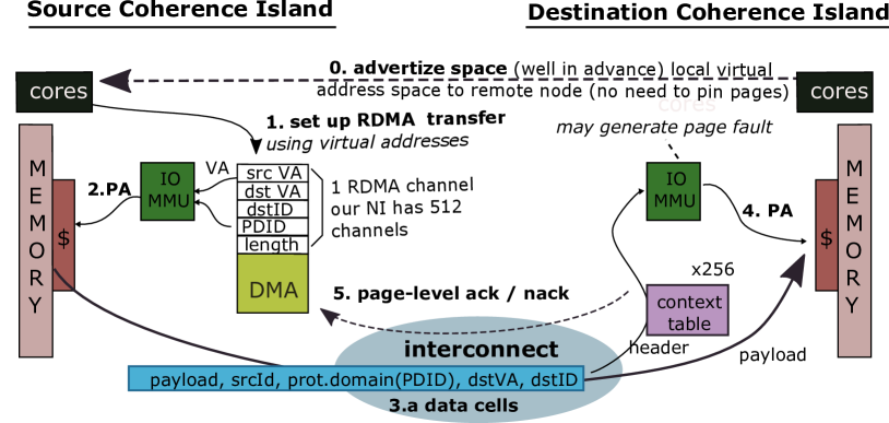
The ExaNet NIs are simple, efficient, and integrated inside the same FPGA chips as the ARMv8 processors, in every node of the system (in each of the 4 FPGAs in every QFDB). In our implementation, the NI occupies less than 10% of the Zynq Ultrascape+ Xilinx FPGA (ZynqTRM, ). It was co-designed together with the software MPI runtime, with simplicity and high performance in mind. Integration of the NI in the same chip with the processors offers advantages: (i) it obviates the need for bulky and costly Network Interface Cards (NICs) connected over PCI; and (ii) tight integration reduces message latency. Despite its low-cost, the ExaNet NI supports user-level, protected, zero-copy Remote Direct Memory Access (RDMA) that bypasses the OS kernel, in order to achieve low latency and low CPU overhead. It leverages the Input/Output Memory Management Unit (IOMMU) that accompanies the ARM processors to translate user-level Virtual Addresses into Physical Addresses, thus avoiding the need for virtual-physical-pair page registrations in the NIC. Effectively, payload destination addresses (80 bits) route packets across the protected Global Virtual Address Space offered by the testbed.
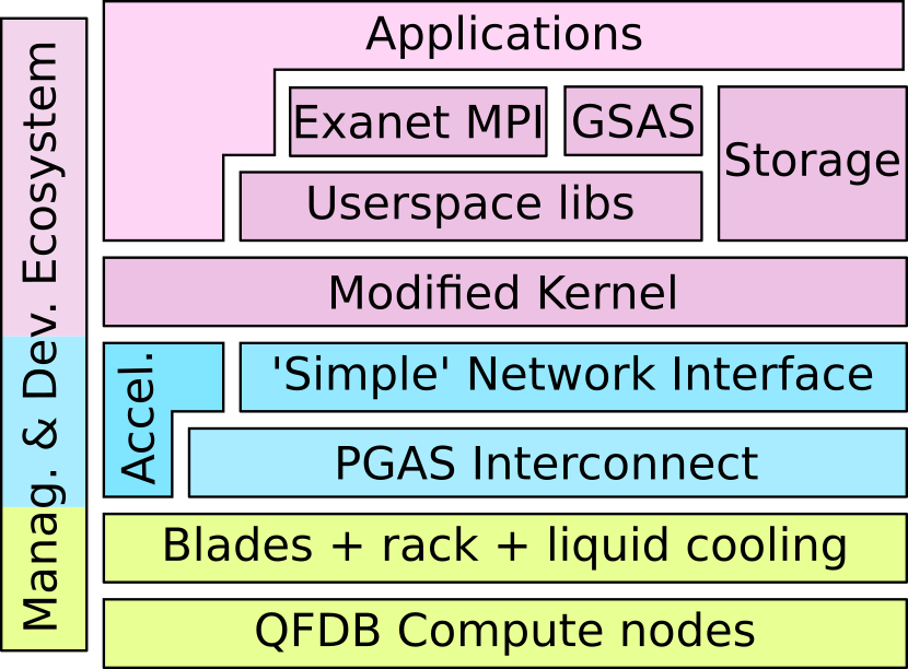
The ExaNet NI offers 1024 RDMA hardware channels to user processes for high-throughput reliable transfers between local and remote virtual addresses. These RDMA channels implement an one-to-one transport for large transfers. The NI further provides channels suitable for many-to-one communication of short messages at low latency (packetizer-mailbox). In order to utilize these channels, key tweaks were made to the Linux kernel and drivers, and user space libraries have been implemented. On top of that, we have implemented an efficient partial implementation of the MPI standard in a Global Shared Address Space (GSAS) environment. This implementation offers the most commonly used point-to-point and collective primitives. Figure 1 presents a high level, bottom up view of the full system derived, including main hardware components, FPGA functionality and the corresponding software ecosystem.
We evaluated the proposed ExaNeSt communication infrastructure using MPI micro-benchmarks, a miniAPP, and two full MPI applications. The point-to-point based microbenchmark showed a one-way single hop latency of s with a hardware-related contribution of approximately s. The achieved throughput over a single link reached of the theoretical capacity for large message sizes. A simple model for broadcast latency showed that the observed latency scaled as expected. Most notable deviations correspond to small messages and can be at most . Note though that, for small messages, actual transfer times are quite small and are thus, more susceptible to system noise.
The performance of the proposed interconnect and software stack was assessed through a mini application (miniFE) and two full MPI applications (HPCG and LAMMPS), with weak and strong scaling tests for all applications, and with a varying number of processes –from one process up to full prototype capacity (i.e. processes). Results showed that efficiency was at least for all HPCG and LAMMPS tests, and for the miniFE’s weak scaling test with 512 processes, where the highest percentage of communication time was observed. Overall, the latency and bandwidth results are quite promising for the efficiency of the network interface, and there is potential for even better performance if the NI gets integrated in ASIC form together with the processor cores. The tests performed on the prototype revealed quite promising scaling properties across the available range of process counts.
We consider the following to be the main contributions of the ExaNest prototype:
-
•
Multi-processor testbed with configurable hardware support for communication - The first platform to integrate 256 FPGAs and offering a multi-processor environment with configurable communication
-
•
Dense node-level and system-level integration - At the node level, the ExaNest prototype integrates 4 FPGAs (ZU9EG MPSoCs), 4 DRAM modules (DDR4 SODIMMs), and an M.2 Solid-State Disk (SSD) on a 120mm x 130mm x 21mm compute node. At the system level, the ExaNest prototype integrates four such compute nodes into a liquid-cooled thin (47mm thickness) blade for optimal thermal management and high-density computing
-
•
Low-cost, low-latency Network Interface offering virtualization and fast completion notifications, tightly coupled with the ARMv8 processing cores
-
•
A custom MPI runtime leveraging Network Interface’s capabilities for user-level zero-copy transfers
The remaining paper is structured as follows. In Section 2, the state of the art is presented and our contributions are placed in that context. In Section 3, the components of the ExaNeSt platform are described: they provide a unrivaled level of flexibility for experimenting with software and firmware configurations. In Section 4, the hardware elements of the ExaNeSt-based interconnect are discussed; and Section 5 details the various software layers that leverage the interconnect. Section 6 presents experimental results that highlight the merits of the ExaNeSt fabric, and Section 7 illustrates the use of hardware accelerators in the ExaNeSt platform. Finally, Section 8 concludes the paper.
2. Related Work
Compared to currently available platforms, ExaNeSt mainly focuses on providing a flexible inter-processor network connectivity in a large-scale system. To the best of our knowledge, ExaNeSt is the first prototype employing up to 128 tightly coupled ZU9EG MPSoCs, each one integrating an ARM Cortex-A53 quad-core processor and an FPGA in the same chip package. The ExaNest architecture gives us the opportunity to emulate and test the efficiency and scalability of different network interfaces and topologies. The ZU9EG FPGA can emulate any network interface directly attached to the ARM processor, since the communication path between the processor and the FPGA includes only a high-performance AXI interconnect instead of a more complex PCIe interface. Moreover, tens of 10 Gb/s inter-MPSoC links are utilized to set up different network topologies.
Although there is significant research on FPGA-based multi-node systems (Escobar16, ), so far there are not many large FPGA-based infrastructures. Some example multi-FPGA platforms are the following: the multi-FPGA MareNostrum Experimental Exascale Platform (meep, ) designed to explore future RISC-V supercomputers, the Novo-G# system (7761639, ), which integrates 448 Stratix FPGAs, the Rivyera cluster from SciEngines employing up to 128 Xilinx Spartan FPGAs per machine (rivyera, ), the 64-FPGA Maxwell supercomputer at the University of Edinburgh (maxwell, ), the 512-FPGA Cube cluster at the Imperial College (cube, ), and lately the AMD HACC clusters (amd-hacc, ), among which the Paderborn University cluster hosts 48 Xilinx Alveo U280 and 32 BittWare 520N FPGA boards. Moreover, there are commercial multi-FPGA platforms such the Maxeler MPC nodes (maxelerMPC-web, ), which accelerate applications on reconfigurable Data Flow Engines (DFEs) (maxelerDFE, ; maxelerDFE-SIGARCH, ; maxelerDFE-web, ), the Amazon EC2 F1 instances containing up to eight FPGAs (amazon-ec2-f1, ), and the Convey HC-2 system (Convey, ), which incorporates a hybrid-core computer that tightly integrate two industry standard Intel Xeon processors with four Xilinx Virtex FPGAs, along with a very powerful memory subsystem.
Several of these systems employ commercial FPGA boards, such as the Xilinx Alveo accelerator cards (alveo-web, ), the Bittware FPGA accelerator boards (bittware-web, ), the Hitech Global development boards (hitechglobal-web, ) or the Digilent boards (digilent-web, ). These systems use mainly PCIe in order to transfer data between the host processors and the FPGA boards, while the inter-node communication is usually based on standard Ethernet or InfiniBand, limiting flexibility for testing new network interfaces and infrastructures.
The FPGAs in these multi-FPGA systems are mainly used as acceleration engines. Indeed, there exist several commercial parallel systems demonstrating that FPGAs constitute an energy efficient and flexible choice for several parallel applications. Microsoft uses FPGAs in its Bing search engine (catapultACM, ; catapultISCA, ) under the Catapult project to achieve 95% higher performance at the cost of 10% higher power consumption. Cray delivers a CS500 cluster system with Stratix FPGAs for the Noctua project (Plessl18, ). Baidu is using low-cost FPGAs to accelerate Deep Neural Networks (Ouyang14, ), while IBM deploys FPGAs for large NoSQL data stores (noSQL, ).
Using the ExaNeSt configurable network infrastructure, we developed the ExaNet interconnect, which was evaluated on 128 ZU9EG to better understand the scalability and the effectiveness of the proposed solution. ExaNet is a low-latency HPC interconnect based on a Partitionned Global Address Space (PGAS) and lean Network Interfaces. For medium and large-scale systems, the user traffic between processors, such as MPI communication between nodes and I/O, usually transits over a low-latency, high throughput network (e.g. Mellanox InfiniBand, Cray Aries, Intel Omni-Path Architecture (OPA)). InfiniBand is the most widely used network in large supercomputers, such as the Summit supercomputer (summitNetwork, ). The latest commercially available InfiniBand products are based on the NDR (Next Data Rate) standard, supporting up to 400 Gb/s per port. In 2015, Intel introduced Omnipath, an HPC interconnect running at 100 Gb/s per port. It was available both as standalone PCIe adapters but also integrated into certain Skylake and Knights Landing CPUs, as an extra chip. Lately, ATOS introduced the Bull eXascale Interconnect (BXI) (bxi, ), which is integrated in the Atos BullSequana XH (sequana-web, ).
Compared to the aforementioned Network Interfaces, ExaNet provides a customizable solution which offers low latency, scalability and coherent communication. In this work, we propose simple but generic network interface primitives that can be integrated in the same chip with the main processor. In order to achieve low latency and low CPU overhead, the network interface supports virtualized, user-level initiated, protected and reliable bulk transfers that completely bypass the kernel. Integrating the Network Interface in the same chip (or package) with the processors and the memory interconnect offers the possibility to use the same block both for on-chip and system level communication, thus saving cost and reducing the silicon area footprint. In our scheme, the network interface exploits the IOMMU, which is close to the processor, in order to translate process-level virtual addresses to physical memory pages, thus avoiding the need for a separate, synchronized translation mechanism inside the network interface card. Moreover, we do not need to pin the pages involved in the communication (psistakis2020part, ), since we handle the occasional page faults that may occur in RDMA transfers by retransmitting the failing packets in hardware.
We have further evolved this Network Interface architecture with congestion management capabilities (congestion18, ) and we have further improved its functionality by offloading more tasks in hardware, without significantly impacting the small footprint of the design.
3. The ExaNeSt platform
The design of an entire High Performance Computing system is extremely demanding, due to the variety of the required skills and the scores of pitfalls that take shape during the development process. In this Section, we present important components of the ExaNeSt platform, ranging from compute hardware to system and management software, with a focus on the caveats that we faced and the techniques that we employed to address them. Overall, the design process was driven by the following goals:
-
•
Low power and high node density targeting HPC demands
-
•
High flexibility for both software and hardware infrastructures
-
•
Lean high-speed interconnection network
3.1. The ExaNeSt compute node: Quad-FPGA Daughter Board
In order to enable the development of custom hardware architectures, the ExaNeSt compute node includes Field Programmable Gate Arrays (FPGAs). We selected the Xilinx Zynq Ultrascale+ device, which, at that time, was the state-of-the-art device, providing both a large Programmable Logic Array and a tightly coupled multi-core ARM processor in the same package. Furthermore, many aspects of the board design were driven by our density goals, and, to date, the ExaNeSt compute node is denser than any other FPGA-based daughter board publicly available. Each compute node, named Quad-FPGA Daughter Board (QFDB), hosts 4 Xilinx ZU9EG MPSoCs. A top-level diagram of the QFDB is presented in Figure 2. In addition to the four FPGAs connected to each other directly, each QFDB supports a large amount of memory and an SSD storage, all within a small footprint (120 mm 130 mm). The top right MPSoC in Figure 2, referred to as the “Network MPSoC”, is responsible for cross-QFDB connectivity.
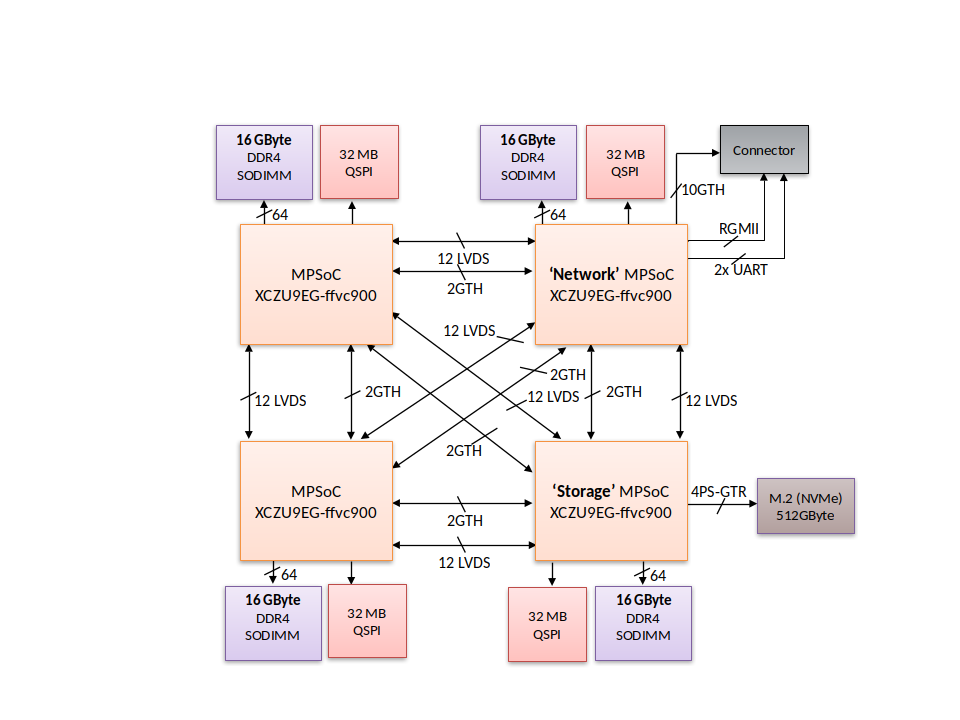
Each MPSoC integrates a quad-core ARM Cortex-A53 processor, with CPU frequency at up to 1.3 GHz, numerous peripherals, and reconfigurable logic. A 16-GByte DDR4 memory module is connected to the ARM processor of each MPSoC. 16 LVDS pairs and 2 high-speed Xilinx GTH transceivers between each pair of MPSoCs provide a low-latency communication channel and a high-bandwidth communication channel, respectively. The LVDS pairs offer a total bandwidth of up to 12.8 Gb/s in each direction between each MPSoC pair, while two GTH links offer a total bandwidth of up to 32 Gb/s, as each GTH transceiver can reach up to 16 Gb/s. The ”Network MPSoC” provides connectivity to the external world through 10 GTH high-speed links. Section 4.1 further describes the topology implemented using those high-speed links. The bottom right FPGA, referred to as the “Storage MPSoC”, provides connectivity to the NVMe storage through the Xilinx PS-GTR transceivers implementing a 4xPCIe Gen 2.0 channel.
The PCB supports hundreds of high-speed signals (96 LVDS pairs, four 72-bit SODIMMS, 22 16 Gb/s high-speed links, etc.) and thus the routing of the high-speed signals, including the DDR and the high-speed serial signals, was very challenging. Short traces for the high-speed signals were possible with the appropriate component placement. The PCB stack-up includes 16 layers: 3 layers for routing the high-speed signals, 3 layers for routing the low-speed signals and 10 layers for ground and voltages. The PCB layout is hierarchical, with the bottom level including a module which contains one MPSoC, its DDR memory, regulators, sensors and clock generators. The top level layout design includes 4 interconnected bottom-level modules and the rest of the components, such as the connectors, additional regulators and sensors.
The board uses a 48V power input, while a series of voltage regulators provide the appropriate voltages to various components of the board. Cyntec and Texas Instruments regulators were used since they offered high efficiency (about 95%) and compact solutions. Twelve power sensors were placed at the output of the high-power regulators. Overall, each QFDB consumes between 20 Watts when idle and 200 Watts, for the most demanding hardware accelerators.
Due to the board density, bring-up activities required substantial time and effort, in large part because of the board density, which impeded many measurements and workarounds at the PCB-level. In order to mitigate those limitations, we leveraged the flexibility of the FPGAs to experiment and monitor the board. Finally, since our HPC testbed consists of dozens of QFDBs, we faced manufacturing concerns, and in turn we built a semi-automated test procedure to validate each QFDB upon procurement or during maintenance phases.
3.2. High-density Liquid-cooled ExaNeSt cabin
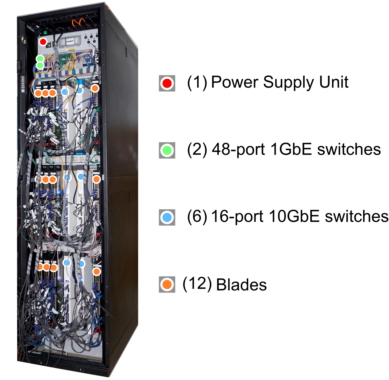
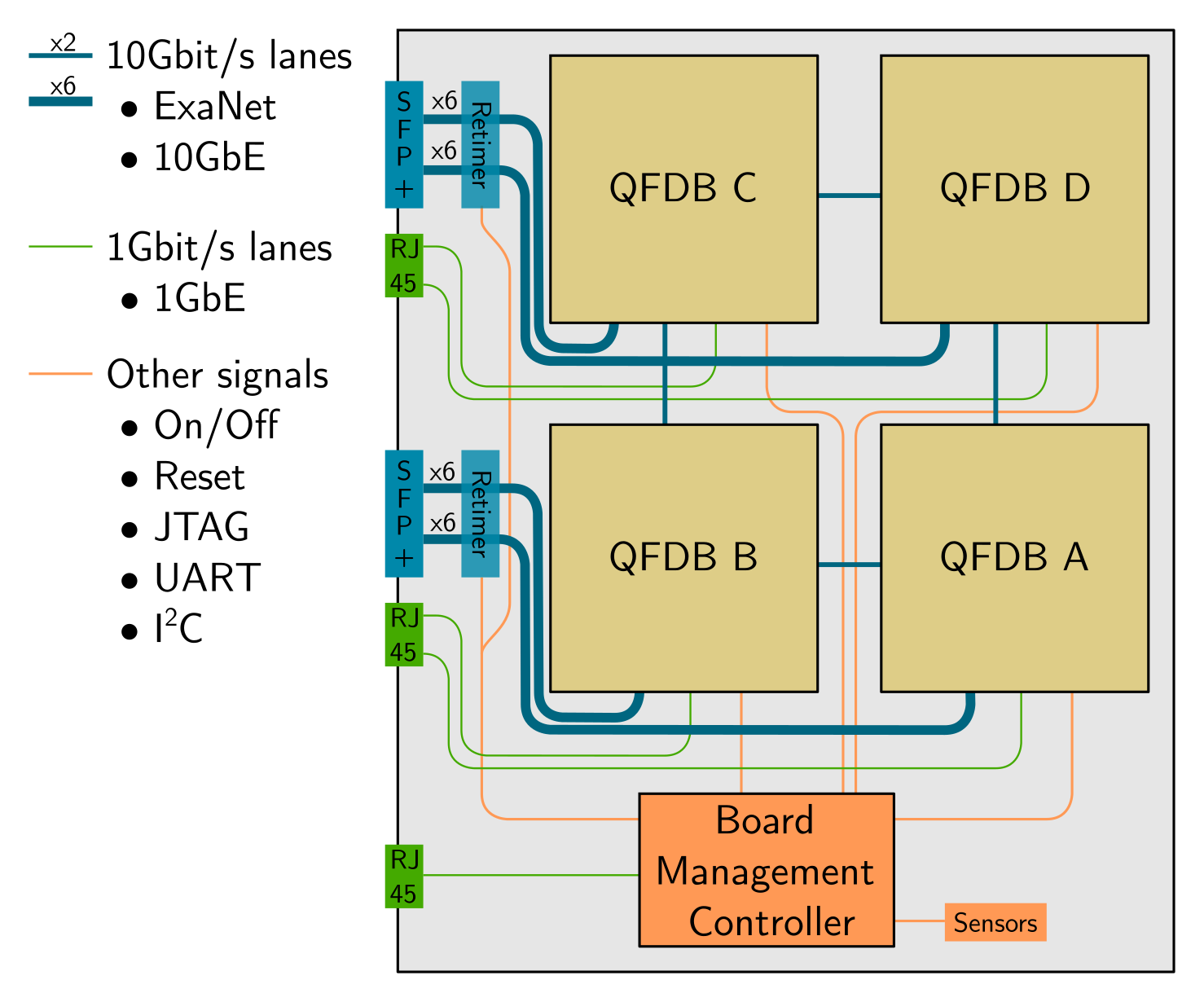
In order to improve the compute and power density, a liquid-cooled cabin was designed to host the system, as shown in Figure 3. The mechanical chassis, power supply and liquid cooling system were provided by ICEOTOPE (iceotope, ). In order to densely host compute nodes, ICEOTOPE also developed a custom liquid-cooled blade to interconnect and manage multiple QFDBs. Figure 4 gives an overview of this board. Each blade hosts 4 QFDBs and a Board Management Controller (BMC), and offers power delivery and highly efficient cooling. The BMC is responsible for managing and controlling the QFDBs (e.g. power cycling, accessing serial ports and JTAG programming) as well as for configuring the blade. In addition, the blade provides high-speed connectivity among the QFDBs as well as among the multiple blades. The connectivity towards other blades is offered through a score of SFP+ connectors that provide six 10 Gb/s links per QFDB. In order to improve the signal integrity, active retimers intervene between the QFDBs and the SFP+ connectors. The board also hosts the Ethernet infrastructure (1GbE and 10GbE), used for management and legacy software. Ethernet connectivity (1GbE) is provided between the BMC and the QFDBs for management purposes.
The cabin can contain up to 27 blades, i.e. 108 QFDBs that aggregate a total of 432 MPSoCs. Twelve blades are currently hosted in the cabin, each one containing four QFDBs, for a total of 192 interconnected MPSoCs. An air-cooled subsystem also exists, that hosts four additional blades than can be interconnected to the liquid cooled ones. The latter is used to better aid specific hands-on development purposes.
3.3. System Boot and Management
There were several challenges in the development of the system boot software and management. In particular, as the system is quite complex and heterogeneous, significant effort was put for bring up and management, primarily in the following areas: (a) the boot process, including workarounds to cope with functional limitations of the prototype (e.g. DDR channel issues, boot sequence dependencies), (b) the infrastructure and tools developed to build and deploy new hardware/software designs, (c) the custom Linux distribution we developed, tailored to the characteristics of the platform, and (d) the management setup to support multiple users.
The booting process has been modified several times to deal with various platform limitations during the development of the platform. As an example, the DDR memory in the first version of the QFDB was not functional. Since the time to fix the PCB design and manufacture new functional boards was long, we had to develop a boot image as well as specific hardware interfaces in order to connect the QFDB to another FPGA board and transparently ”borrow” its memory (qfdb_paper, ). Another important limitation, imposed by the dense QFDB architecture, was that only one out of four MPSoCs on the QFDB, designated as the Network MPSoC, has Ethernet connectivity and 10 Gb/s high-speed links to the external ”world”, i.e. connected to the external connector of the board, while the remaining three MPSoCs should route the traffic through the Network MPSoC. Hence, the Ethernet connectivity of the four MPSoCs is configured and managed by the Network MPSoC. Initially, we implemented a software bridge on the Network MPSoC to route the traffic to/from the other three MPSoCs of the QFDB. Next, to achieve better performance, we implemented 10GbE interfaces on the FPGA fabric of each MPSoC, using DMAs and custom Ethernet drivers to transfer Ethernet packets. An Ethernet router was developed in the Network MPSoC, which routes traffic from all four MPSoCs to a custom 10G MAC. An outgoing link of the QFDB is then used, that employs custom flow control to avoid losses, and allows interconnectivity between different QFDBs through an external commercial rack-level 10 GbE switch.
As the platform grew up, two additional challenges appeared. First, we had to designate a unique network address automatically for each MPSoC. We designed a secure scheme that uses persistently programmable parts of the FPGA, based on the Zynq Ultrascale+ e-FUSEs and the ARM Trusted Firmware (ATF), thus giving a distinct ”naming” for each QFDB in the system. Second, we had to deal with boards reliability. In effect, some MPSoCs were subject to voltage variations, which created instability. In addition, a thermal protection mechanism was desirable to avoid disaster scenarios. Hence, we developed a software program that runs in the Platform Management Unit (PMU) of the MPSoC, in order to monitor internal voltages and temperatures and power down the MPSoC when needed.
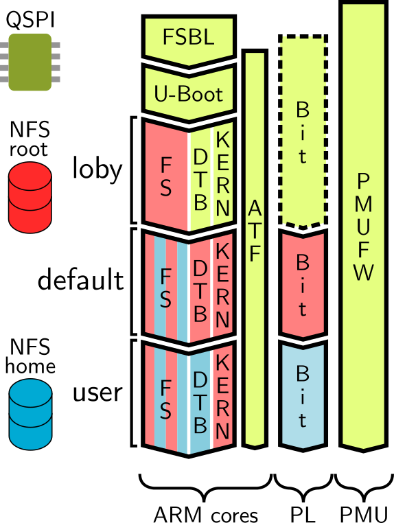
The development of a robust platform requires the customization of every component in the boot sequence. As existing tools were not efficient, we had to develop a custom tool, named YAT (Yet Another Tool), which automatically generates a boot image based on user profiles including the artifacts required for the initial booting stages (First Stage Boot Loader, U-boot, ARM Trusted Firmware, PMU firmware and Linux kernel). These binaries are aggregated into a single boot image, which is flashed into the QSPI memory attached to each MPSoC. An outline of the final boot process is presented in Figure 5. Optionally, this boot image can also incorporate the FPGA programming file, i.e. the bitstream, designated as ”Bit” in the figure.
Each platform user may have different FPGA programming firmware and software configurations. In order to support a multi-tenant architecture, these configurations have to be deployed swiftly onto the multi-FPGA platform, and in a manner that allows the sharing of the platform resources efficiently. Thus we developed a two-stage boot process. A first ”minimal” Linux kernel is loaded from local storage (QSPI flash memory), and mounts a root Network File System shared among all MPSoCs (”NFS root” in Figure 5). This share is read-only in order to improve the system security. Memory-based read/write overlays are created automatically for specific linux folders, to provide a read/write file system. Once the root File System (rootFS) is loaded, a script fetches a new set of binaries, initiates the execution of a second ”fully-featured” kernel through kexec (kexec, ), and optionally (re-)programs the FPGA. The second kernel loads the same rootFS, as well as a second share (NFS home in Figure 5), which contains the home folders of the users. Optionally, users may initiate additional stages to change the MPSoC configuration, without rebooting the whole board. In order to automate the development of new boot images with user configurations, YAT was extended to generate the so-called ”boot packages”, which packs together the kernel, Device Tree Blob (DTB) and the FPGA bitstream along with user boot packages.
In order to have a Linux distribution tailored to the needs of the ExaNeSt platform, such as the network connectivity and the booting environment, we created a Linux distribution, called Carvoonix and, which is based on Gentoo Linux. Carvoonix combines the flexibility of Gentoo and the convenience of distributions based on binary packages. In effect, a “builder” package distribution library is used for preparing, compiling and uploading optimized packages to a binary package repository, while a “deploy” package distribution library uses the binary repository for the final distribution. In case new packages are requested, we build and test them using the “builder” library and then make them available to the users through the “deploy” library. This increases the overall flexibility of the Linux environment.
Finally, the management of the QFDBs required significant effort. In order to support the ExaNeSt diskless environment, a management Virtual Machine (VM) was initially created. This VM provided the necessary network services (NFS, DHCP, DNS, NTP) to QFDBs as well as a user gateway functionality. By using a single management VM, the deployment of other QFDB-based systems was significantly simplified. However, as the platform grew larger, those functionalities were migrated to a physical machine in order to improve the performance. The NFS shares are backed up by a redundant ”ZFS” file manager pool. We implemented rolling snapshots at different time frequencies (from an hour up to a month), which proved to be very effective. Finally, ”Ansible” automation software was leveraged in order to manage large sets of QFDBs more efficient.
Overall, we have learned a lot during the development of the ExaNeSt platform. Foremost, we found out that deep knowledge across domains (electronics, FPGA firmware and system software) was merely a prerequisite. On many occasions, the tight collaboration between those fields of expertise has been crucial to the progress of the developments.
Eventually, our approach to the system boot software and management environment can be adapted to other prototypes, where flexibility and customizability at a medium scale are priorities. In effect, our approach automates the generation of all necessary FPGA firmware and software artifacts, as well as their selective deployment onto the system; while offering users a relatively stable work environment.
4. The ExaNeSt network communication
In this section, we present the ExaNet interconnect, developed in ExaNeSt and EuroEXA projects. We focus on the ExaNet Network Interface (NI), which is implemented in the Programmable Logic (PL) and connected to four (4) ARMv8 cores in the Programming System (PS) segment of the Xilinx MPSoC. The ExaNet also features (Torus) network routers that evolved from the APENET architecture (ammendola2004apenet, ).
The design principles behind the ExaNet interconnect are summarized below:
- •
-
•
Custom ”cell-based” switch interconnect in order to reduce latency,
-
•
Flow control for (nearly) lossless operation and congestion management to protect victim flows under congestive episodes, with shallow buffers inside the network core to reduce latency and cost (kornaros1998implementation, ; chrysos2015discharging, ),
-
•
Co-existence of compute and storage traffic over a converged interconnect (see Section 5.3).
4.1. Network Topology
The current topology of the ExaNeSt prototype is a 3D-Torus as depicted in Figure 6. The four Xilinx MPSoCs on a QFDB are fully connected through 16 Gb/s links, as shown on the right side of the figure. The ”Network MPSoC” (orange F1 block in the figure) is responsible for the external connectivity, as explained in Section 3.1. Only the firmware of the ”Network MPSoC” can route ExaNet packets to different destinations and thus the network traffic from the remaining three MPSoCs of the QFDB is first forwarded to the ”Network MPSoC”.
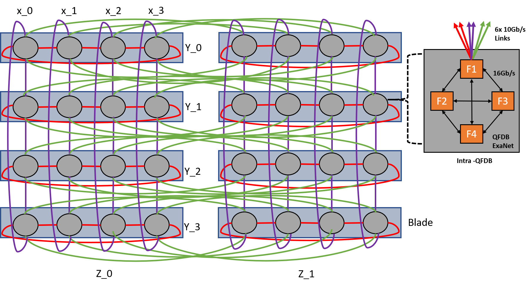
The four QFDBs inside a blade are connected in a ring topology through 10 Gb/s links on the X axis (red links). The QFDBs between four blades are also connected in a ring topology on the Y axis, as shown in the figure (purple links), creating a quad-blade group. Finally, the symmetrical QFDBs between two quad-blade groups are connected together as shown in the figure (green links).
A first implementation of the ExaNet network architecture is currently installed in the full-scale ExaNeSt prototype that comprises 8 blades, or 8x4x4x4 ARMv8 cores, and runs real HPC applications, using the custom MPI library, outlined in Section 5.2.1.
4.2. Overview of interconnect
Internally, the ExaNet interconnect features shallow buffers at network links (4 KBytes) and link-level flow control in order to avoid packet drops. The network packets (cells) are also small. Every cell carries up to 256 bytes of payload, split in 128-bit words. Additionally, each cell carries 32 bytes of control information used for transport, network routing, and link-level protocols, which is split in a 16 bytes header and a 16 bytes footer. The small packet size minimizes the latency of high priority traffic in front of busy links. We try to optimize the end-to-end latency, but we nevertheless perform store-and-forward when reading the payload of a cell from its source memory, in order to avoid memory-induced network hiccup, e.g. lines hitting in the cache subsystem may overtake older memory requests.
All switches and routers in ExaNet perform cut-through. In particular, there is a small input-queued switch in every FPGA to route packets between the local NI endpoints and the local links, with a latency of 2 clock cycles. Additionally, the network FPGA of each QFDB also contains a Network Router (ammendola2004apenet, ) with connections to remote QFDBs. The QFDBs are connected in a 3D-Torus topology through HSS links, as discussed in Section 4.1, and the Network Router guarantees deadlock freedom using single-path (dimension ordered) routing.
The ExaNet Network Interface (NI) offers two main primitives for user-level communication: 1) an RDMA engine, suitable for bulk remote-memory transfers; and 2) packetizer-mailbox pairs suitable for sending and receiving small messages with ultra-low latency. Regarding the connection of the NI with the ARMv8 cores and the host memory, we use a high-speed AXI-4 master interface that offers separate read and write channels (128-bit data width each). The NI and the switches implemented in the and Programmable Logic (PL part of our FPGA) run at 150 MHz, thus every read or write channels offers a raw memory bandwidth of 19.2 Gb/s. The base latency of a request round-trip between the PS (ARMv8 cores and memory subsystem) and the PL part of the FPGA ranges between 100-150ns, depending on the request. We have managed to saturate the paths to and from memory using eight (8) outstanding AXI burst transactions (16 x 128-bit words). All ExaNet links inside the FPGAs run at the same speed (128 bits at 150MHz), and incur an overhead of two words (header+footer) for every 16 words of payload (efficiency 16/18).
We have further explored the generic ExaNet architecture in order to implement and evaluate a number of novel technologies for interconnects such as:
-
(1)
End-to-end transfer resiliency in hardware, allowing to fully offload the CPU. Our reliable RDMA transport features dynamic connections, with fast (hardware-level) recycling of hardware contexts;
-
(2)
Fast completion notifications at the receiver, suitable for optimized MPI runtimes (ploumidisExacom, );
-
(3)
Accurate congestion management in hardware, replacing sub-optimal (software-based) solutions, such as TCP (giannopoulos2018accurate, ), (chrysos2015discharging, );
-
(4)
Page pinning avoidance by dynamically handling page-faults during RDMA transfers. For this purpose, we reuse the reliable hardware RDMA transport to replay faulting pages (psistakis2020part, ), (psis_tpds, );
-
(5)
Tightly-coupling new versions of the network interface with RISC-V cores (redsea2022, ).
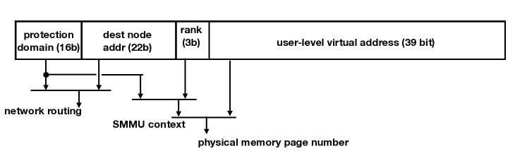
4.3. Global Virtual Address Space
All NI endpoints and memory locations inside the ExaNeSt prototype belong to a Global Virtual Address Space (GVAS) and can be addressed directly by any node through the interconnect. Figure 7 depicts the GVAS address, here used as a destination address of a network packet, i.e. the destination address of the first byte of the packet payload. An address in GVAS is 80 bits long. Part of the GVAS is used to route packets inside the physical interconnect, and part to identify a memory location within a node (belonging to some process). In order to route a network packet in the ExaNeSt GVAS, the packet address includes the following fields:
-
•
The protection domain id (PDID), 16 bits in the ExaNeSt prototype, is used by the hardware to check the initiator’s access rights on particular GVAS locations. The PDID carried by network packets mirrors the value set in special hardware registers by the system software. PDIDs allow the system administrator to create virtual groups of processes that can safely read and write their memory. With 16-bit PDIDs, we can have up to 64K process groups.
-
•
The destination node address, 22 bits, allows up to 4M nodes in the system. In principle, the node ID could also be virtual in order to allow process migration (katevenis2007interprocessor, ).However, in our current prototype we static map GVAS node IDs to physical nodes – i.e. endpoints of the interconnect.
-
•
The rank, 3 bits, is used to identify a specific local port, such as a peripheral/accelerator or a user-level process (e.g. MPI rank) with private memory space within a node.
-
•
The user-level virtual address, 39 bits, identifies a virtual address within a process, in the case of RDMA. Together with the rank, it can be used to compose a 42-bit node-level virtual address (VA).
4.4. ExaNet Lean Network Interface
The ExaNet network interface offers virtualized hardware blocks that support user-level initiated, protected transfers that completely bypass the kernel. Virtualization is provided by offering multiple channels that can be allocated to different processes. In this way, processes can safely initiate multiple concurrent transfers, without any kernel involvement. Eventually, the network interface serializes the requests from different applications, on a per-packet/cell basis.
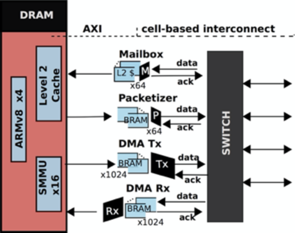
The main building blocks of the ExaNet network interface are depicted in Figure 8. The packetizer and mailbox primitives can be used for operations equivalent to remote store and load (from an incoming queue) operations, respectively. Simple remote store instructions cannot directly be routed in ExaNet. The packetizer-mailbox primitives that we use instead offer a reliable transport for small latency-sensitive messages.
Packetizer: The packetizer is a hardware block connected to the ARM core via an AXI-4 memory-mapped interface, and to the network using an ExaNet interface. It is virtualized, offering 64 virtual interfaces, each one accessible through a private memory page. Each interface further provides four (4) memory-mapped channels. Each channel can be used by the thread or process that owns the interface to transfer a packet and to monitor its execution by polling specific status bits in the page of the interface. Each channel can be in one of the following states: ongoing, acknowledged, negatively acknowledged, timed out. A user program stores the payload of the message into the channel address using (posted) store commands. In the final store command, the process writes the payload size and the destination address on a designated address of the channel, which prompts the packetizer engine to create a network packet, carrying the user-defined payload and the destination address, as well as the appropriate PDID.
Mailbox: The virtualized mailbox is a hardware block that includes 64 memory-mapped virtual interfaces. Multiple sources can concurrently write in the same mailbox interface. For ultra-low read latency, mailbox data that arrive from the network are written in the Level-2 cache (and main memory) of the ARM processor, utilizing a coherent (ACE AXI) interface between the PL and PS in the Xilinx MPSoC. The tail pointers of the incoming queues are maintained and updated in the FPGA (PL), while the head pointers are maintained and updated by the runtime. A process can request a new mailbox from a special driver, which allocates one mailbox interface and associates it with the process PDID. The process can then start polling for new arrivals as discussed in Section 5.2.1.
The mailbox hardware compares the PDID of incoming packets with the PDID of the targeted interface, generating a network negative acknowledgement (NACK) if these do not match. A NACK is generated also in case of packet error or full mailbox. Otherwise, the packet is enqueued into the virtual mailbox and an ACK is generated and routed to its source. The packetizer of the transfer maintains hardware timers, allowing the source to re-transmit the packet if the ACK is not received on time.
4.5. RDMA engine
For bulk transfers, we have developed an RDMA engine, which is optimized for zero-copy, user-level communication, and which can offload the host end-nodes from transfer-induced overheads. As shown in Figure 9, the Exanet RDMA engine consists of two main blocks, one at source node for reading data from memory and sending them to the network (Send unit), and one at destination node, responsible for receiving network data, writing them to memory, and generating end-to-end acknowledgments and completion notifications (Receive unit).
The Exanet RDMA Send unit offers 16 pages that can be allocated to different processes. Each page offers 32 write and 32 read channels (see Section 4.5.1). An RDMA write operation commences when a local process writes a 64-byte descriptor inside an available channel at the source node. The initiator must know the RDMA destination address, which must belong to a (remote) process with the same PDID. Special NI firmware running in the R5 co-processor of the MPSoC discovers new transfers, splits them in consecutive (16 KBy) blocks or transactions, waits for end-to-end acknowledgements. The R5 co-processor may re-transmit blocks that do not receive acknowledgement.
The transmission of individual blocks is handled by a hardware Send Engine, which splits blocks in cells. The hardware Send unit uses the SMMU (the ARM-based IOMMU available in our Xilinx MPSoC) for virtual address translation, and fetches the cell payload from memory, issuing an (IO-coherent) AXI-read burst operation inside ARM’s memory subsystem. In this way, data can be read from caches, thus obviating the need to flash caches before transfers. The Send Engine waits the entire payload from memory in order to inject the cell.
The Receive unit consists of a hardware engine, which forwards the payload of each incoming cell as it arrives from the network directly to its final memory destination. These AXI-write requests pass through the SMMU and the IO-coherence interconnect (see steps 3 and 4 in Figure 9). The Receive engine also maintains dynamic contexts in order to issue block-level acknowledgements and notifications.
4.5.1. RDMA Read
Our RDMA supports Read operations. Essentially, the issuer of the operation generates an RDMA Read Request and uses its packetizer to forward it to a special mailbox allocated to the RDMA Send unit in the node with the source data. The Send unit then allocates an available Read channel in the targeted page (protected by the PDID in the request), and completes the RDMA Read operation with an RDMA write. We use completion notification to inform the issuer that the Read data have arrived.
4.5.2. RDMA R5 co-processor
In the Exanet RDMA, a significant portion of the Sender unit is implemented through special firmware in the R5-Cortex co-processor IP of the Xilinx MPSoC. The premise of this approach is that the co-processor handles only transaction-level operations (initiation, ACK/NACKs re-transmissions), thus does not need to run at (cell) network speed. On the other hand, this software solution offered flexibility, development speed, and programmability benefits (paraskevas2018virtualized, ). Nevertheless, even our optimized R5 implementation consumes in 2-4 s every time it is invoked. This dominates the interconnect (and MPI) base latency. Inside the RED-SEA project, we redesign and implement these functions in hardware, which can now handle small transfers in back-to-back cycles while reducing the base latency of RDMA operations well below 1s.
4.5.3. SMMU & No page pinning
In ExaNet, we handle page faults that may occur in RDMA transfers dynamically using special software and hardware at the endpoints, in order to re-transmit blocks that experienced page-faults. In this way, there is no need to pin pages prior to transfer; in turn, this allows to expose the full address space of applications through RDMA operations (psistakis2020part, ; psis_tpds, ). Instead of designing a custom hardware for memory address translations at source and destination nodes, we reuse the ARM System Memory Management Unit (SMMU) (ZynqTRM, ). The SMMU is provided by ARM, but, operation-wise, is similar to other IOMMUs. Traditionally, IOMMUs are responsible for memory requests to and from I/O devices that are memory-mapped to special (pinned to memory) virtual memory regions. In ExaNet, we reuse ARM’s SMMU for accesses coming from the network.
As shown in Figure 9, a SMMU in source and destination nodes is in charge of the address translation of global virtual addresses to local physical memory addresses (PA), as also described in Section 4.3. For this to work, we had to ”convince” the SMMU to use pointers to process page tables inside the SMMU channels (context banks). Effectively, the SMMU hardware walks and fetches translations from the OS page tables of user processes. The SMMU further includes a Translation Lookaside Buffers (TLBs) for recent page translations. Similar to a CPU TLB miss, a SMMU (TLB) miss can be handled by the hardware Page Table Walker without any software (or OS) intervention if there is no page fault. In case of page-fault, the SMMU generates an interrupt which is handled by OS modules.
4.6. Hardware complexity of ExaNet Network Interface
The hardware resources required by the Network Interface in the Xilinx FPGA are minimal. The Packetizer and the Mailboxes consume 20K FPGA LUTs (5.5%) and 8 FPGA BRAMs (1%) (ZynqTRM, )111Mailbox payload buffers are implemented in host memory.. The RDMA engines of the Send and Receive units consume 33K LUTs (12%) and 19 BRAM blocks (2%)in total.
4.7. Allreduce accelerator
Another important component of the Network Interface is an accelerator for the MPI_Allreduce collective primitive. The accelerator was implemented with Xilinx Vivado High-Level Synthesis and is currently able to handle the following cases:
-
•
Sum, min, max arithmetic operations
-
•
Int, float, double datatypes
-
•
Up to 1024 MPI ranks
-
•
Vector size up to 256 bytes (Bigger vector sizes require multiple operations on 256-bytes vectors)
-
•
At most 1 MPI rank per FPGA/SoC
-
•
Whole QFDBs must be part of the Allreduce operation, i.e. the total number of MPI ranks must be a multiple of 4
For other use cases, the Allreduce primitive is handled in software through the algorithms supported by ExaNet-MPI (Section 5.2)
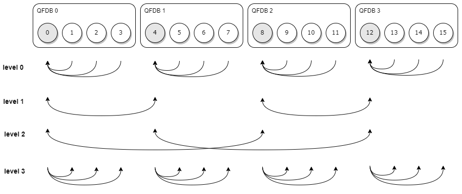
For the purposes of our implementation and by taking into account the unique properties of our system, we came up with an Allreduce algorithm tuned specifically to QFDB characteristics. The algorithm tries to minimize a) the network traffic between the nodes involved and b) the processor Network Interface interaction. In effect, those interactions take place only at the beginning and at the end of the Allreduce operation, while all the arithmetic calculations and communication patterns are performed and determined inside the hardware. Moreover, we designed 2 distinct modules in the accelerator, in order to minimize the intra-QFDB traffic and optimize the inter-QFDB communication. The Allreduce client module resides inside all FPGAs but ’Network’ FPGA. It is responsible for fetching and sending data to the ’Network’ FPGA at the beginning of the Allreduce algorithm and updating the software at the end of the operation. The Allreduce server resides only in the ’Network’ FPGA and is responsible for inter-QFDB communication and for performing arithmetic calculations. This algorithm is illustrated in Figure 10 for an example of 16 ranks. Overall, the implemented Allreduce algorithm is the following:
-
•
Initialization: At the beginning of an Allreduce operation, the software programs every module with the arithmetic operation type, datatype, vector size. Two pointers are also provided, one with the memory address of the data and one with the memory address of the table that contains the {MPI rank, network address} pairs. The rest of the algorithm can be visualised as a graph of levels, where is the number of ranks involved in the Allreduce collective.
-
•
Level : Each module performs a DMA operation to fetch its own vector from the local memory. The client modules send their data to the server module in the ’Network’ FPGA; and the server module calculates the reduced vector for all the MPI ranks that reside in that QFDB.
-
•
Levels to : Each server module exchanges its local vector with another server module, and performs reduction with its own local vector. With each level, the rank difference between the servers increases as a power of two (i.e., 4,8,16,32,etc). At the end of level , each server module has calculated the final reduced vector of all the ranks that take part in the Allreduce operation.
-
•
Level : The server module broadcasts the vector to its intra-QFDB client modules and each module updates the memory with the reduced vector and notifies the software that the Allreduce operation has completed.
5. The ExaNet system software
Apart from the development of the ExaNeSt hardware platform, the custom interconnect and the network interface, significant effort was also put on developing and tuning the system software stack. The main goal was to derive runtimes that efficiently take advantage of all the hardware capabilities while addressing any potential platform limitation. Along this direction, HW components of the ExaNeSt network interface and SW components of the system software were codesigned. For example, in order to support efficient remote data transfers the system software should take advantage of the HW primitives of the ExaNet network interface, which was designed based on the requirements of the applications.
5.1. ExaNet user-space communication API
At the top of the ExaNeSt system software stack, the ExaNeSt user-space communication API allows user-level access to the hardware blocks of the network interface (see Section 4.4), such as, the RDMA engine, the virtualized packetizer and the virtualized mailbox. The simple hardware blocks of the network interface allow for a minimal but efficient user-space API, as shown in Section 6.
The virtualized mailbox/packetizer hardware blocks, that are accessed through the user-space API, offer the capability of user-level low-latency atomic message delivery. In particular, the API provides to runtimes and user applications the functionality for allocating virtual interfaces of the virtualized mailbox and packetizer that reside on the local compute node. The linux kernel is only involved in the allocation/deallocation of virtual interfaces. The kernel driver that is responsible for the mailbox gives direct access to user applications to a specific set of hardware registers. By using this set of registers, the applications can directly send and/or receive small messages to/from remote processes in user space. In this way, the actual data transfers are initiated at user-level without requiring any kernel involvement. The API allows applications to atomically send messages of up to 64-bytes to any virtual interface (or process address) of any remote node. Furthermore, if an application has acquired an interface of the virtualized mailbox, it can receive messages sent by remote nodes of the same protection domain. The messages generated by the packetizer wait for an end-to-end acknowledgment, and can be re-transmitted after the expiration of a timeout period.
This API also allows applications and runtimes (e.g. MPI) to perform RDMA protected transfers between local and remote virtual addresses. The API for RDMA is quite minimal, providing calls for accessing a remote virtual address, inserting a descriptor, and polling for completion. Both RDMA read and RDMA write operations are supported.
5.2. Low-overhead runtimes
5.2.1. The ExaNet-MPI runtime
MPI is the de facto standard for a large number of parallel HPC applications, allowing to efficiently exploit the resources available on modern HPC systems. Thus, a major component of the ExaNeSt system software is a custom, platform-specific MPI library that takes advantage of the features of the ExaNet interconnect. We have developed the ExaNet-MPI runtime, which partially implements the MPI standard, including almost all point-to-point and collective primitives. However, its current version lacks support for RMA operations and non-blocking collectives. The ExaNet-MPI runtime implements all the primitives required by the MPI microbenchmarks and applications that were used for the platform evaluation, while it does not support rarely used primitives (e.g. MPI_Scan, persistent requests). Collectives where implemented using the same algorithms that were used by MPICH, version 3.2.1.
The ExaNet-MPI was designed to take advantage of the features provided by the ExaNet network interface in order to improve performance. In particular, it takes advantage of the capabilities of the virtualized mailbox and packetizer to offer efficient atomic, low latency message delivery required by latency sensitive traffic, such as, control messages for MPI protocol handshaking, as well as, acknowledgments. Moreover, the packetizer can be used for eager data transfers in order to send directly payload or control data in a single message instead of using the RDMA engine. In the current ExaNet version, the maximum payload size that can be send from a packetizer to a mailbox is bytes. ExaNet-MPI also takes advantage of the high bandwidth RDMA engine, described in Section, and specifically its capability to deliver a completion notification in parallel with the actual data. This notification can be sent to any virtual address.
The key feature of the network interface that ExaNet-MPI exploits, is that the mailbox, the packetizer and the RDMA engine are virtualized and thus they allow for user-level data transfers. This is implemented using the ExaNet communication API, described in Section 5.2, which provides to the upper layers (i.e. the MPI runtime) of the system software user-level access to the NI hardware blocks. In this way, the kernel is involved only in the initialization of a transfer and not in the actual data transfer, avoiding the overhead of system calls, which may become an important performance bottleneck.
In order to implement the ExaNet-MPI runtime we considered two different approaches. The first one was to modify a well known MPI implementations, such as OpenMPI (4100410, ) or MPICH (GROPP1996789, ), in order to support the ExaNet communication API. For the OpenMPI runtime, this approach would require the development of a new byte transfer layer (BTL) that uses the API to transfer traffic through the ExaNet network interface. Moreover, this approach would require extra effort to experiment with different messaging protocols for the point-to-point messages. The second approach, which was eventually followed, was not based on any existing MPI implementation. Instead, ExaNet-MPI consists of two different libraries, one that implements the MPI point-to-point (pt2pt) primitives and one that implements the MPI collective functions using the point-to-point primitives. Any primitive that is not implemented is delegated to an MPICH library (version ). The only modification required to this library was to export the context ID of a communicator in a 16bit value. This was needed since packetizer messages have limited space for control data. This approach gave us more flexibility to experiment with different implementations and protocols, such as different versions of the rendez-vous protocol for pt2pt messages.
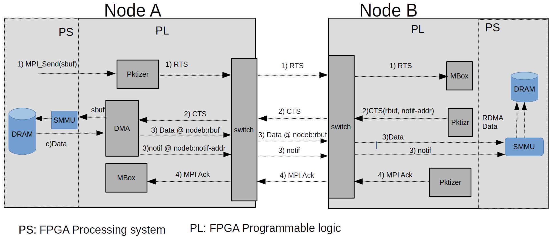
Figure 11 depicts the hardware blocks and the message exchanges involved in the ExaNet-MPI rendez-vous protocol. The scenario in the figure includes the communication between an MPI process A running on node A and an MPI process B running on node B. In this scenario, process A issues an MPI_Send before process B issues the corresponding MPI_Receive. The buffer that contains the data of the sender is denoted as sbuf. First, on the sender’s side, the pt2pt library sends a request-to-send (RTS) message that includes control information, such as, the data size of the MPI transfer, the communicator, the source and the destination rank. The RTS message is sent through the sender’s packetizer to the receiver’s mailbox. In step 2 of the figure, when the matching receive is posted, ExaNet-MPI on the receiver’s side, sends a clear-to-send (CTS) message that specifies the virtual address of the receiver buffer (rbuf) for the data transfer and the virtual address (notif-addr) of the transfer completion notification that process A should send to process B. The notif-addr address can be any virtual address of the receiver process. The CTS is also a small message, which is sent through the packetizer and targets the mailbox of senders’s RDMA. In step 3 of Figure 11, process A setups the RDMA transfer in order to write the data in the receiver’s buffer (rbuf). Note that rbuf is preprocessed in order to incorporate information that indicates the target node transforming it into a remote virtual address. The same applies to the virtual address provided by the receiver where the completion notification should be sent. Let us also note that, data issuing and notification delivery take place concurrently. On node A, the System MMU (SMMU) translates the virtual address of the sender’s sbuf buffer address to physical address (also explained in Section 4.5). On node B, when the request to access the remote virtual address enters the receiver’s network interface logic, any information related to the node id is removed while the virtual address of the receiver’s rbuf buffer is translated to physical address through the SMMU. Once process B has sent the CTS message, it can periodically poll the notification address for the completion notification. When the notification arrives, the receiver issues an acknowledgment back to the sender, in step 4 of the figure, and the message exchange completes.
The point-to-point protocol described in the aforementioned scenario is sender-initiated and is actually read-based with read being emulated through a DMA write from the receiver. We are currently evaluating a write-based variant of the rendez-vous protocol that is both sender- and receiver-initiated with matching also taking place at both sides.
5.2.2. The GSAS environment
GSAS (GSAS, ; GSAS2, ) (Global Shared Address Space) is an efficient and flexible shared memory abstraction on top of the ExaNeSt platform. The GSAS environment defines an application programming interface (API) that provides a shared memory abstraction model to distributed applications. More specifically, GSAS gives the ability to processes running across remote servers/nodes to communicate in a way resembling a system that provides coherent shared memory communication. It allows the applications to allocate/de-allocate memory (local and remote), and to perform several atomic operations (i.e. read, write, Fetch&Add, etc.) on the allocated space by using the appropriate API calls that the environment provides. The API of GSAS provides most of the functionality that PGAS languages and runtimes provide. The current implementation of the GSAS environment uses a minimal set of hardware primitives for efficiently supporting the use-case of a shared memory abstraction on top of message passing system.
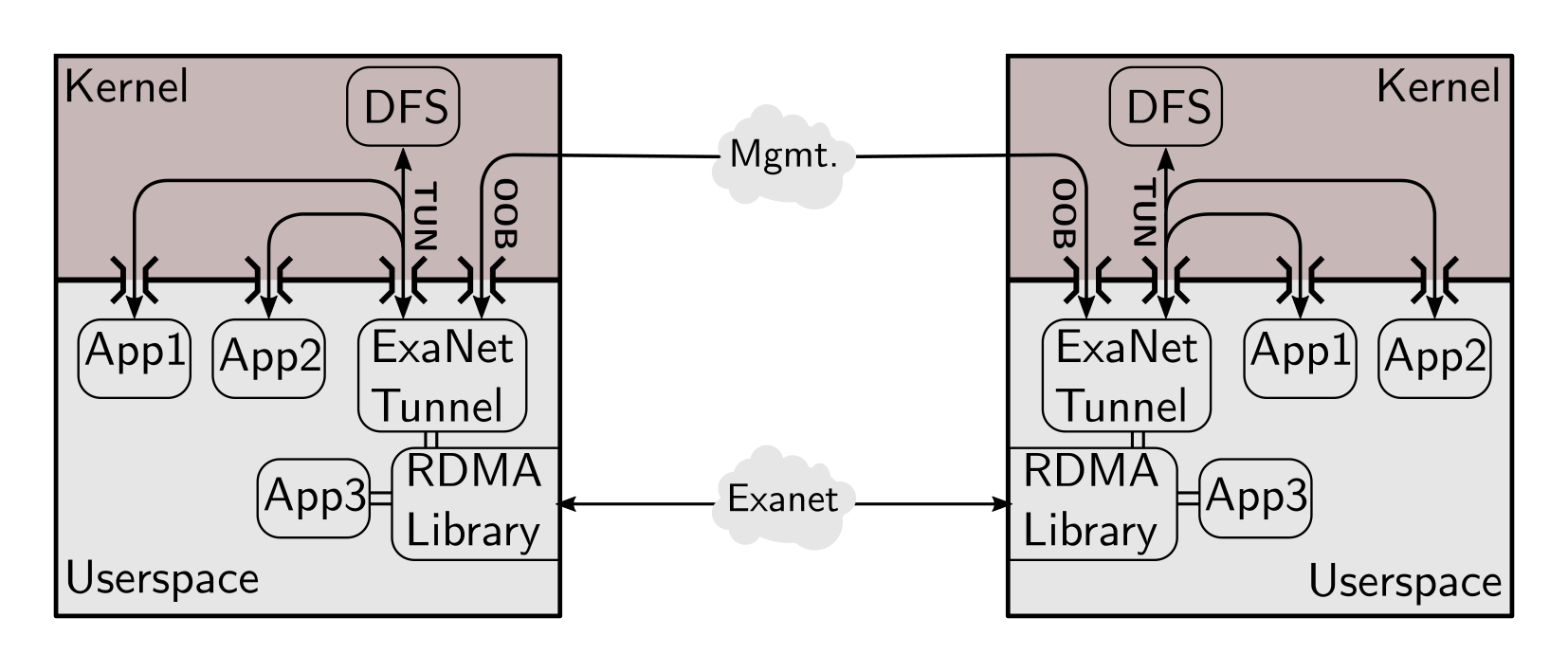
5.3. IP-over-ExaNet service
While the focus of this testbed is on HPC runtimes that directly instantiate RDMA transfers, some applications and services typical to HPC systems demand legacy networking interfaces. Primarily, Distributed File Systems (DFS) are implemented in the kernel, or, rely on socket semantics to perform communications. There is also a variety of management services such as resource management or monitoring that may suffer from the management network limitations in large systems. As a consequence, modern HPC systems strive to adapt their High-Performance fabric to also support legacy socket interfaces, which leads to the convergence of a variety of applications and services onto the same network.
In order to support those socket-based services, we built a minimal IP overlay on top of the ExaNet interconnect presented in Section 4. The architecture of our solution is presented in Figure 12. For sake of simplicity, this service is implemented by a user-space program that tunnels packets between the Linux kernel and the ExaNet fabric. In order to deal with the lifecycle of nodes robustly, Out-of-Band (OOB) communication is established using the Ethernet Management Network upon start. Each node regularly emits an heartbeat message and reacts to messages from other nodes.
Once a remote node is detected, receiving and transmitting buffer rings are allocated by the user-space program, and a handshake takes place using the ExaNet interconnect. Afterwards, IP packets are transferred over the ExaNet fabric, from the transmitting buffer of an endpoint to the receiving buffer of the other endpoint. In order to improve performance, multiple packets may be sent in a single RDMA transfer, and we leverage the RDMA notification mechanism to efficiently synchronize the transmitter and the receiver. Finally, it is worth noting that we take advantage of the properties of the ExaNet fabric (data protection, in-order reliable delivery) to reduce the burden on the CPU cores.
In order to interact with Linux kernel networking, the program instantiates a TUN socket, which allows simple user-space programs to act as a complete IP interface. Hence, the Linux kernel routes packets into the user-space program and packets received by the program are forwarded into the kernel. In this implementation, we relied on the and system calls. With newer Linux kernels, liburing may be leveraged to improve performance.
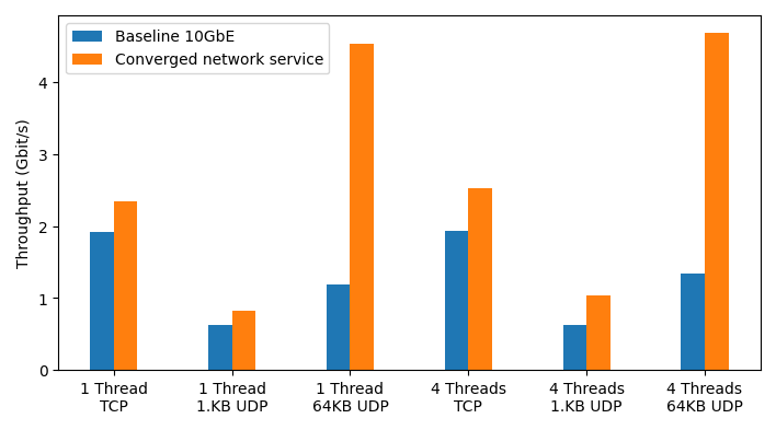
In order to assess the performance of this solution, we used two nodes with a network distance of 5 hops, and we compared with the 10 Gigabit Ethernet management interface. It is important to note that both management interface links and cross-QFDB ExaNet links have the same lane rate (10Gbit/s). For throughput measurements, the iperf3 benchmark was used. Results are presented in Figure 13. The converged network service consistently offers better throughput. In particular, for large UDP packets, our solution achieves a throughput of 4.7 Gb/s while the baseline reaches only 1.3 Gb/s. Latency-wise, the structure of our solution hinders its reactivity to sporadic messages. When the user-space program actively polls for incoming messages, average Round-Trip Time (RTT) is 90 s; while baseline average RTT is 72 s. Another approach relies on adaptive sleep periods to provide very similar throughput with much smaller processing core usage. However, in that case, average RTT reaches 2.2 ms; which might be prohibitive for delay-sensitive applications.
6. Evaluation
In this section we evaluate the performance of the ExaNet communication infrastructure. The evaluation includes results from microbenchmarks to real-world MPI scientific applications, using the MPI runtime described in Section 5.2.1.
We first employ point-to-point based microbenchmarks, from the OSU suite (osumicrobenchs, ), to explore latency and bandwidth for the different types of links and paths available in the platform. From the OSU suite, we also employ the broadcast and allreduce collective microbenchmarks. Both of them are used as a first step towards assessing how performance scales with an increasing number of processes. The allreduce benchmark is also used to measure the performance benefit of the allreduce accelerator that was presented in Section 4.7. We further explore how the performance of the MPI runtime and the platform scales through two MPI applications and a miniapp. Miniapps are relative short codes that are aimed to capture key application performance characteristics (jcc2015, ). For all of them, we perform weak and strong scaling tests. MiniFE is a miniapp from the Mantevo project (minifetechreport, ), that mimics the finite element generation, assembly and solution for an unstructured grid problem. Several scientific problems require the formulation of a nonlinear system of equations, which in turn is solved by a Conjugate Gradient solver. In that sense, miniFE is representative of MPI applications targeting such problems. The first application measured is LAMMPS (LAMMPS, ). This is a widely-used tool for particle-based modeling of materials at scales ranging from atomic to mesoscale, to continuum. The next MPI benchmark used is HPCG. HPCG (doi:10.1177/1094342015593158, ) is intended to provide a new metric for HPC systems ranking and constitutes a complement to the High Performance LINPACK (HPL) benchmark. It generates a synthetic discretized three-dimensional Partial Differential Equation (PDE) model problem, and computes preconditioned Conjugate Gradient iterations for the resulting sparse linear system. PDEs are also common in various scientific problems. Thus, the computation and communication patterns generated by HPCG are also representative of various scientific applications.
6.1. Microbenchmark-level results
6.1.1. Osu latency
First, we focus on the ExaNet interconnect latency and bandwidth, across different paths with different number of hops and different types of links in the ExaNeSt platform. Thorough deployment of the microbenchmarks is quite important, since deriving accurate performance measurements for complex large scale systems is challenging (1592958, ; 7426807, ; 4536494, ). As mentioned above, we used the OSU microbenchmarks suite (osumicrobenchs, ). Benchmarks in this suite have several desirable features. First, they perform a set of warm-up MPI operations in order to discard any machine setup overheads. For the case of MPI collectives, these benchmarks issue a barrier before calling the MPI collective primitive to synchronize the process execution (4536494, ; 7426807, ). Finally, each benchmark is executed several times in order to analyze variances in performance and identify deviations over time (7426807, ). These benchmarks are compiled and executed in the MPI runtime environment presented in Section 5.2.1.
| Type | Number | HSS Links | Example |
|---|---|---|---|
| of hops | & Capacity | ||
| ⓐ Intra-QFDB-sh | 1 | Gb/s | M1QAF1 - M1QAF2 |
| ⓑ Intra-mezz-sh | 1 | Gb/s | M1QAF1 - M1QBF1 |
| ⓒ Intra-mezz-mh(2) | 2 | Gb/s Gb/s | M1QAF1 - M1QBF2 |
| ⓓ Intra-mezz-mh(3) | 3 | Gb/s Gb/s | M1QAF2 - M1QBF3 |
| ⓔ Inter-mezz() | Gb/s | MmQAF1 - MnQAF1, | |
| Gb/s |
In Table 1, we list the different types of the evaluated paths. The ExaNeSt MPSoCs, as referenced in the ”example” column, are named denoting the mezzanine index, the QFDB index, and the MPSoC index. For example, M1QBF1 corresponds to the network MPSoC (F) of the second QFDB (QB) on mezzanine one (M). The row ⓐ corresponds to a path between two MPSoCs on the same QFDB (Intra-QFDB). In effect, since all network traffic inside a QFDB is routed directly (see Section 4.1), we have only single hop paths for each MPSoC of a QFDB. The links connecting MPSoCs within a QFDB are 16 Gb/s serial links. Paths ⓑ-ⓓ listed in the table (Intra-mezz) correspond to paths between MPSoCs that reside on the same mezzanine but on different QFDBs, connected through 10 Gb/s serial intra-mezzanine links. For example, the single-hop path Intra-mezz-sh corresponds to a link between the network MPSoCs of two different QFDBs on the same mezzanine. A path between two MPSoCs other than F includes both intra-QFDB and inter-QFDB links. For example, the path from M1QAF2 to M1QBF3 corresponds to entry ⓓ (Intra-mezz-mh(3)) as it includes an intra-QFDB link between M1QAF2 and M1QAF1 (F2-to-F1), one intra-mezzanine 10 Gb/s link between M1QAF1 and M1QBF1 (QA-to-QB) and an intra-QFDB link between M1QBF1 and M1QBF3 (F1-to-F3). Paths across mezzanines include at least one inter-mezzanine 10 Gb/s link. The last table entry (ⓔ) shows a generic path between two MPSoCs that includes inter-mezzanine, intra-mezzanine and intra QFDB links.
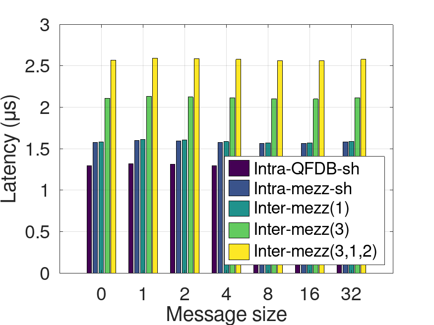
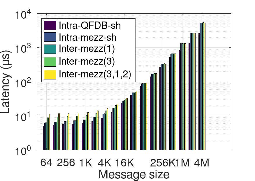
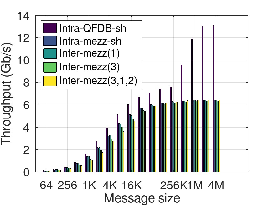
Figure 14 shows the network latency between two MPSoCs for various paths and message sizes, using the osu_latency microbenchmark. Small messages of up to 32 bytes are transferred using the ExaNet-MPI eager data transfer protocol, which involves only the packetizer and the mailbox, as described in Section 5.2.1. For single-hop paths between two MPSoCs within a QFDB, the latency of an empty message (i.e. the payload size is 0) is s. Messages of up to bytes have a latency lower than s. This includes MPI-related processing, such as management and recording of MPI transactions, on both endpoints; as well as the delay to transfer the message from main memory of the sender to main memory of the receiver. At the source node, the message has to be copied from the main memory to the packetizer; while at the destination node, the message has to be copied from the mailbox to the main memory. Using the Xilinx Chipscope logic analyzer core and tool (xchipscope, ), we have measured ns (approximately FPGA clock cycles) for each such copy operation on the ZU9EG MPSoC. The remaining message transfer time includes the time for the packetizer initialization, the link latency and the link transfer time. The duration of the physical transfer of messages of a few bytes is negligible. In order to measure the link latency more accurately, we ran the osu_latency benchmark with two MPI ranks on the same MPSoC. The measured latency includes all the above mentioned components but the link latency, since the message is transferred inside the same MPSoC. The latency of an empty message is s and thus the link latency is about ns (-). The time consumed by the MPI-related processing is quite noticeable because the ZU9EG MPSoCs incorporates slow in-order ARM Cortex-A53 cores. Moreover, the latency is further affected by the long hardware path between the CPU and the memory controller inside the MPSoC. Overall, the execution time of the MPI-related processing depends on the processor speed and the implementation of the MPI library; while our main focus is on the optimization and evaluation of the ExaNet interconnect, including the Network Interface described in Section 4.4. Therefore, we created a custom micro-benchmark that directly performs a ping-pong message test directly from user space, without any kernel intervention, utilizing the packetizer of the sender and the mailbox of the receiver. Direct access to these hardware blocks is achieved through the user-space libraries discussed in Section 5.1. In these tests, ping-pong messages are transmitted between two adjacent MPSoCs on the same QFDB. The average measured one-way message latency was around ns. Another interesting observation is that the average latency increases from s for bytes to for bytes. In effect, small messages go through the packetizer, which supports payloads up to bytes. Larger messages are sent using the RDMA engine, which incurs various overheads. The rationale is that those overheads are amortized for larger transfers. Furthermore, we have compared the latency between two adjacent MPSoCs on the same QFDB (Intra-QFDB-sh path) with the latency between two adjacent MPSoCs on different QFDBs on the same Mezzanine (Intra-mezz-sh path). For a message of zero bytes, which carries only control data of the MPI protocol, the corresponding latencies are and s respectively. The reason for this discrepancy is that the router for the communication of the MPSoCs on different QFDBs is slightly more complex, since it supports network deadlock avoidance, and thus incurs slightly higher latency (approximately ns).
We further measured the single-hop communication latency, which includes the inter-mezzanine link latency and the message processing required by the routing logic, between two MPSoCs on different neighboring mezzanines. The measured communication latency is about ns. Note that, for a path of intra- or inter-mezzanine hops, the message passes through MPSoCs and thus through ExaNet hardware switches, which are responsible for routing the packets. Based on the measured results, we have derived that the approximate link latency is ns, and thus the ExaNet routing block latency (denoted as ) is approximately ns. Also, the link latency and the ExaNet switch latency () are almost the same for intra- and inter-mezzanine single-hop paths.
We have next analyzed and measured the latency of an empty message transfer over the shortest and over the longest ExaNet paths shown in Figure 14. The right-most bars depicted in this figure correspond to the latency of a path that consists of three inter-mezzanine hops over 10 Gb/s links, one 10 Gb/s intra-mezzanine link and two 16 Gb/s intra-QFDB links (denoted as Inter-mezz(3,1,2)). The latency for an empty message over this path is s. Based on the aforementioned measured results, the expected latency over this path is s, where is the link latency. Note that s is the part of the intra-QFDB single hop latency excluding only . In the previous equation, term refers to the latency contributed by the two intra-QFDB hops. Thus, the expected latency over the aforementioned path is s, which accurately matches the observed value.
Finally, we have measured the latency of large messages using the OSU microbenchmark. The latency of a bytes message over an intra-QFDB path is s, while the corresponding latency of a MBytes message is s, which implies that the throughput achieved by the DMA engine (discussed in Section 4) is approximately Gb/s. This result matches the osu_bw throughput reported by the benchmark, as explained below. As a brief overview, Table 2 summarizes osu latency results derived through ExaNet-MPI and the case of zero byte messages. Apart from the paths listed in Table 2, we also list the case of a path that consists of a single hop inside the same FPGA.
| Type | Num of osu_latency (s) |
|---|---|
| ⓐ Intra-QFDB-sh | 1.293 |
| ⓑ Intra-mezz-sh | 1.579 |
| ⓒ Intra-mezz-mh(2) | 2 |
| ⓓ Intra-mezz-mh(3) | 2.111 |
| ⓔ Inter-mezz(3,1,2) | 2.555 |
| ⓕ Intra-FPGA | 1.17 |
6.1.2. Osu bandwidth and bidirectional bandwidth
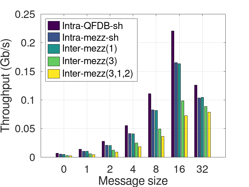
Figure 15 plots bidirectional bandwidth results from the osu_bw microbenchmark. Similar to the case of latency, we consider the different paths listed in Table 1. As expected, the capacity of the link is under-utilized for small messages. First, in addition to the actual payload, each message carries control information, such as the MPI tag, size, and communicator. The size of this control information is negligible in large messages that may include MBytes of payload; but not so for sizes presented in Figure 15(a). Additionally, each message exchange that follows the rendez-vous point-to-point protocol requires some control packets, such as, Request-to-Send (RTS) and acknowledgements. For a Intra-QFDB-sh path, a single 16 Gb/s link is traversed. For the largest message size of MBytes, the measured throughput is approximately Gb/s. This corresponds to a theoretical link utilization equal to . For single-hop inter-mezzanine links, the link capacity is Gb/s and the throughput achieved for messages of MBytes is Gb/s which corresponds to a link utilization. This noticeable disparity in the link utilization is due to the ExaNet routing logic between different QFDBs, which transfers some control data along with each data packet, mostly for implementing flow control. The overhead of control data would be negligible in large ExaNet packets. However, we have decided to use ExaNet packets of up to bytes in order to favor the latency over the throughput, since the latency is paramount for small control messages.
We have also run the osu_bibw microbenchmark for the same paths, where both sides send messages to each other. The benchmark measures the the maximum sustainable aggregate bandwidth between two processes (osumicrobenchs, ). Each side first issues multiple MPI non-blocking receive requests and then multiple MPI non-blocking send requests for a batch of messages. It then waits for these transfers to complete before proceeding to a new batch of requests. For message sizes of to MBytes, the throughput reported by osu_bibw is almost twice the corresponding value reported by osu_bw. This is expected since the high-speed serial links connecting MPSoCs, QFDBs and mezzanines are bidirectional. There are some small deviations though because of the sharing of the ExaNet routing logic resources and memory subsystems by both sides. As an example, for a message of Mbyte and an Intra-QFDB-sh link, the throughput achieved by osu_bibw is lower than the expected value based on osu_bibw. For small messages, where the size of the control information is comparable to the size of the payload, this deviation can become as large as nearly , while for an mid-size message of over an Intra-QFDB-sh link it is . Finally, the difference of the osu_bibw throughput from the expected value, based on osu_bibw, follows similar deviations regardless of the type of the ExaNet path involved in the test.
6.1.3. Osu collective microbenchmarks
The results reported so far concerned benchmarks that use point-to-point MPI primitives to exchange traffic. Results from the osu_bcast benchmark that uses the MPI_Bcast primitive (i.e. message broadcast) will be now presented. As already discussed in Section 5.2, part of ExaNet-MPI is a library that implements collective primitives on top of point-to-point ones. For the case of broadcast, a binomial tree is used. In Figure 16, we present average broadcast latency for different message sizes and different number of ranks. For deriving the average latency, different executions were conducted for each setup. We spawn one process per MPSoC, so the maximum size setup contains processes, involving all eight mezzanines of the current prototype.
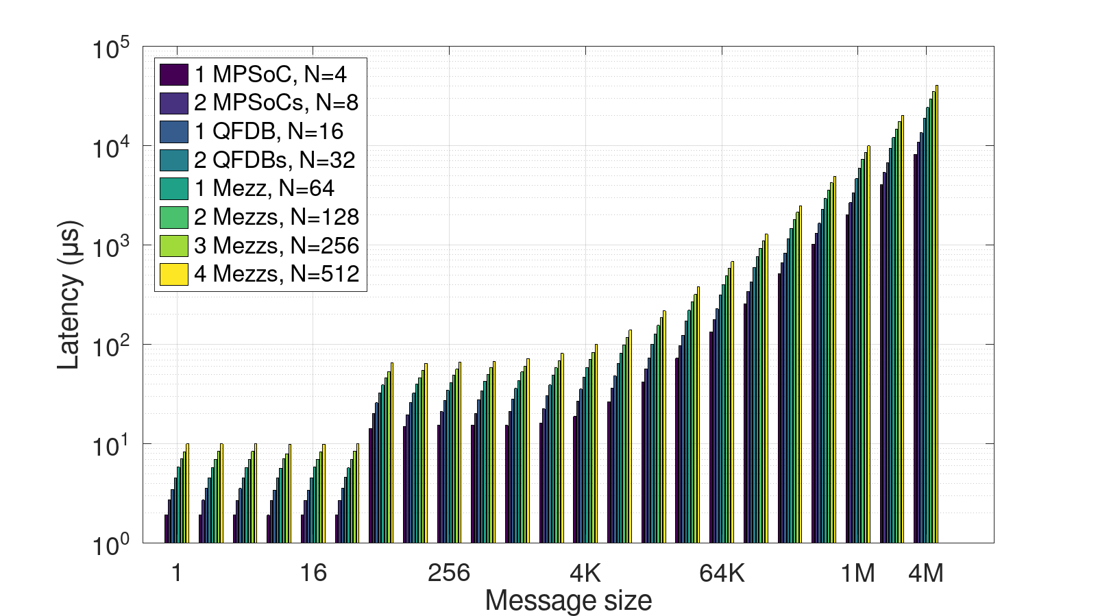
Since broadcast is unrolled as a loop of point-to-point exchanges in ExaNet-MPI, there are two discrete groups of measurements for all different setups. For messages up to bytes, the eager protocol is used and so latency for such messages is noticeably lower than for larger messages. For the case of byte long messages and processes, average broadcast latency is s. Similar latency values are observed for all messages up to bytes, since they are transferred through a single message in accordance to ExaNet-MPI’s eager protocol. For messages up to or kilobytes, transfer time is dominated by RDMA startup latency. For larger messages though, doubling message sizes also resulted in doubling broadcast latency.
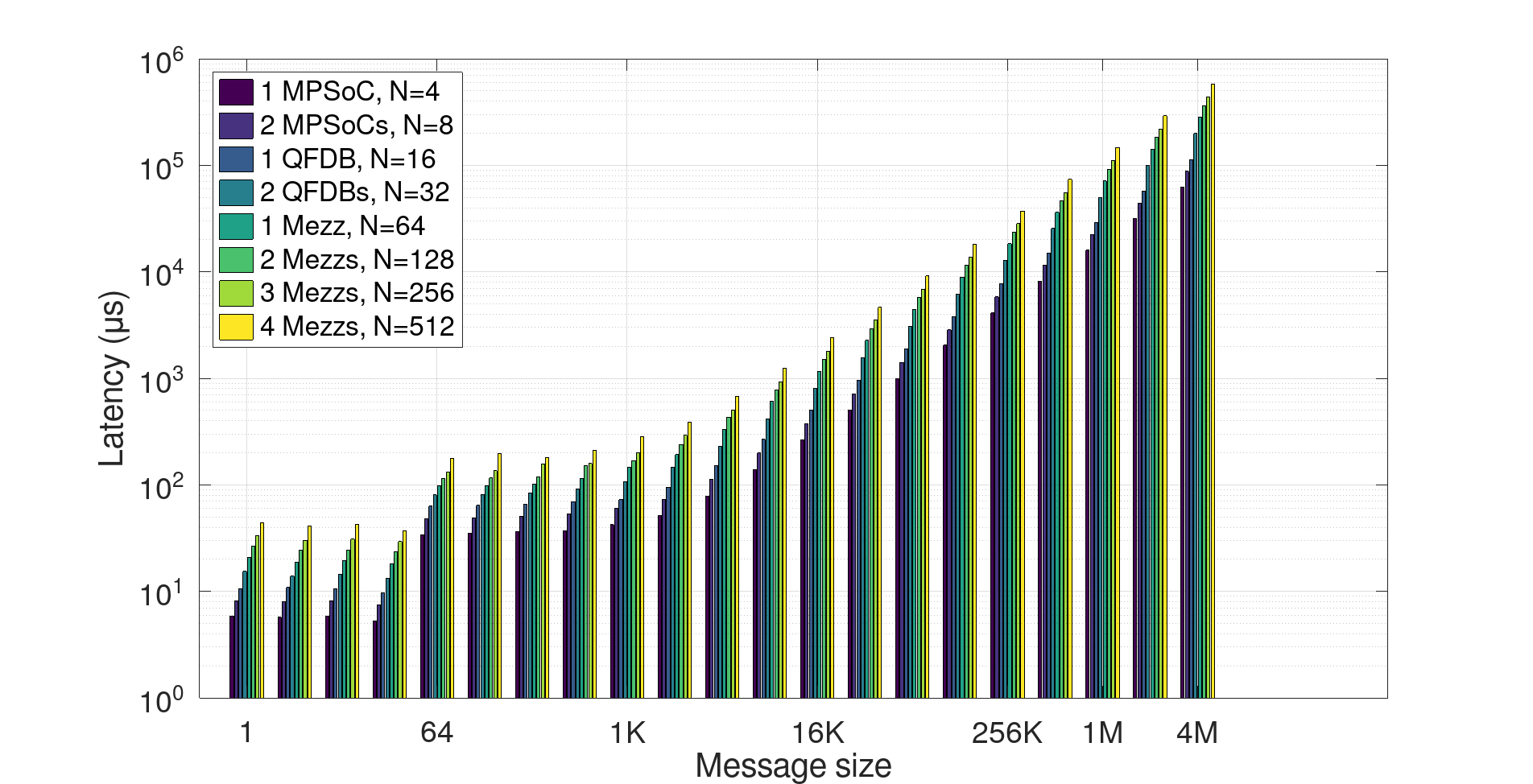
The last microbenchmark considered is osu_allreduce. The allreduce primitive in ExaNet-MPI is implemented through the recursive doubling algorithm, which performs an MPI_sendrecv call followed by an MPI_Reduce_local for every scheduled step. Apart from the communication, it also requires allocation of a temporary buffer where intermediate allreduce results will be stored. Finally, it requires one memcopy at the beginning to populate the intermediate buffer with the contents in the send buffer, and a second one at the end to store the final output in the receive buffer. Figure 17 depicts average osu_allreduce latency (over 30 different executions) for a different number of participating processes. Allreduce latency for the case of ranks residing on the same QFDB is s. The corresponding value becomes s for the case of byte messages. The reason is again that point-to-point primitives switch to the rendez-vous protocol for message sizes larger than bytes. As opposed to the eager protocol, the rendez-vous one relies on the RDMA engine for message transfers, which exhibits slightly higher startup latency. Compared to the corresponding broadcast latency for ranks, it is slightly higher due to the MPI_Reduce_local and the memcopies involved.
6.1.4. Osu broadcast performance scaling
Results from microbenchmarks on collectives are also used to assess the scaling properties of the network interface and the corresponding software stack. Focusing on broadcast, we derive a simple model for the expect broadcast latency for a varying number of participating processes. The expected broadcast latency for a message of size and participating ranks is denoted as and is calculated through the following equation:
| (1) |
In the above equation, denotes the one way latency observed for a message of bytes over a single hop intra-MPSoC path. denotes the corresponding latency for a single intra-QFDB and is the corresponding latency for a single hop intra- or inter-mezzanine path. For the rest of the section, we will use the term inter-QFDB to refer to intra- or inter-mezzanine paths. Finally, and capture the number of single-hop intra-MPSoC or intra-QFDB paths traversed, while depicts the number of inter-QFDB paths.
For each different number of participating processes , , , and are extracted by identifying the pairs of communicating processes for each step of the broadcast schedule. For the case of ranks as an example, broadcast completes in two steps, with all four ranks residing on the same MPSoC. For the case of ranks, the corresponding schedule consists of five steps involving inter-QFDB transfers (), two steps that involve intra-QFDB transfers () and finally, two steps with intra-MPSoC message exchanges (). Values for one-way latencies in Equation 1 are derived through a point-to-point microbenchmark quite similar to osu_latency, named osu_one_way_lat. In that case, each rank either performs a blocking send or a blocking receive, as is the case in each step of the broadcast schedule.
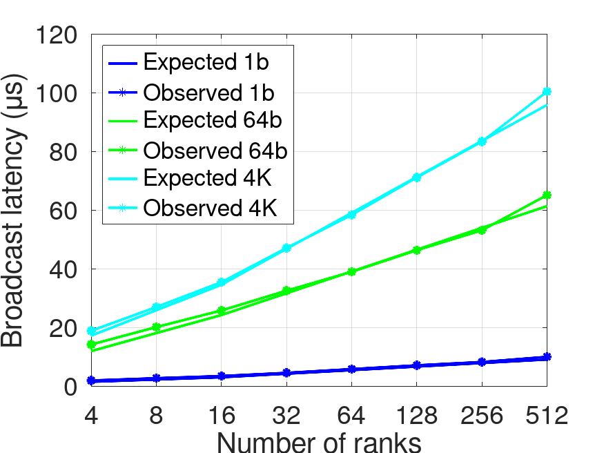
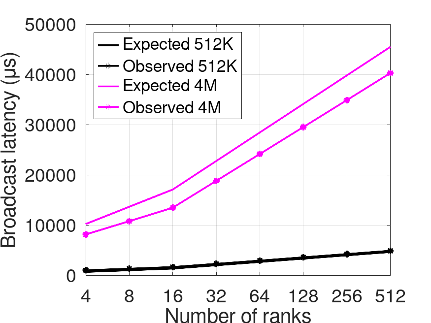
The main use of the expected broadcast latency expressed through Equation 1 is to assess how broadcast latency scales for an increasing number of participating processes. In the ideal case, expected and observed broadcast latency values should exhibit insignificant deviations. If instead, observed latency is larger than the expected and the gap grows with the number of participating processes, then, broadcast latency does not scale as expected. Such an unexpected increase would be a sign of performance inefficiency involving several aspects of the corresponding platform, including, the MPI library itself, the hardware blocks of the network interface and the exanet interconnect.
Figures 18(a), 18(b) present expected and actual broadcast latency for a different number of participating ranks and indicative message sizes. Regarding the small messages in Figure 18(a), the expected latency provided by Equation 1 is quite close to the observed one. For the case of e.g. 1 byte, the most notable deviation corresponds to the case of ranks where the actual broadcast latency is underestimated by approximately . However, for small messages, one way latency values can be as low as ns, constituting broadcast measurements more sensitive to phenomena like system noise and late arrivals. System noise (due to OS or running daemons) can have a significant effect on performance, especially for collectives, and can introduce variance in the performance observed (1592958, ; 10.1007/11602569_31, ; Jones03impactsof, ). Let us note that osu_bcast microbenchmark performs a quite fine grain timing by acquiring one timestamp before and one after each MPI_Bcast execution. Moreover, a barrier is used after each broadcast call. Disabling the barrier invocation and averaging latency over all iterations, results in an average broadcast latency of s. The corresponding underestimation of the actual broadcast latency becomes approximately , instead of . In Figure 18(a) we also see that as the number of ranks grows, the expected latency quite closely matches the observed one. The corresponding underestimation is for the case of ranks.
Another interesting observation regards the case of messages. For scenarios with ranks only, the expected latency is lower than the actual one. Apart from system noise and barrier effects, there is an additional reason that explains this gap. For messages that are larger than bytes, the actual data mover used is the RDMA engine (instead of the packetizer). When multiple ranks in the same MPSoC issue concurrent RDMA transfers, they share its bandwidth. This effect though is not captured by osu_one_way_lat which measures one way latency with a single pair of active processes per MPSoC. Accurately capturing the drop in throughput due to bandwidth sharing is not that easy depends on the overlap in time exhibited by the two concurrent transfers. It is also worth mentioning that, in the case of messages and or more ranks, the absolute value of the deviation is less than . A pattern similar to that of messages applies for the larger messages depicted in Figure 18(b). Equation 1 underestimates the observed latency by and for the case of ranks and messages of and respectively. For larger messages though, the effect of RDMA bandwidth sharing is expected to be more prominent. It is also worth mentioning that the deviation between the expected and actual broadcast latency is less than for most of the scenarios explored and plotted in Figure 18(b) (especially for large numbers of participating processes). Overall, broadcast latency seems to increase in a predictable manner as the number of participating ranks increases.
6.1.5. Accelerated allreduce collective
In this section, we report on the evaluation based on MPI microbenchmarks. The main target of this process is to assess the benefit of the allreduce accelerator which is part of the Network Interface (more details in Section 4.7). For that reason, we derive osu_allreduce latencies for two different ExaNet-MPI configurations: in the first one, the Allreduce collective is handled in software and is implemented through a recursive doubling algorithm, while in the second configuration, Allreduce is handled by our custom accelerator block. We explore four different experimental setups, involving , , and ranks. The main reason for having a maximum tested number of ranks , is that the current version of the allreduce accelerator can be used by at most one rank per MPSoC, thus one MPI process is spawned in each MPSoC. The message sizes involved in the allreduce operation range from bytes to KBytes. For messages larger than KBytes, the accelerator offers no benefit. The reason is that its current version divides messages in blocks of bytes, since it is also the maximum packet size that can traverse the ExaNet interconnect. The Allreduce Accelerator is triggered once for each block of bytes, which implies increased overhead for larger messages.
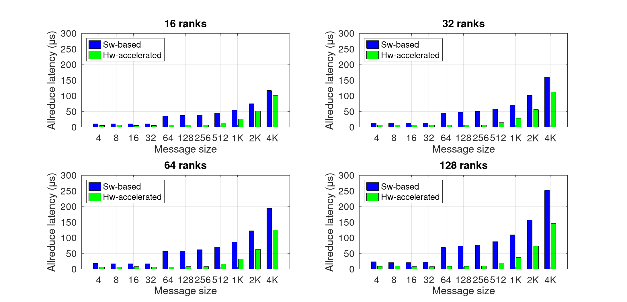
In Figure 19, we plot the compared osu_allreduce latency for the two configurations of ExaNet-MPI. In all setups presented, the accelerator achieves lower Allreduce latency than the software-based implementation. This drop is more profound for messages larger than bytes, where the software-based allreduce will use the RDMA engine as the data mover. Recall that RDMA offers increased throughput but incurs higher latency, when compared to the packetizer. Another interesting observation is the increased latency when the message size doubles. For the case of ranks and a message of bytes for example, the accelerator achieves an Allreduce latency of s. The corresponding values for and byte messages are and s, respectively. This effect of doubled latency is expected though, since as mentioned the logic of the accelerator is triggered once for each block of bytes. Let us note that, the maximum achieved improvement in Allreduce latency reaches , , , and for the four rank setups depicted in Figure 19. Finally, we note that, the accelerated Allreduce collective seems to scale better when the number of participating ranks increases. For the case of -bytes messages, the average osu_allreduce latency is respectively s for ranks and s for ranks, when using hardware acceleration. The corresponding values for the software-based implementation are and s, respectively. While the latency of the hardware-accelerated solution is almost stable, the latency of the software implementation almost doubles.
6.2. Full MPI application results
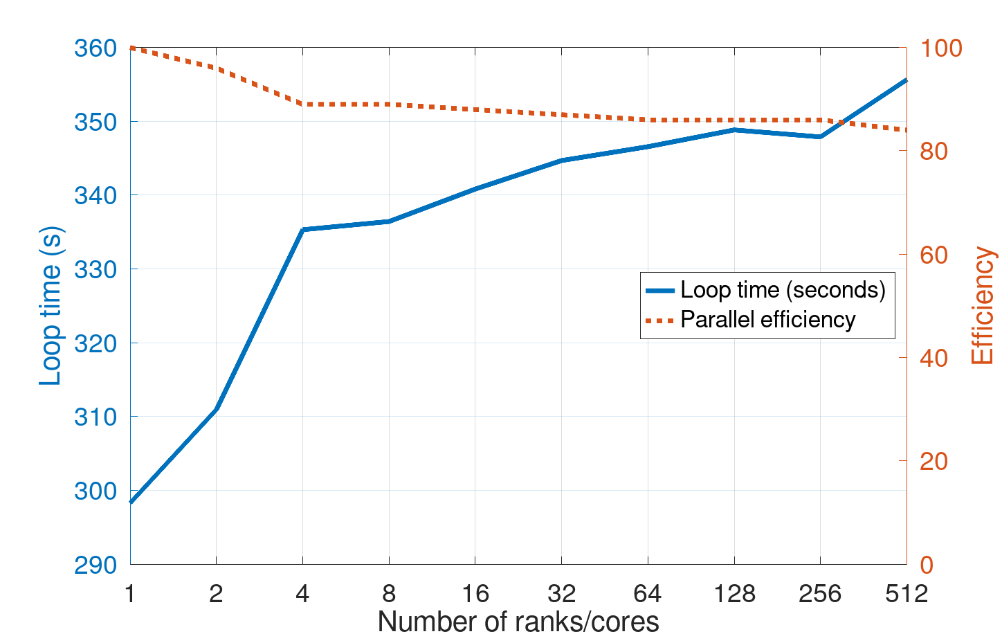
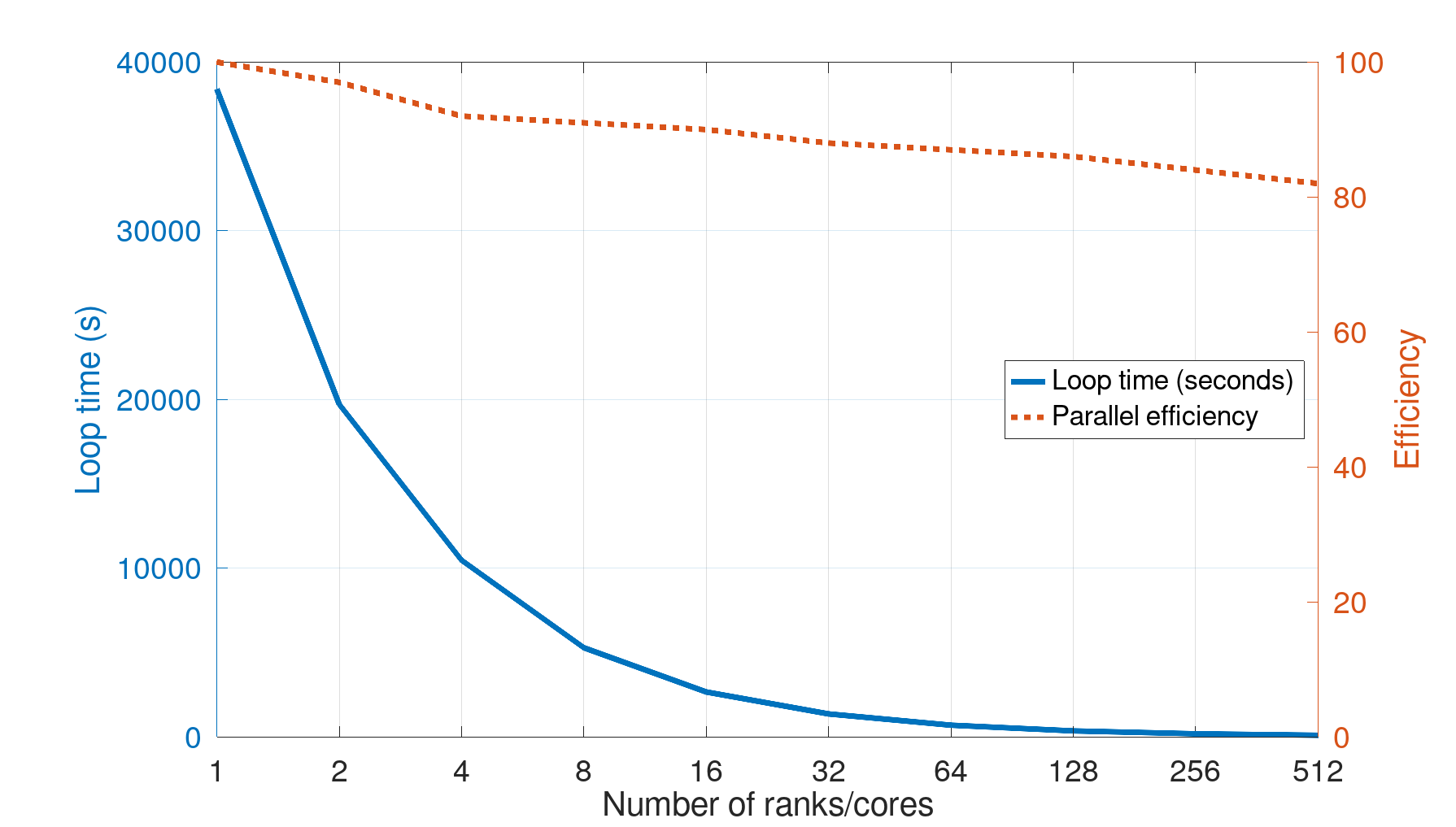
In this section, we evaluate the ExaNet interconnect running full MPI applications. The reported performance of an MPI application is the average performance of executions. The ExaNet-MPI runtime does not use the Allreduce accelerator described in Section 4.7. For all applications, we perform both weak- and strong-scaling tests. Apart from the actual performance achieved, we also calculate weak () and strong scaling efficiency () through the following equation: . In that equation, denotes the number of processes, assuming that each process runs on a separate core. is the speedup achieved when employing processes instead of a single one. To be more precise, for the benchmarks where performance is evaluated through completion time, speedup for the weak scaling tests is estimated through . In that equation, and denote the completion time for the case of a single and processes respectively. For the strong scaling tests, the corresponding speedup is .
We first evaluate the platform by running the rhodopsin protein benchmark of the Large-scale Atomic/Molecular Massively Parallel Simulator (LAMMPS) (LAMMPS, ), where we perform weak and strong scaling analysis. In Figure 20(a), a weak scaling analysis is performed executing in parallel to processes. Following the suggested configurations provided in (lammpsuserguide, ), timesteps are performed on a single core for a simulation of atoms. The simulation size when processes are executed in parallel is atoms. This figure presents the performance of LAMMPS depending on the number of cores used. The corresponding parallel efficiency –which measures how well an application leverages additional cores– is also shown. The left y-axis (loop time) in the figure depicts the total simulation time. We run one MPI rank on each CPU core. As this figure shows, the efficiency never drops below showing that, the application can scale well on many cores. However, there is a notable drop in the parallel efficiency when we have more than four MPI ranks. In particular, the parallel efficiency is and for two and four ranks, respectively. The main reason for this drop is that, the MPSoC includes four CPU cores. Thus, when all four cores are used, the contention to the main memory increases and the memory channel becomes the bottleneck. This is due to architectural limitations of the ZU9EG MPSoC, which supports a single memory channel to the main memory.
Figure 20(b) presents the results from the strong scaling analysis. As this figure shows, the LAMMPS rhodopsin protein benchmark can still scale well as system resources increase. Efficiency is above for all the system configurations. However, efficiency exhibits a notable drop as resources are added. This is a common case when running similar tests on similar size machines, as shown in (lammpsuserguide, ). Through a custom profiler, we derive the share of overall running time spent in communication. For the strong scaling test, average communication ratio is for the case of a single MPI rank and for the case of ranks.
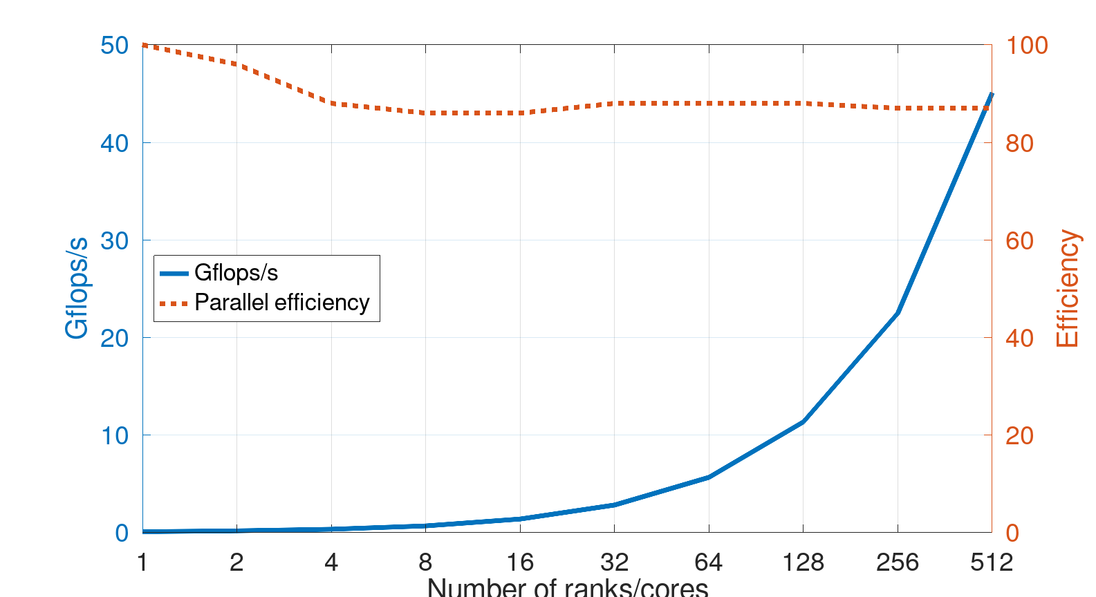
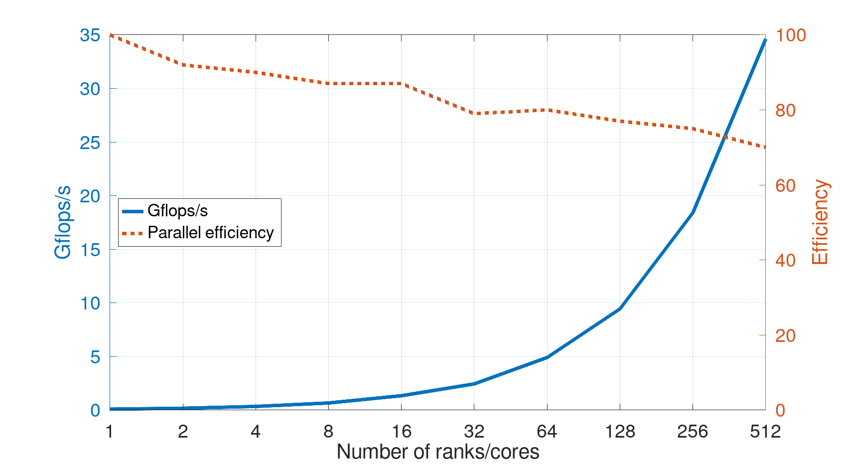
We next use the HPCG benchmark and perform both weak and strong scaling tests. For the strong scaling tests, the local problem size is set to the maximum problem size that fits in the memory of a single MPSoC for the case of a single run (nx=, ny=, nz=). For each different number of participating processes, we perform 15 different HPCG runs with duration for each run fixed to minutes (hpcgsite, ). The results depicted in Figure 21 comprise average GFLOPS over different executions. As Figure 21(b) shows, efficiency in the strong scaling test becomes , when using two instead of one core, and is for the case of ranks. Two indicative executions of HPCG, with two and MPI processes, reveal that the amount of time spent in communication is and , respectively. As far as the weak scaling test in Figure 21(a) is concerned, local problem size is set to nx=, ny=, nz= for the case of a single process. For the runs with participating processes, the global problem size becomes nx=, ny=, nz=. For the case of a single MPI rank, memory occupancy reaches approximately GBy. Efficiency is larger or equal than for all the weak scaling tests presented in Figure 21(a).
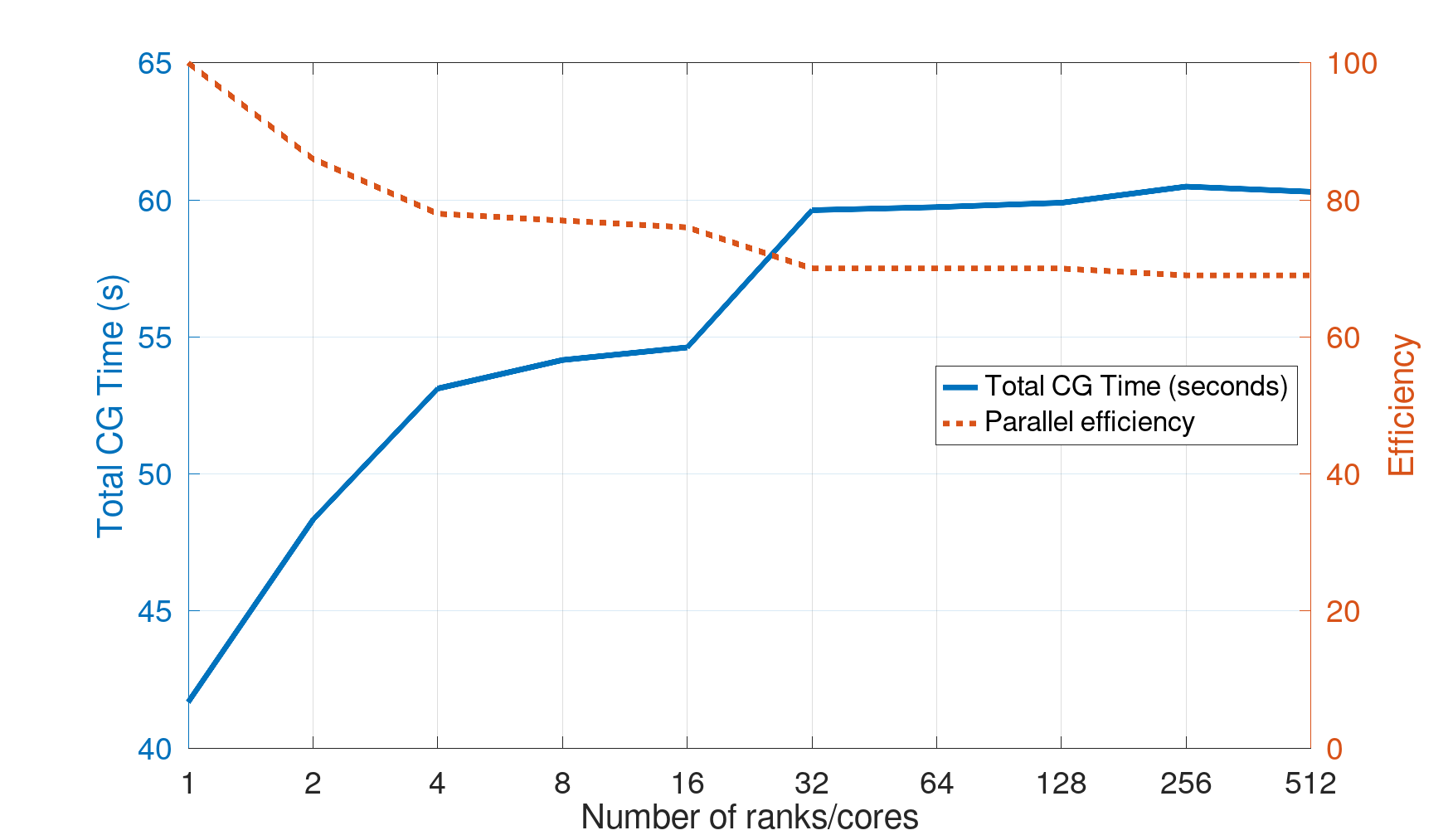
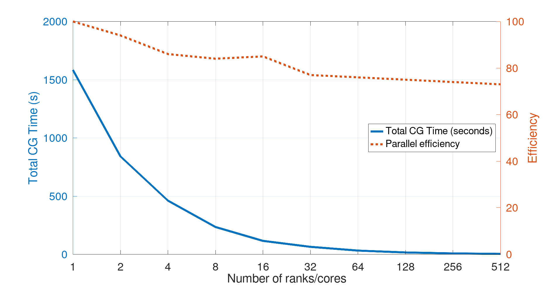
The final benchmark used to evaluate our platform is the (miniFE) miniapp from the Mantevo project (minifetechreport, ). For the strong scaling test, we fix the problem size to and the number of participating processes varies from a single one up to (i.e., full occupancy of the HPC prototype). For the weak scaling, we modify the miniFE source code to perform iterations. The main reason is that for a problem size of iterations and ranks, or more, final solution is not verified. For the case of ranks, the miniFE global problem size becomes .
Each one of Figures 22(a)-22(b) depicts both average miniFE performance and the corresponding parallel efficiency for the different setups applied. Performance is captured through the total Conjugate Gradient resolution time (reported as Total CG Time) and is the average of different runs. For the strong scaling test, efficiency is as high as when the number of processes is increased to . The corresponding value is for the weak scaling test. It should also be noted that, compared to the other benchmarks, miniFE spends a quite higher fraction of time spent in communication. In the weak scaling test and the case of four processes for example, the amount of conjugate gradient resolution time spent in communication is approximately . As the number of participating processes increases, so does the communication time reaching a ratio corresponding to for the case of processes. Even in this case though, efficiency is almost .
As an overview, Table 3 presents minimum and maximum values of parallel efficiency for the three MPI applications considered. These values correspond to configurations with 512 and two processes respectively.
| Weak scaling | Strong scaling | |||
|---|---|---|---|---|
| Processes | 2 | 512 | 2 | 512 |
| Lammps | 96% | 69% | 97% | 82% |
| HPCG | 96% | 87% | 92% | 70% |
| MiniFE | 86% | 69% | 94% | 72% |
7. Hardware Acceleration
The high-speed AXI-based memory interfaces between the FPGA and the Processing System (PS) in the Xilinx ZU9EG MPSoC enable the deployment of hardware accelerators tightly coupled with the processor. To showcase the capabilities of the ExaNeSt prototype, High-Level Synthesis (HLS) was used to develop a Matrix Multiplication accelerator, as it is a very common kernel in HPC and AI applications – for instance GEMM in BLAS Level-3 routines and also in Convolutional Neural Networks. In contrast to Section 6 that provided results for the complete ExaNeSt platform, this section focuses on a single QFDB, where all the FPGA resources are used by the accelerator.
Xilinx’s Vivado HLS was used to develop a highly optimized matrix multiplication kernel tile using the directive-oriented style of HLS. This kernel tile is parameterizable with different sizes, in order to experiment with implementations that have different area vs. performance trade-offs. The kernel tile operates on single-precision floating point elements (FP32) and is tuned considering the finite reconfigurable resources (LUTs, Flip-Flops, DSPs) and the internal memory (BRAM) size limitations. Moreover, its design uses efficiently the provided AXI memory bandwidth.
The basic matrix multiplication algorithm is shown below:
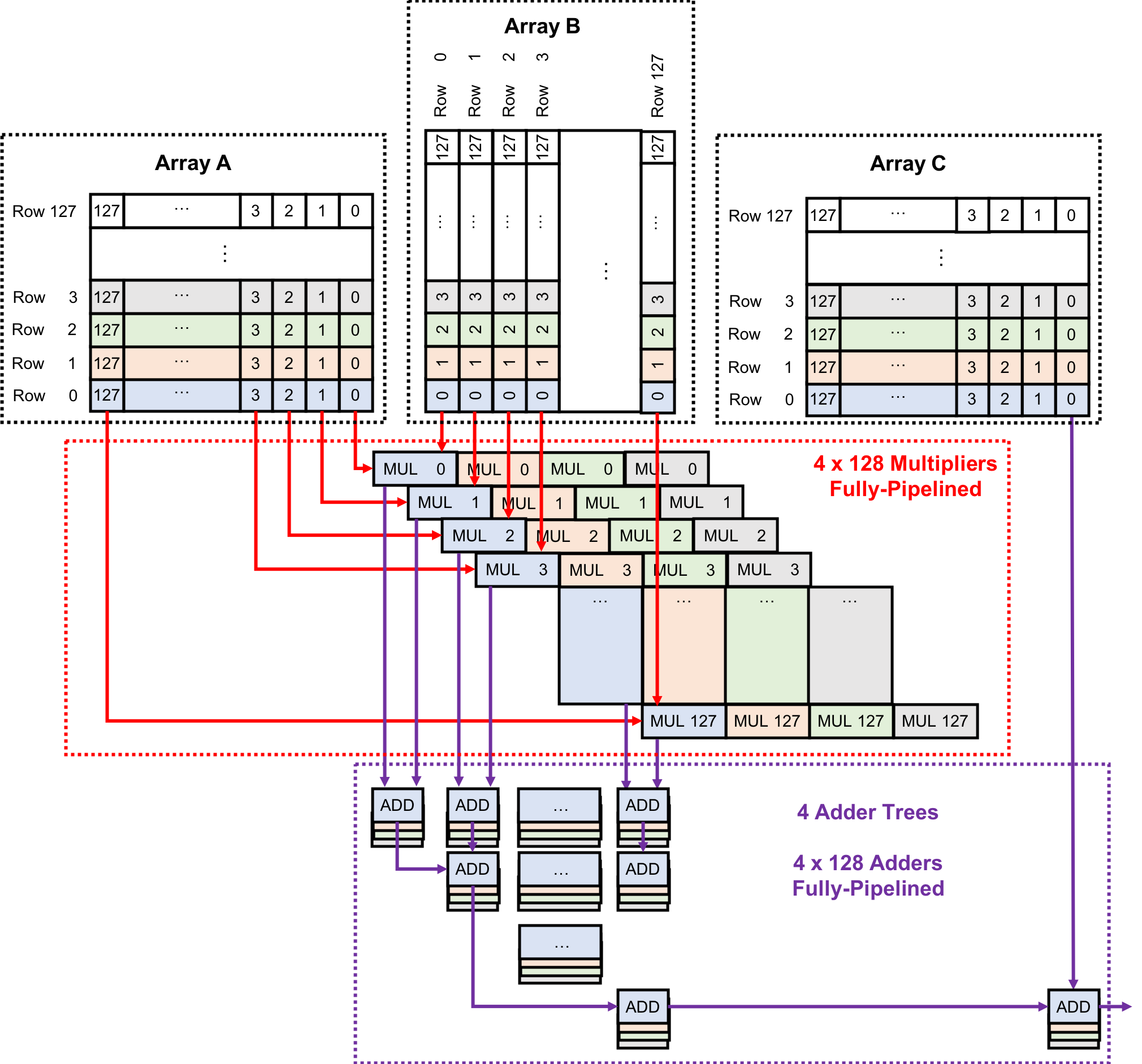
Given the finite resources of the FPGA and the need to accelerate matrix multiplication of very large arrays that do not fit in internal memory (BRAM), a tiled approach was followed, and the optimized kernel was applied over the corresponding tiles of the original arrays. Based on the study of the associated area-speed trade-offs, a tile size of , as depicted in Figure 23, operating at 300 MHz was selected. The kernel tile implementation unrolls the loop completely, performing 128 FP32 multiplications and 128 FP32 additions per cycle (fully-pipelined), which is similar to a vector unit operating on 4096 bits. Moreover, the loop is partially unrolled by a factor of 4, which is similar to having 4 vector units of 4096 bits. In total, the kernel tile performs 512 FP32 multiplications and 512 FP32 additions per cycle (fully-pipelined). Once the appropriate elements of the arrays are stored in on-chip accelerator memory (BRAMs), the tile execution lasts 4200 clock cycles. Three AXI HP ports (one per array) are utilized to load data into the local BRAMs, in order to continuously feed the kernel with data and match the required bandwidth. By performing a series of performance optimizations on the memory interfaces and load/unload techniques, each FPGA managed to achieve 275 FP32 GFLOPS and offload a matrix multiplication application from Linux. With all four FPGAs, a single QFDB can perform and sustain more than 1 FP32 TFLOP/s.
The matrix multiplication FP32 kernel tile of operates at 300 MHz, and requires 153K LUTs, 300K Flip-Flops, 2057 DSP macros and 416 BRAMs. The resource utilization of each FPGA device implementing our kernel tile is 56% of LUTs, 55% of Flip-Flops, 46% of BRAMs and 82% of DSPs. Moreover, power consumption of the accelerator was measured using the power sensors residing on the QFDB. Based on the readings of these sensors, encouraging power efficiency results were gathered. These measurements show that the dynamic power consumption of the accelerator is 16.2 Watts, which yields 17 FP32 GFLOPS per Watt.
8. Conclusion
We presented the ExaNeSt FPGA-based prototype, which interconnects Xilinx Ultrascale+ MPSoC FPGAs using 10 to 16 Gb/s links in a 3-dimensional Torus topology. Each FPGA contains four ARM Cortex-A53 cores and reconfigurable logic, in which the firmware for the ExaNet interconnect is implemented. This interconnect provides user-level access to hundreds of RDMA channels and offers a fast, sub-microsecond engine for small transfers, and a throughput-optimized reliable-RDMA engine for MPI rendez-vous. The RDMA engine uses ARM’s System-MMU for address translation, and segments transfers into blocks. We presented extensive evaluation results, using HPC codes running on up to 512 ARM Cortex-A53 cores/ranks.
To evaluate the ExaNeSt interconnect, we run microbenchmarks and real HPC codes on a 512-core system. The raw bandwidth inside the FPGA is 19.2 Gb/s, while the MPI bandwidth inside one FPGA or between FPGAs in the same QFDB is 13 Gb/s, dropping to 6.4Gb/s outside the QFDB. Best-case latency between adjacent FPGAs is 470 ns, split between hardware path and user-level access library. For the weak ARM Cortex-A53 core, the minimal MPI runtime adds almost 800 ns, and the RDMA latency for the same message size is 5 µs. MPI microbenchmarks reveal that broadcast latency scales as expected. Moreover, application level results show that efficiency in all tests exceeds 69%. In spite of the inefficiencies introduced by the Cortex-A53 processors, the minimal MPI port achieves good scaling efficiency by leveraging the user-level primitives.
We also designed a network hardware accelerator for MPI Allreduce, and a matrix-multiplication accelerator that achieves 275 GFLOPS per MPSoC and an energy efficiency of 17 GFLOPS per Watt for FP32 precision. We implemented these in the FPGA logic, thus eliminating software overheads.
Overall, we consider the following to be the main contributions of the ExaNest prototype:
-
•
Multi-processor testbed with configurable hardware support for communication - The first platform to integrate 256 FPGAs and offering a multi-processor environment with configurable communication, as discussed in Section 3.
-
•
Dense node-level and system-level integration - At the node level, the ExaNest prototype integrates 4 FPGAs (ZU9EG MPSoCs), 4 DRAM modules (DDR4 SODIMMs), and an M.2 Solid-State Disk (SSD) on a 120mm x 130mm x 21mm compute node. At the system level, the ExaNest prototype integrates four such compute nodes into a liquid-cooled thin (47mm thickness) blade. for optimal thermal management and high-density computing.
-
•
Low-cost, low-latency Network Interface offering virtualization and fast completion notifications, tightly coupled with the ARMv8 processing cores, as discussed in Section 4.
-
•
A custom MPI runtime leveraging Network Interface’s capabilities for user-level zero-copy transfers, and providing efficient communication for a variety of applications as discussed in Section 6.
9. Ongoing Work
We have been utilizing the ExaNeSt prototype as a platform to develop, test, and enhance High-Performance Computing (HPC) interconnect technologies. Within the RED-SEA EuroHPC project, we are also developing caRVnet, the next generation of ExaNet. caRVnet quadruples the data lane width (512 vs 128 bit) in the FPGA, and runs at 200MHz, thus achieving 100 Gb/s line rate. We are also implementing a testbed with a spine-leaf topology, consisting of an ExaNeSt mezzanine (4 QFDBs with 16 MPSoCs) and four central crossbars at the spine. Additionally, we are developing real-time monitoring and traffic generation tools that are capable of replaying arbitrary scenarios mixing victim and background flows. In other configurations, we are replaying background traffic to generate congestive episodes in parallel with MPI applications, and analyze the performance degradation under different congestion management schemes. We are further improving the network interface by incorporating a new hardware segmentation engine that reduces RDMA latency to below 0.5s and significantly enhances the transfer rate for small messages. Finally, we are integrating the network interface with RISC-V processors using the CHI protocol and we are connecting it with BXI network switches (bxi, ).
Acknowledgements
The Prototype Rack described in this paper was designed, built, and tested within the ExaNeSt (FET-HPC) project (2015-2019), funded by the European Union’s Horizon 2020 research and innovation programme under grant agreement No 671553. Its firmware and runtimes were improved within the EuroEXA project (2017-2021), similarly funded under grant agreement No 754337. It is now being used in large-scale congestion management experiments in the RED-SEA EuroHPC project (2021-2024), under grant agreement No 955776.
We wish to thank all the ExaNeSt partners for their help throughout the project: Iceotope Technologies Ltd. (UK), Istituto Nazionale di Fisica Nucleare - INFN (IT), the University of Manchester (UK), EnginSoft Spa (IT), Istituto Nazionale di Astrofisica - INAF (IT), Exact Lab Srl (IT), Universitat Politecnica de Valencia (ES), MonetDB Solutions B.V. (NL), Virtual Open Systems Sarl (FR), Allinea Software Ltd. - now part of ARM (UK), and Fraunhofer (DE).
We also wish to thank the members of our CARV Laboratory at FORTH-ICS who contributed to other related aspects of the project: Antonis Psathakis, Babis Aronis, Panagiotis Peristerakis, Antonis Psistakis, Ioannis Vardas, Polyvios Pratikakis, Leandros Tzanakis, and Kyriakos Paraskevas.
References
- (1) N. Adiga, G. Almasi, G. Almasi, Y. Aridor, R. Barik, D. Beece, R. Bellofatto, G. Bhanot, R. Bickford, M. Blumrich, A. Bright, J. Brunheroto, C. Cascaval, J. Castanos, W. Chan, L. Ceze, P. Coteus, S. Chatterjee, D. Chen, G. Chiu, T. Cipolla, P. Crumley, K. Desai, A. Deutsch, T. Domany, M. Dombrowa, W. Donath, M. Eleftheriou, C. Erway, J. Esch, B. Fitch, J. Gagliano, A. Gara, R. Garg, R. Germain, M. Giampapa, B. Gopalsamy, J. Gunnels, M. Gupta, F. Gustavson, S. Hall, R. Haring, D. Heidel, P. Heidelberger, L. Herger, D. Hoenicke, R. Jackson, T. Jamal-Eddine, G. Kopcsay, E. Krevat, M. Kurhekar, A. Lanzetta, D. Lieber, L. Liu, M. Lu, M. Mendell, A. Misra, Y. Moatti, L. Mok, J. Moreira, B. Nathanson, M. Newton, M. Ohmacht, A. Oliner, V. Pandit, R. Pudota, R. Rand, R. Regan, B. Rubin, A. Ruehli, S. Rus, R. Sahoo, A. Sanomiya, E. Schenfeld, M. Sharma, E. Shmueli, S. Singh, P. Song, V. Srinivasan, B. Steinmacher-Burow, K. Strauss, C. Surovic, R. Swetz, T. Takken, R. Tremaine, M. Tsao, A. Umamaheshwaran, P. Verma, P. Vranas, T. Ward, M. Wazlowski, W. Barrett, C. Engel, B. Drehmel, B. Hilgart, D. Hill, F. Kasemkhani, D. Krolak, C. Li, T. Liebsch, J. Marcella, A. Muff, A. Okomo, M. Rouse, A. Schram, M. Tubbs, G. Ulsh, C. Wait, J. Wittrup, M. Bae, K. Dockser, L. Kissel, M. Seager, J. Vetter, and K. Yates. An overview of the bluegene/l supercomputer. In SC ’02: Proceedings of the 2002 ACM/IEEE Conference on Supercomputing, pages 60–60, 2002.
- (2) I. Advanced Micro Devices. Alveo adaptable accelerator cards for data center workloads, 2022.
- (3) S. Agarwal, R. Garg, and N. K. Vishnoi. The impact of noise on the scaling of collectives: A theoretical approach. In D. A. Bader, M. Parashar, V. Sridhar, and V. K. Prasanna, editors, High Performance Computing – HiPC 2005, pages 280–289, Berlin, Heidelberg, 2005. Springer Berlin Heidelberg.
- (4) R. Ammendola, M. Guagnelli, G. Mazza, F. Palombi, R. Petronzio, D. Rossetti, A. Salamon, and P. Vicini. Apenet: a high speed, low latency 3d interconnect network. In cluster, page 481. Citeseer, 2004.
- (5) A. Armejach, B. Brank, J. Cortina, F. Dolique, T. Hayes, N. Ho, P.-A. Lagadec, R. Lemaire, G. López-Paradís, L. Marliac, M. Moretó, P. Marcuello, D. Pleiter, X. Tan, and S. Derradji. Mont-blanc 2020: Towards scalable and power efficient european hpc processors. In DATE, pages 136–141, 2021.
- (6) R. Baxter, S. Booth, M. Bull, G. Cawood, J. Perry, M. Parsons, A. Simpson, A. Trew, A. McCormick, G. Smart, R. Smart, A. Cantle, R. Chamberlain, and G. Genest. Maxwell - a 64 fpga supercomputer. In Second NASA/ESA Conference on Adaptive Hardware and Systems (AHS 2007), pages 287–294, 2007.
- (7) A. Biagioni and et al. Red-sea: Network solution for exascale architectures. In The 25th Euromicro Conference on Digital System Design (DSD) and SEAA (Software Engineering and Advanced Applications) Conference, volume Spain, Sept. 2022.
- (8) BittWare. Bittware fpga acceleration, 2019.
- (9) M. Blott. Reconfigurable future for hpc. In 2016 International Conference on High Performance Computing Simulation (HPCS), pages 130–131, July 2016.
- (10) B. Brech, J. Rubio, and M. Hollinger. Data engine for nosql - ibm power systems edition. White Paper, 2015.
- (11) F. Chaix, A. Ioannou, N. Kossifidis, N. Dimou, G. Ieronymakis, M. Marazakis, V. Papaefstathiou, V. Flouris, M. Ligerakis, G. Ailamakis, T. Vavouris, A. Damianakis, M. Katevenis, and I. Mavroidis. Implementation and impact of an ultra-compact multi-fpga board for large system prototyping. In 2019 IEEE/ACM International Workshop on Heterogeneous High-performance Reconfigurable Computing (H2RC), pages 34–41, 2019.
- (12) N. Chrysos, L. Chen, C. Kachris, and M. Katevenis. Discharging the network from its flow control headaches: Packet drops and hol blocking. IEEE/ACM Transactions on Networking, 24(1):15–28, 2015.
- (13) A. Cilardo. Htcomp: bringing reconfigurable hardware to future high-performance applications. IJHPCN, 12(1):74–83, 2018.
- (14) C. C. Corp. The convey hc-2 computer architectural overview (white paper). https://www.micron.com/-/media/documents/products/white-paper/wp_convey_hc2_architectual_overview.pdf, 2012.
- (15) P. Crozier, H. Thornquist, R. Numrich, A. Williams, H. Edwards, E. Keiter, M. Rajan, J. Willenbring, D. Doerfler, and M. Heroux. Improving performance via mini-applications. 01 2009.
- (16) B. Dally. Power, programmability, and granularity: The challenges of exascale computing. In 2011 IEEE International Parallel Distributed Processing Symposium, pages 878–878, 2011.
- (17) S. Derradji, T. Palfer-Sollier, J.-P. Panziera, A. Poudes, and F. W. Atos. The bxi interconnect architecture. In 2015 IEEE 23rd Annual Symposium on High-Performance Interconnects, pages 18–25, 2015.
- (18) Digilent Inc. FPGA, Microcontrollers and Instrumentation. http://www.digilent.com, 2019.
- (19) J. Dongarra, M. A. Heroux, and P. Luszczek. High-performance conjugate-gradient benchmark: A new metric for ranking high-performance computing systems. The International Journal of High Performance Computing Applications, 30(1):3–10, 2016.
- (20) F. A. Escobar, X. Chang, and C. Valderrama. Suitability analysis of fpgas for heterogeneous platforms in hpc. IEEE Transactions on Parallel and Distributed Systems, 27(2):600–612, Feb 2016.
- (21) A. P. et al. A reconfigurable fabric for accelerating large-scale datacenter services. In ACM/IEEE 41st International Symposium on Computer Architecture, ISCA 2014, Minneapolis, USA, June 14-18, pages 13–24, 2014.
- (22) A. P. et al. A reconfigurable fabric for accelerating large-scale datacenter services. Commun. ACM, 59(11):114–122, 2016.
- (23) J. O. et al. SDA: software-defined accelerator for large-scale DNN systems. In 2014 IEEE Hot Chips 26 Symposium (HCS), Cupertino, CA, USA, August 10-12, 2014, pages 1–23, 2014.
- (24) M. Y. et al. A performance evaluation of CUBE: one-dimensional 512 FPGA cluster. In Reconfigurable Computing: Architectures, Tools and Applications, 6th International Symposium, ARC 2010, Bangkok, Thailand, March 17-19, 2010. Proceedings, pages 372–381, 2010.
- (25) European Exascale System Interconnect and Storage - ExaNeSt. https://www.exanest.eu.
- (26) A. Fell, D. J. Mazure, T. C. Garcia, B. Perez, X. Teruel, P. Wilson, and J. D. Davis. The marenostrum experimental exascale platform (meep). Supercomputing Frontiers and Innovations, 8(1):62–81, Apr. 2021.
- (27) A. D. George, M. C. Herbordt, H. Lam, A. G. Lawande, J. Sheng, and C. Yang. Novo-g#: Large-scale reconfigurable computing with direct and programmable interconnects. In 2016 IEEE High Performance Extreme Computing Conference (HPEC), pages 1–7, 2016.
- (28) D. Giannopoulos, N. Chrysos, E. Mageiropoulos, G. Vardas, L. Tzanakis, and M. Katevenis. Accurate congestion control for rdma transfers. In 2018 Twelfth IEEE/ACM International Symposium on Networks-on-Chip (NOCS), pages 1–8, 2018.
- (29) D. Giannopoulos, N. Chrysos, E. Mageiropoulos, G. Vardas, L. Tzanakis, and M. Katevenis. Accurate congestion control for rdma transfers. In 2018 Twelfth IEEE/ACM International Symposium on Networks-on-Chip (NOCS), pages 1–8. IEEE, 2018.
- (30) S. GmbH. Sciengines hardware, high performance reconfigurable computing, 2019.
- (31) R. L. Graham, G. M. Shipman, B. W. Barrett, R. H. Castain, G. Bosilca, and A. Lumsdaine. Open mpi: A high-performance, heterogeneous mpi. In 2006 IEEE International Conference on Cluster Computing, pages 1–9, 2006.
- (32) W. Gropp, E. Lusk, N. Doss, and A. Skjellum. A high-performance, portable implementation of the mpi message passing interface standard. Parallel Computing, 22(6):789–828, 1996.
- (33) T. Hoefler, T. Schneider, and A. Lumsdaine. Accurately measuring collective operations at massive scale. In 2008 IEEE International Symposium on Parallel and Distributed Processing, pages 1–8, 2008.
- (34) HPCG Benchmark. https://hpcg-benchmark.org/index.html.
- (35) S. Hunold and A. Carpen-Amarie. Reproducible mpi benchmarking is still not as easy as you think. IEEE Transactions on Parallel and Distributed Systems, 27(12):3617–3630, 2016.
- (36) ICEOTOPE. Iceotope: Precision immersion cooling from the cloud to the edge, 2022.
- (37) A. D. Ioannou, K. Georgopoulos, P. Malakonakis, D. N. Pnevmatikatos, V. D. Papaefstathiou, I. Papaefstathiou, and I. Mavroidis. Unilogic: A novel architecture for highly parallel reconfigurable systems. volume 13, New York, NY, USA, Sept. 2020. Association for Computing Machinery.
- (38) T. R. Jones, L. B. Brenner, J. M. Fier, T. R. Jones, L. B. Brenner, and J. M. Fier. Impacts of operating systems on the scalability of parallel applications. Technical report, Lawrence Livermore National Laboratory, 2003.
- (39) N. D. Kallimanis, N. Chrysos, and M. Marazakis. A flexible & efficient shared memory abstraction with minimal hw assistance. May 2018.
- (40) N. D. Kallimanis, M. Marazakis, and N. Chrysos. Gsas: A fast shared memory abstraction with minimal hardware support. In EuroExaScale workshop - HiPEAC 2019, Valencia, Spain, January 2019.
- (41) G. Kalokerinos, V. Papaefstathiou, G. Nikiforos, S. Kavadias, M. Katevenis, D. Pnevmatikatos, and X. Yang. Fpga implementation of a configurable cache/scratchpad memory with virtualized user-level rdma capability. In 2009 International Symposium on Systems, Architectures, Modeling, and Simulation, pages 149–156, 2009.
- (42) M. Katevenis, N. Chrysos, M. Marazakis, I. Mavroidis, F. Chaix, N. Kallimanis, J. Navaridas, J. Goodacre, P. Vicini, A. Biagioni, P. S. Paolucci, A. Lonardo, E. Pastorelli, F. L. Cicero, R. Ammendola, P. Hopton, P. Coates, G. Taffoni, S. Cozzini, M. Kersten, Y. Zhang, J. Sahuquillo, S. Lechago, C. Pinto, B. Lietzow, D. Everett, and G. Perna. The exanest project: Interconnects, storage, and packaging for exascale systems. In 2016 Euromicro Conference on Digital System Design (DSD), pages 60–67, 2016.
- (43) M. G. Katevenis. Interprocessor communication seen as load-store instruction generalization. In In The Future of Computing, essays in memory of Stamatis Vassiliadis, K. Bertels ea (Eds.), Delft, The Netherlands. Citeseer, 2007.
- (44) R. Kobayashi, Y. Oobata, N. Fujita, Y. Yamaguchi, and T. Boku. Opencl-ready high speed fpga network for reconfigurable high performance computing. In Proceedings of the International Conference on High Performance Computing in Asia-Pacific Region, HPC Asia 2018, page 192–201, New York, NY, USA, 2018. Association for Computing Machinery.
- (45) G. Kornaros, D. Pnevmatikatos, P. Vatsolaki, G. Kalokerinos, C. Xanthaki, D. Mavroidis, D. Serpanos, and M. Katevenis. Implementation of atlas i: a single-chip atm switch with backpressure. In Proceedings of the IEEE Hot Interconnects 6 Symposium, pages 85–96. Citeseer, 1998.
- (46) Lammps user guide. https://docs.lammps.org/Speed_bench.html.
- (47) P. Lin, M. Heroux, R. Barrett, and A. Williams. Assessing a mini-application as a performance proxy for a finite element method engineering application. Concurrency and Computation: Practice and Experience, 08 2015.
- (48) Kexec. https://linux.die.net/man/8/kexec, 2021.
- (49) H. G. LLC. Xilinx / altera fpga boards, design services, & ip cores, 2019.
- (50) E. Markatos and M. Katevenis. User-level dma without operating system kernel modification. In Proceedings Third International Symposium on High-Performance Computer Architecture, pages 322–331, 1997.
- (51) Maxeler Technologies Inc. Maxeler Products. https://www.maxeler.com/products/, 2019.
- (52) Amazon.com Inc. Amazon EC2 F1 Instances. https://aws.amazon.com/ec2/instance-types/f1/, 2019.
- (53) Maxeler Technologies Inc. Dataflow Computing. https://www.maxeler.com/technology/dataflow-computing/, 2019.
- (54) A. Oleksiak, M. Kierzynka, W. Piatek, M. vor dem Berge, W. Christmann, S. Krupop, M. Porrmann, J. Hagemeyer, R. Griessl, M. Peykanu, L. Tigges, S. Rosinger, D. Schlitt, C. Pieper, U. Janssen, H. Rauchfuss, G. Agosta, A. Barenghi, C. Brandolese, W. Fornaciari, G. Pelosi, J. Pita Costa, M. Cecowski, R. Plestenjak, J. Cinkelj, L. Cudennec, T. Goubier, J.-M. Philippe, C. Adeniyi-Jones, J. Setoain, and L. Ceva. M2DC—A Novel Heterogeneous Hyperscale Microserver Platform, pages 109–128. Springer International Publishing, Cham, 2019.
- (55) OSU Micro-Benchmarks. http://mvapich.cse.ohio-state.edu/benchmarks/.
- (56) K. Paraskevas, N. Chrysos, V. Papaefstathiou, P. Xirouchakis, P. Peristerakis, M. Giannioudis, and M. Katevenis. Virtualized multi-channel rdmawith software-defined scheduling. Procedia Computer Science, 136:82–90, 2018.
- (57) O. Pell and V. Averbukh. Maximum performance computing with dataflow engines. Computing in Science and Engineering, 14(4):98–103, 2012.
- (58) O. Pell and O. Mencer. Surviving the end of frequency scaling with reconfigurable dataflow computing. SIGARCH Comput. Archit. News, 39(4):60–65, Dec. 2011.
- (59) F. Petrini, D. Kerbyson, and S. Pakin. The case of the missing supercomputer performance: Achieving optimal performance on the 8,192 processors of asci q. In SC ’03: Proceedings of the 2003 ACM/IEEE Conference on Supercomputing, pages 55–55, 2003.
- (60) C. Plessl. Bringing fpgas to hpc production systems and codes. In Fourth International Workshop on Heterogeneous High-performance Reconfigurable Computing, workshop at Supercomputing, 2018.
- (61) M. Ploumidis, N. D. Kallimanis, M. Asiminakis, N. Chrysos, P. Xirouchakis, M. Gianoudis, L. Tzanakis, N. Dimou, A. Psistakis, P. Peristerakis, G. Kalokairinos, V. Papaefstathiou, and M. Katevenis. Software and hardware co-design for low-power hpc platforms. page 88–100, Berlin, Heidelberg, 2019. Springer-Verlag.
- (62) A. Psistakis, N. Chrysos, F. Chaix, M. Asiminakis, M. Gianioudis, P. Xirouchakis, V. Papaefstathiou, and M. Katevenis. Optimized page fault handling during rdma. IEEE Transactions on Parallel and Distributed Systems, pages 1–1, 2022.
- (63) A. Psistakis, N. Chrysos, F. Chaix, M. Asiminakis, M. Giannioudis, P. Xirouchakis, V. Papaefstathiou, and M. Katevenis. Part: Pinning avoidance in rdma technologies. In 2020 14th IEEE/ACM International Symposium on Networks-on-Chip (NOCS), pages 1–8. IEEE, 2020.
- (64) A. SE. Bullsequana x supercomputers - atos, 2022.
- (65) C. B. Stunkel, R. L. Graham, G. Shainer, M. Kagan, S. S. Sharkawi, B. Rosenburg, and G. A. Chochia. The high-speed networks of the summit and sierra supercomputers. IBM Journal of Research and Development, 64(3/4):3:1–3:10, 2020.
- (66) G. Taffoni, L. Tornatore, D. Goz, A. Ragagnin, S. Bertocco, I. Coretti, M. Marazakis, F. Chaix, M. Plumidis, M. Katevenis, R. Panchieri, and G. Perna. Towards exascale: Measuring the energy footprint of astrophysics hpc simulations. In 2019 15th International Conference on eScience (eScience), pages 403–412, 2019.
- (67) A. P. Thompson, H. M. Aktulga, R. Berger, D. S. Bolintineanu, W. M. Brown, P. S. Crozier, P. J. in ’t Veld, A. Kohlmeyer, S. G. Moore, T. D. Nguyen, R. Shan, M. J. Stevens, J. Tranchida, C. Trott, and S. J. Plimpton. LAMMPS - a flexible simulation tool for particle-based materials modeling at the atomic, meso, and continuum scales. Comp. Phys. Comm., 271:108171, 2022.
- (68) Zynq ultrascale+ device technical reference manual, 2018.
- (69) A. Xilinx. Heterogeneous accelerated compute clusters, 2016.
- (70) Integrated Logic Analyzer v6.2. https://docs.xilinx.com/v/u/en-US/pg172-ila.