Intrinsic ferroelectric switching in two dimensions
Abstract
Two-dimensional (2D) ferroelectric semiconductors with electrically addressable polarization present opportunities for integrating ferroelectrics into high-density ultrathin nanoelectronics. However, efforts to improve critical characteristics such as switching speed and endurance of 2D ferroelectric-based devices have been hampered by the limited microscopic understanding of ferroelectric switching in 2D. Taking 2D -In2Se3 with out-of-plane polarization () as a model, we employ deep-learning-assisted large-scale molecular dynamics (MD) simulations to analyze the switching processes of 2D domains and 1D domain walls, revealing mechanisms fundamentally different from those of bulk ferroelectrics. We discover that a single domain is unswitchable by an out-of-plane electric field due to forbidden splitting of Wyckoff orbits. This “splitting restriction principle” also explains the robust presented in sliding ferroelectricity and moiré ferroelectricity. Counterintuitively, 1D domain walls are easily moved by in-plane fields despite lacking in-plane effective polarization. The field-driven 1D walls exhibit unusual avalanche dynamics characterized by abrupt, intermittent moving patterns. The propagating velocity at various temperatures, field orientations, and strengths can be statistically described with a single creep equation, featuring a dynamical exponent of 2 that is distinct from all known values for elastic interfaces moving in disordered media. We demonstrate a tunable onset field for the intrinsic creep-depinning transition, suggesting a simple route for on-demand configuration of switching speed.
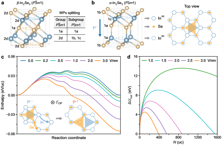
The depolarizaiton field that arises due to the imperfect screening of polarization bound charges on surfaces is inversely proportional to the thickness of the film [1]. The suppressed polarization along the direction of reduced dimensionality has been a main obstacle for the miniaturization of ferroelectric-based devices. Among the few synthesized 2D ferroelectrics, -In2Se3 has garnered considerable attention, partly because of its advantageous out-of-plane polarization [2, 3, 4]. This characteristic allows for full utilization of the atomic thickness, thereby opening avenues for the development of ultrathin nanoelectronics [5]. In addition to forming the phase, In2Se3 can crystallize into the phase with in-plane polarization () and the paraelectric phase (Fig. 1a) [6, 7, 8, 9]. Leveraging both polymorphism and ferroelectricity together establishes a versatile platform for unlocking new functionalities [10]. Several device prototypes, including ferroelectric channel transistor [11] and synaptic ferroelectric semiconductor junction [12], have been fabricated using quasi-2D In2Se3 films with a thickness of tens of nanometers, and some of these devices have shown high carrier mobility, decent retention time, and stable cycling endurance. Recent experiments have shown that van der Waals (vdW) stacked bilayers of nonferroelectric monolayers can be engineered into ferroelectrics through sliding and twisting [13, 14, 15, 16, 17], thus substantially expanding the family of 2D ferroelectrics possessing . Much like their bulk counterparts, the functional attributes of 2D ferroelectrics depend critically on the polarization response to external stimuli. The question remains whether various switching models developed for bulk ferroelectrics can be directly applied to reduced dimensions [18]. To improve the performance of 2D ferroelectric-based devices, an in-depth, atomic-level understanding of the switching mechanisms in 2D, a largely unexplored field, is crucial.
Monolayer -In2Se3 in the space group of consists of five atomic planes in the sequence of Se-In-Se-In-Se with each layer containing only one type of atom arranged in a triangular lattice (see Fig. 1b). Despite intensive research, the specifics of ferroelectricity in 2D -In2Se3 remain unclear. The structural origin of in monolayer -In2Se3 is the shift of the central Se layer along the -axis, breaking the out-of-plane inversion symmetry. However, the mechanism protecting against the depolarization effect is elusive. Moreover, first-principles density functional theory (DFT) calculations have predicted a rather low switching barrier of 66 meV per unit cell (uc) in monolayer -In2Se3 [19], yet the observed out-of-plane switching field is 1 V/nm (10 MV/cm) [4], several orders of magnitude higher than that for PbTiO3-based perovskite ferroelectrics (10 kV/cm) [20] with higher switching barriers. Furthermore, it has been commonly cited that -In2Se3 exhibits [6, 7], which directly contradicts Neumann’s principle since the C3v point group symmetry (out-of-plane three-fold rotational axis) of -In2Se3 strictly prohibits in-plane switchable polarization (also refereed to as effective polarization in modern theory of polarization [21, 22]). Despite this, multiple experimental studies have reported a switching-like behavior when an in-plane electric field () of 0.1 V/nm (much smaller than the out-of-plane switching field) is applied to -In2Se3 thin films [23]. At the most fundamental level, the controlled engineering of ferroelectric switching in 2D hinges on a quantitative characterization of the dynamics of 1D domain walls, which are nanoscale interfaces between differently polarized 2D domains. This endeavor has been particularly challenging due to the high temporal and spatial resolution required for both experimental and theoretical approaches, such that there is virtually no reported data on the velocity of 1D domain walls in 2D ferroelectrics. To summarize, currently there is no consensus, be it experimental or theoretical, on several key questions: (i) Why does monolayer -In2Se3, similar to vdW bilayers of stacking-engineered ferroelectricity, exhibit such a high out-of-plane switching field? (ii) How is it possible for to switch monolayer -In2Se3 despite the absence of in-plane effective polarization? (iii) What are the polarization switching dynamics involved in 2D domains and 1D walls?
We start with a symmetry argument to elucidate the resilience of against the depolarization field in 2D -In2Se3. The Landau theory, which explains symmetry-breaking structural phase transitions, presumes that such transitions result from the condensation of either a single or a group of collective degrees of freedom, conforming to a single irreducible representation (irrep) of the space group for the high-symmetry phase. We find that though paraelectric -In2Se3 (space group ) and ferroelectric -In2Se3 (space group ) conform to the group-subgroup relationship, the transition cannot be realized by a structural distortion associated with an irrep of : the atomic occupations in -In2Se3 and -In2Se3 prevent the required splitting of Wyckoff positions. Specifically, the In atoms occupy the 2d Wyckoff orbits in -In2Se3, while the two In atoms in -In2Se3 occupy 1a and 1c orbit, respectively, violating the allowed splitting rule of 2d1b/1c associated with (see Fig. 1a-b). This is fundamentally different from (proper) perovskite ferroelectrics, where a polar soft mode serves as the primary order parameter responsible for the paraelectric-ferroelectric phase transition [24]. Given that a depolarization field mainly suppresses the displacive distortion associated with the polar soft mode, we propose that in 2D -In2Se3 is protected by a principle we call “splitting restriction”, which refers to the forbidden splitting of Wyckoff orbits during the postulated phase transition. We highlight that the same mechanism also plays a crucial role in the stabilization of emerged in sliding and moiré ferroelectricity [25, 26, 27] (see detailed discussions about Bernal-stacked -BN in Sect. II of Supplementary Material). This is not entirely surprising, as -In2Se3 can be conceptualized as two laterally shifted InSe layers with intercalated Se atoms between them.
A deduction from the above symmetry analysis is that using to induce the reversal of could be difficult, due to the absence of a symmetry-adapted polar mode for efficient - coupling. This seems to contradict with the low switching barrier at zero field identified previously [19] as well as reproduced by our DFT-based nudged elastic band (NEB) calculations: the zero-field NEB barrier for the reversal of () is a mere 40 meV/uc (Fig. 1c), substantially lower than that of PbTiO3 (170 meV/uc). The low-barrier pathway involves concerted lateral shifts of entire layers of In and Se atoms (see inset of Fig. 1c), coupled to out-of-plane displacements that reverse . Intriguingly, despite bearing opposite charges, In and Se atoms must move in the same direction, thus being a process unlikely to be excited by . We further perform finite-field NEB calculations with varying magnitudes and confirm that is weakly dependent on field strength: even an intense of 3.0 V/nm (30 MV/cm) only moderately reduces the barrier to 25 meV/uc (Fig. 1c). Another important aspect is that corresponds to the barrier for a homogeneous switching mechanism during which all dipoles response synchronously to without nucleating oppositely polarized domains. This overlooks the energy costs involved in creating new interfaces that separate the newly formed nucleus and the surrounding domain.
The difficulty of reversing in an ideal 2D domain of -In2Se3 via is further corroborated by our large-scale MD simulations that employs a deep neural network-based force field trained with a large database of ab initio energies and atomic forces from 25,000 configurations of In2Se3 [28] (see Methods). We observe that a single-domain monolayer, constructed using an 18000-atom supercell, is immune to at 300 K (no switching detected within a simulation period of 3 nanoseconds), even when exposed to giant field strengths achievable in experimental setups. Only at an elevated temperature of 373 K is a nucleus formed with aligned with of 3.0 V/nm (see Figs. S4 of Supplementary Material). The change in the energy associated with the formation of a 2D nucleus containing unit cells can be approximated as [29]
| (1) |
where is the out-of-plane electric dipole moment per unit cell, is the (averaged) interface energy per unit-cell length of the boundary that separates the nucleus and the parent domain, and is a geometric factor depending on the nucleus shape. Using Å computed with DFT, eV and both extracted from MD (see Sect. III of Supplementary Material), Fig. 1d displays as a function of for various field strengths, revealing an exceptionally large size for the critical nucleus () and a high nucleation barrier, i.e., 870 for V/nm. The high 1D interfacial energy and the small magnitude of together make it energetically challenging to switch a 2D domain in monolayer -In2Se3. It is noted that the application of an in-plane field to a 2D domain will irreversibly drive the transition from to (with a lower symmetry in the space group of ) based on our MD simulations, consistent with experimental observations [8].
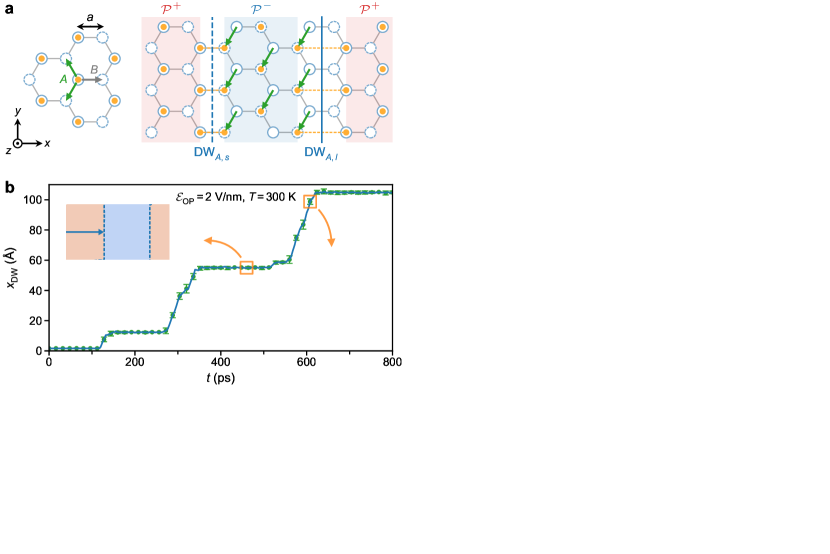
We will now demonstrate that pre-existing 1D domain walls are vital for experimentally observed -induced switching of . When viewed from the out-of-plane direction of a single domain, the two layers of In atoms resemble the hexagonal lattice of monolayer -BN with a (projected) bond length of , while middle-layer Se atoms occupy only one type of lattice site (Fig. 1b). There exist four variants of 180∘ domain walls, grouped into two pairs ( and ), that can be generated by an in-plane shift of a section of middle-layer Se atoms along the direction connecting In atoms by a distance of accompanied by an out-of-plane shift that flips the polarization direction. As illustrated in Fig. 2a, for each pair, there is a wide domain wall characterized by long Se-Se separations (e.g., DWA,l) and a narrow domain wall featuring short Se-Se bonds (e.g., DWA,s). We focus on type- walls for their greater thermodynamic stability compared to type- walls (see Sect. IV of Supplementary Material). Our MD simulations further show that only DWA,s is movable by ; DWA,l is immobile, consistent with its large barrier of 0.7 eV for domain wall motion, as predicted by DFT-based NEB calculations (see Table S2 in Supplementary Material). The temporal evolution of the averaged position of DWA,s driven by (Fig. 2b) unveils two characteristics that differ distinctly from 2D domain walls in bulk ferroelectrics [30, 29]. First, the motion of DWA,s exhibits avalanche dynamics, wherein this 1D interface moves abruptly and intermittently. Second, DWA,s acquires dynamic roughening: the initially flat wall becomes curved during its motion. The geometrical roughness, represented as error bars in Fig. 2b, is characterized by a global width of 1.8 Å.
By analyzing MD trajectories with a fine time resolution down to femtoseconds, we identify a “stone skipping”-like mechanism that explains the two intrinsic features of DWA,s motion emerged in the absence of defects (disorder pinning). As depicted in Fig. 2c, in the presence of , a line of Se atoms () closest to the boundary move towards the bottom of nearby Inup atoms (denoted as ). Simultaneously, a line of Indn atoms () shift towards those Se atoms of (denoted as ). This contrasts with the layer-by-layer switching mechanism pioneered by Miller and Weinreich for sideway motion of 2D domain walls [31]. Here, the movement of 1D DWA,s engages two lines of atoms and is somewhat reminiscent of the hypothesized “nuclei stacking” that is assumed to occur in a high-field-induced mobile rough wall (though rarely observed) [32]. Importantly, the transient interface, and , can jointly serve as a moving front (Fig. 2d). Specifically, subsequent processes of and , achieved via atomic movement pattern (Fig. 2d), effectively move the interface sideways by a distance of (Fig. 2f). At steps where movement does not take place, the line-by-line switching mechanism is recovered as the net outcome is (Fig. 2e). We propose that the interface is an “emergent” high-energy interface that only needs to overcome a small kinetic barrier to move (see the dashed line in Fig. 2g), analogous to a swiftly skipping stone on water. The probabilistic failure of movement could trigger the relaxation of to a flat, low-energy interface (DWA,s), the movement of which must overcome a large barrier (see the solid line in Fig. 2g). This stone-skipping-like mechanism intuitively explains the bursts of domain wall motions (attributable to the emergent fast-moving interface) separated by periods of inactivity (due to the reactivation of DWA,s). The dynamic roughening of DWA,s, manifested as a wavy moving font (see MD snapshots in Sect. V of Supplementary Material), is a consequence of the interplay between two distinct mechanisms of domain wall motion along an extended 1D interface. Across larger length scales, specific sections of the interface progress through the slower, line-by-line mechanism, while other segments advance more rapidly via the stone-skipping-like mechanism. This differential speed of movement along the interface’s length results in the curvature during its motion.
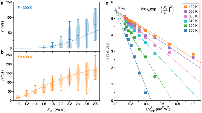
We use MD simulations to quantitatively estimate the velocity () of DWA,s over a wide range of temperatures () and . It is noted that the value of is calculated by measuring the distance that the wall traverses within a specific time frame, while also taking into account the periods of inactivity when the wall is stationary. Due to the inherent avalanche dynamics, the values of , obtained from multiple MD trajectories, exhibit a considerable fluctuation for a specific and , as shown by the violin plots at 300 K and 400 K (Fig. 3a-b). Remarkably, even in the absence of defects, we discover that the mean 1D domain wall velocity, , can be well described with a creep process as [33, 34]
| (2) |
where is the domain wall velocity under an infinite field, is the temperature-dependent activation field. Within a statistical description of domain wall motion as a critical phenomenon, that is, an elastic interface moving in random media, is the creep exponent that depends on the dimensionality of the interface and the universality class of the disorder landscape pinning the interface [25]. As depicted in Fig. 3c, the plots of versus curves yield linear relationships across a broad spectrum of field strengths (1.0–2.8 V/nm) and various temperatures (300–400 K). Notably, all linear fits converge at the same intercept that corresponds to 247 m/s. This serves as a strong evidence for an unusual creep exponent, , higher than the well-known value of for 1D magnetic domain walls in ultrathin magnetic films [25] as well as for 2D ferroelectric domain walls in typical perovskite ferroelectrics [35, 29]. We propose -driven creep motion of DWA,s in monolayer -In2Se3 probably belongs to an entirely new universality class. A higher value of creep exponent implies that this interface is more sensitive to changes in the magnitude of , especially at low driving forces, which is advantageous for fine-tuning domain wall mobility. Moreover, we observe the absence of an intrinsic creep–depinning transition, even at a colossal field strength of 2.8 V/nm (28 MV/cm), likely attributable to the small Born effect charges (0.49 for In and for Se) in the out-of-plane direction: the weak - coupling is insufficient to reduce the barrier of domain wall motion compared to thermal fluctuations, thus leading to persistent creep behavior of DWA,s.
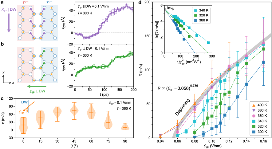
The movement of DWA,s driven by involves in-plane displacements of In and Se atoms near the boundary (Fig. 2c-f), hinting at a potential coupling between DWA,s and in-plane fields. Considering the symmetry, the presence of DWA,s locally disrupts the C3v point group symmetry, in turn generating local dipoles in DWA,s that could be coupled to . This is confirmed by our finite-field MD simulations, which demonstrate -driven DWA,s motion. Importantly, owing to the large in-plane Born effective charges of Se and In atoms, applying of 0.12 V/nm is sufficient to drive the movement of DWA,s within 100 ps at 300 K. This field strength is notably lower than what would be needed when is applied, and is comparable to the field strengths (0.2 V/nm) used in experiments [23] .
The -driven DWA,s motion is found to exhibit a pronounced field-orientation dependence. When is applied parallel to DWA,s (), this 1D interface shows an equal likelihood of moving either to the left or the right, corresponding microscopically to the equally probable hopping processes of Se atoms situated in proximity to DWA,s (Fig. 4a). This behavior is a manifestation of spontaneous symmetry breaking: while does not inherently favor any particular direction due to the lack of physical in-plane polarization, the wall opts for a specific direction, which is induced by thermal activation. The temporal progression of the domain wall position (Fig. 4a) clearly demonstrates that DWA,s retains the avalanche dynamics and oscillates back and forth in a stochastic manner in the case of . In comparison, when is applied perpendicular to DWA,s (), the wall moves deterministically, in the direction counter to that of the Se atom hopping (Fig. 4b). We map out as a function of the relative orientation () between (of 0.1 V/nm) and the wall at 360 K, showing a strong anisotropy with the maximum velocity peaking at (Fig. 4c). Such highly tunable domain wall mobility is beneficial for controlled design of polarization switching speed.
The - and -dependent mean velocity of DWA,s for =45∘ is displayed in Fig. 4d, indicating an intrinsic creep-depinning transition [29]. In particular, the velocity data at temperatures exceeding 340 K overlap when V/nm, a hallmark feature of depinning wherein the velocity becomes temperature independent. These velocity data can be fitted to
| (3) |
where is a velocity exponent and is the crossing field at zero Kelvin. The fitting yields , a value nearly identical to the reported velocity exponent of 0.72 for 90∘ domain walls in PbTiO3. This implies the existence of universal depinning dynamics for domain walls in 2D and 3D ferroelectrics. At temperatures of 340 K or lower, the velocity has a strong dependence on temperature and exhibits a nonlinear relationship with , suggesting a creep behavior. As presented in the inset of Fig. 4d, the velocity data in the creep region can be well described by equation (2) using the same parameters, m/s and , as derived from -driven DWA,s motions shown in Fig. 3c. The velocity data collected under both and affirm the robustness of an atypical creep exponent of 2, supporting the presence of a new universality class.
Our multiscale investigation that combines symmetry analysis, DFT, large-scale MD, and analytical modeling on the ferroelectric switching in 2D addresses the three aforementioned questions. First, the forbidden splitting of Wyckoff orbits for the transition from paraelectric -In2Se3 to ferroelectric -In2Se3 introduces a trade-off between the robustness of and the difficulty in switching it: the lack of a symmetry-adapted polar mode renders stable against the depolarization field but also makes - coupling rather inefficient. This splitting restriction principle, along with the resultant difficulty of -driven polarization reversal, is expected to be a prevalent characteristic across a wide spectrum of vdW bilayers exhibiting sliding ferroelectricity and morié ferroelectricity. The existence of domain walls, particularly DWA,s, is found to be essential for the ferroelectric switching driven by in 2D -In2Se3. The giant magnitude of (at the order of 1 V/nm) required for moving domain walls, as predicted by our MD simulations and corroborated by experiments [4], can be attributed to the weak - coupling. Second, despite the lack of switchable in single-domain 2D -In2Se3 caused by the out-of-plane three-fold rotational axis, the existence of DWA,s breaks this symmetry on a local level, allowing for a coupling between local dipoles of DWA,s and . Benefiting from the large in-plane Born effective charges and the unique mechanism of DWA,s motion involving in-plane atomic displacements, applying proves to be more efficient than using for inducing ferroelectric switching, resolving a longstanding inconsistency between experimental observations and theoretical predictions. Finally, the 1D ferroelectric domain wall exhibits unusual avalanche dynamics when subjected to electric fields, stemming from a competition between two distinct domain wall motion mechanisms: the conventional Miller-Weinreich line-by-line mechanism and the stone-skipping-like mechanism facilitated by an emergent high-energy interface. Our extensive dataset of domain wall velocity at various temperatures and field strengths (including both and ) reveals an unprecedented creep exponent of , diverging from the known values for magnetic domain walls [25] and ferroelectric domain walls in bulk perovskite ferroelectrics [35, 29].
Creep motion of a -dimensional elastic interface moving in a -dimensional random media is an important physical behavior presented in a vast range of diverse systems such as vortices in type-II superconductors [36], density waves [37], burning [38] and wetting fonts [39], and cell migration [40]. The indication of an entirely new universality class associated with , as reported here, highlights the potential of 1D ferroelectric domain walls in 2D ferroelectrics for in-depth understanding of the fundamental physics of moving interfaces in reduced dimensions. Furthermore, the strong anisotropic response of domain walls to external fields and tunable onset field for the creep-depinning transition can be harnessed to configure the switching speed in 2D -In2Se3. Given the structural similarity between monolayer -In2Se3 and vdW bilayers with sliding ferroelectricity, we anticipate the atomic-level insights and quantitative understanding of domain wall mobility presented here will contribute to the comprehension of intrinsic ferroelectric switching in a broad range of 2D ferroelectrics, ultimately leading to enhanced functionalities of 2D ferroelectric-based devices.
Acknowledgements.
L.B., C.K., T.Z., and S.L. acknowledge the supports from National Natural Science Foundation of China (52002335) and Westlake Education Foundation. The computational resource is provided by Westlake HPC Center. We thank Dr. Jiawei Huang for useful discussions regarding the categorization of domain walls.References
- Junquera and Ghosez [2003] J. Junquera and P. Ghosez, Critical thickness for ferroelectricity in perovskite ultrathin films, Nature 422, 506 (2003).
- Zhou et al. [2017] Y. Zhou, D. Wu, Y. Zhu, Y. Cho, Q. He, X. Yang, K. Herrera, Z. Chu, Y. Han, M. C. Downer, H. Peng, and K. Lai, Out-of-plane piezoelectricity and ferroelectricity in layered -In2Se3 nanoflakes, Nano Lett. 17, 5508 (2017).
- Cui et al. [2018] C. Cui, W. J. Hu, X. Yan, C. Addiego, W. Gao, Y. Wang, Z. Wang, L. Li, Y. Cheng, P. Li, X. Zhang, H. N. Alshareef, T. Wu, W. Zhu, X. Pan, and L. J. Li, Intercorrelated in-plane and out-of-plane ferroelectricity in ultrathin two-dimensional layered semiconductor In2Se3, Nano Lett. 18, 1253 (2018).
- Xiao et al. [2018] J. Xiao, H. Zhu, Y. Wang, W. Feng, Y. Hu, A. Dasgupta, Y. Han, Y. Wang, D. A. Muller, L. W. Martin, P. Hu, and X. Zhang, Intrinsic two-dimensional ferroelectricity with dipole locking, Phys. Rev. Lett. 120, 227601 (2018).
- Wan et al. [2019] S. Wan, Y. Li, W. Li, X. Mao, C. Wang, C. Chen, J. Dong, A. Nie, J. Xiang, Z. Liu, W. Zhu, and H. Zeng, Nonvolatile ferroelectric memory effect in ultrathin -In2Se3, Adv. Funct. Mater. 29, 1808606 (2019).
- Zheng et al. [2018] C. Zheng, L. Yu, L. Zhu, J. L. Collins, D. Kim, Y. Lou, C. Xu, M. Li, Z. Wei, Y. Zhang, M. T. Edmonds, S. Li, J. Seidel, Y. Zhu, J. Z. Liu, W. X. Tang, and M. S. Fuhrer, Room temperature in-plane ferroelectricity in van der waals In2Se3, Sci. Adv. 4, eaar7720 (2018).
- Zhang et al. [2019] F. Zhang, Z. Wang, J. Dong, A. Nie, J. Xiang, W. Zhu, Z. Liu, and C. Tao, Atomic-scale observation of reversible thermally driven phase transformation in 2D In2Se3, ACS Nano 13, 8004 (2019).
- Zheng et al. [2022] X. Zheng, W. Han, K. Yang, L. W. Wong, C. S. Tsang, K. H. Lai, F. Zheng, T. Yang, S. P. Lau, T. H. Ly, M. Yang, and J. Zhao, Phase and polarization modulation in two-dimensional In2Se3 via in situ transmission electron microscopy, Sci. Adv. 8, eabo0773 (2022).
- Chen et al. [2023] Z. Chen, M. Sun, H. Li, B. Huang, and K. P. Loh, Oscillatory order–disorder transition during layer-by-layer growth of indium selenide, Nano Lett. 23, 1077 (2023).
- Han et al. [2022] W. Han, X. Zheng, K. Yang, C. S. Tsang, F. Zheng, L. W. Wong, K. H. Lai, T. Yang, Q. Wei, M. Li, W. F. Io, F. Guo, Y. Cai, N. Wang, J. Hao, S. P. Lau, C. S. Lee, T. H. Ly, M. Yang, and J. Zhao, Phase-controllable large-area two-dimensional In2Se3 and ferroelectric heterophase junction, Nat. Nanotechnol. 18, 55 (2022).
- Wan et al. [2022] S. Wan, Q. Peng, Z. Wu, and Y. Zhou, Nonvolatile ferroelectric memory with lateral // In2Se3 heterojunctions, ACS Appl. Mater. Interfaces 14, 25693 (2022).
- Si et al. [2019] M. Si, A. K. Saha, S. Gao, G. Qiu, J. Qin, Y. Duan, J. Jian, C. Niu, H. Wang, W. Wu, S. K. Gupta, and P. D. Ye, A ferroelectric semiconductor field-effect transistor, Nat. Electron 2, 580 (2019).
- Stern et al. [2021] M. V. Stern, Y. Waschitz, W. Cao, I. Nevo, K. Watanabe, T. Taniguchi, E. Sela, M. Urbakh, O. Hod, and M. B. Shalom, Interfacial ferroelectricity by van der waals sliding, Science 372, 1462 (2021).
- Rogée et al. [2022] L. Rogée, L. Wang, Y. Zhang, S. Cai, P. Wang, M. Chhowalla, W. Ji, and S. P. Lau, Ferroelectricity in untwisted heterobilayers of transition metal dichalcogenides, Science 376, 973 (2022).
- Tsymbal [2021] E. Y. Tsymbal, Two-dimensional ferroelectricity by design, Science 372, 1389 (2021).
- Wu and Li [2021] M. Wu and J. Li, Sliding ferroelectricity in 2d van der waals materials: Related physics and future opportunities, Proc. Natl. Acad. Sci. U.S.A. 118, e2115703118 (2021).
- Wang et al. [2023] C. Wang, L. You, D. Cobden, and J. Wang, Towards two-dimensional van der waals ferroelectrics, Nat. Mater 22, 542 (2023).
- Zhang et al. [2022] D. Zhang, P. Schoenherr, P. Sharma, and J. Seidel, Ferroelectric order in van der waals layered materials, Nat. Rev. Mater. 8, 25 (2022).
- Ding et al. [2017] W. Ding, J. Zhu, Z. Wang, Y. Gao, D. Xiao, Y. Gu, Z. Zhang, and W. Zhu, Prediction of intrinsic two-dimensional ferroelectrics in In2Se3 and other III2-VI3 van der waals materials, Nat. Commun. 8, 14956 (2017).
- Lente and Eiras [2001] M. H. Lente and J. A. Eiras, 90° domain reorientation and domain wall rearrangement in lead zirconate titanate ceramics characterized by transient current and hysteresis loop measurements, J. Appl. Phys. 89, 5093 (2001).
- King-Smith and Vanderbilt [1993] R. D. King-Smith and D. Vanderbilt, Theory of polarization of crystalline solids, Phys. Rev. B 47, 1651 (1993).
- Resta et al. [1993] R. Resta, M. Posternak, and A. Baldereschi, Towards a quantum theory of polarization in ferroelectrics: The case of , Phys. Rev. Lett. 70, 1010 (1993).
- Wang et al. [2020] L. Wang, X. Wang, Y. Zhang, R. Li, T. Ma, K. Leng, Z. Chen, I. Abdelwahab, and K. P. Loh, Exploring ferroelectric switching In2Se3 for neuromorphic computing, Adv. Funct. Mater. 30, 2004609 (2020).
- Cochran [1959] W. Cochran, Crystal stability and the theory of ferroelectricity, Phys. Rev. Lett. 3, 412 (1959).
- Lemerle et al. [1998] S. Lemerle, J. Ferré, C. Chappert, V. Mathet, T. Giamarchi, and P. Le Doussal, Domain wall creep in an ising ultrathin magnetic film, Phys. Rev. Lett. 80, 849 (1998).
- Paruch et al. [2005] P. Paruch, T. Giamarchi, and J.-M. Triscone, Domain wall roughness in epitaxial ferroelectric PbZr0.2Ti0.8O3 thin films, Phys. Rev. Lett. 94, 197601 (2005).
- Paruch and Guyonnet [2013] P. Paruch and J. Guyonnet, Nanoscale studies of ferroelectric domain walls as pinned elastic interfaces, C. R. Phys. 14, 667 (2013).
- Wu et al. [2021] J. Wu, L. Bai, J. Huang, L. Ma, J. Liu, and S. Liu, Accurate force field of two-dimensional ferroelectrics from deep learning, Phys. Rev. B 104, 174017 (2021).
- Liu et al. [2016] S. Liu, I. Grinberg, and A. M. Rappe, Intrinsic ferroelectric switching from first principles, Nature 534, 360 (2016).
- Tagantsev et al. [2010] A. K. Tagantsev, L. E. Cross, and J. Fousek, Domains in Ferroic Crystals and Thin Films (Springer New York, 2010).
- Miller and Weinreich [1960] R. C. Miller and G. Weinreich, Mechanism for the sidewise motion of 180° domain walls in barium titanate, Phys. Rev. 117, 1460 (1960).
- Hayashi [1972] M. Hayashi, Kinetics of domain wall motion in ferroelectric switching. i. general formulation, J. Phys. Soc. Japan 33, 616 (1972).
- Tybell et al. [2002] T. Tybell, P. Paruch, T. Giamarchi, and J. Triscone, Domain wall creep in epitaxial ferroelectric Pb(Zr0.2Ti0.8)O3 thin films, Phys. Rev. Lett. 89, 097601 (2002).
- Jo et al. [2009] J. Jo, S. Yang, T. Kim, H. Lee, J. Yoon, S. Park, Y. Jo, M. Jung, and T. W. Noh, Nonlinear dynamics of domain-wall propagation in epitaxial ferroelectric thin film, Phys. Rev. Lett. 102, 045701 (2009).
- Shin et al. [2007] Y. H. Shin, I. Grinberg, I. W. Chen, and A. M. Rappe, Nucleation and growth mechanism of ferroelectric domain-wall motion, Nature 449, 881 (2007).
- Blatter et al. [1994] G. Blatter, M. V. Feigel'man, V. B. Geshkenbein, A. I. Larkin, and V. M. Vinokur, Vortices in high-temperature superconductors, Rev. Mod. Phys. 66, 1125 (1994).
- Fukuyama and Lee [1978] H. Fukuyama and P. A. Lee, Dynamics of the charge-density wave. i. impurity pinning in a single chain, Phys. Rev. B 17, 535 (1978).
- Myllys et al. [2000] M. Myllys, J. Maunuksela, M. J. Alava, T. Ala-Nissila, and J. Timonen, Scaling and noise in slow combustion of paper, Phys. Rev. Lett. 84, 1946 (2000).
- Rubio et al. [1989] M. A. Rubio, C. A. Edwards, A. Dougherty, and J. P. Gollub, Self-affine fractal interfaces from immiscible displacement in porous media, Phys. Rev. Lett. 63, 1685 (1989).
- Chepizhko et al. [2016] O. Chepizhko, C. Giampietro, E. Mastrapasqua, M. Nourazar, M. Ascagni, M. Sugni, U. Fascio, L. Leggio, C. Malinverno, G. Scita, S. Santucci, M. J. Alava, S. Zapperi, and C. A. M. L. Porta, Bursts of activity in collective cell migration, Proc. Natl. Acad. Sci. U.S.A. 113, 11408 (2016).