plus1sp
[1]Jin Chang
11affiliationtext: Kavli Institute of Nanoscience, Department of Quantum Nanoscience, Delft University of Technology, 2628CJ Delft, the Netherlands. E-mail: j.chang-1@tudelft.nl22affiliationtext: Department of Applied Physics, Royal Institute of Technology, Albanova University Centre, Roslagstullsbacken 21, 106 91 Stockholm, Sweden33affiliationtext: Department of Imaging Physics (ImPhys), Faculty of Applied Sciences, Delft University of Technology, Delft 2628 CJ, The Netherlands44affiliationtext: Department of Applied Physics, Royal Institute of Technology, Albanova University Centre, Roslagstullsbacken 21, 106 91 Stockholm, Sweden55affiliationtext: Department of Applied Physics, Royal Institute of Technology, Albanova University Centre, Roslagstullsbacken 21, 106 91 Stockholm, Sweden\justifyNanowire-based Integrated Photonics for Quantum Information and Quantum Sensing
Abstract
At the core of quantum photonic information processing and sensing, two major building pillars are single-photon emitters and single-photon detectors. In this review, we systematically summarize the working theory, material platform, fabrication process, and game-changing applications enabled by state-of-the-art quantum dots in nanowire emitters and superconducting nanowire single-photon detectors. Such nanowire-based quantum hardware offers promising properties for modern quantum optics experiments. We highlight several burgeoning quantum photonics applications using nanowires and discuss development trends of integrated quantum photonics. Also, we propose quantum information processing and sensing experiments for the quantum optics community, and future interdisciplinary applications.
1 Introduction
Having the highest possible speed allowed by the laws of physics, photons are the fastest carrier to transmit information. The large bandwidth and bosonic behavior, allowing for photons to share (part of) a channel without a short circuit, have made photons the main choice for communication networks. Photonics is also a vital element in the toolbox of future quantum technologies. Conventionally, quantum optics experiments were carried out using tabletop equipment[1, 2, 3]. While such setups are flexible, accommodating components based on innovative technologies and material platforms, and have enabled the demonstration of a very impressive prototype to manipulate numerous photons[4], ultimately this cannot be scaled much further. Over the past 25 years, integrated photonics was established as a reliable, scalable, and cost-efficient alternative to bulk optics [5, 6, 7, 8] and offers exciting prospects for intense upscaling.
Quantum photonics has taken a similar progress path as the broader field of optics, i.e. starting with bulk free-space equipment and miniaturization via integration. Integrated quantum photonics (IQP) has already gone a long way and milestone theoretical and experimental works on IQP have already been reported in different platforms [9, 10, 11, 12, 13, 14]. However, many challenges still prevent scaling such platforms. As we argue in this paper, the most formidable challenge ahead for IQP is compatibility issues: performances of individual quantum integrated photonics components, i.e. emitters, photonic circuits, and detectors, have excelled in the past two decades [15, 16, 17], but these elements are either incompatible or their integration comes at the cost of significant performance penalties. Hybrid integration is a method in which individual elements are created in their compatible platform and environment, and are then transferred to a host substrate. These approaches have gained significant attention, and several independent works have demonstrated the viability and potential of these techniques.
Nanowire-based integrated photonics is an important member of the hybrid integration class and the focus of this paper. We organize this review in the following structure: After a general introduction to integrated quantum photonics in section 1, we discuss nanowire-based emitters in section 2, integrated nanowire detectors in section 3 and then review the material and fabrication methodologies in section 4. Section 5 summarizes promising integrated quantum photonics applications enabled by nanowire technology and section 6 is dedicated to prospects and promising future applications of nanowire-based, quantum-enhanced photonic technology followed by a conclusion in section 7.
2 Quantum emitters
Numerous quantum information technologies rely heavily on non-classical light. In particular, several quantum-secured communication and quantum computing techniques need light sources that can generate single photons, entangled photon pairs, or cluster states as a necessary resource. For the creation of non-classical light, sources based on solid-state nanoscale emitters have emerged as a high-quality and potentially scalable option in the last few years[18]. A variety of solid-state emitters are utilized to generate non-classical light, including carbon nanotubes[19], semiconductor quantum dots (QDs) [20], and 2D materials[21]. Due to their high emission rate[22], narrow emission line width[23], record low multi-photon emission probability[24], and high indistinguishability[25], QDs are often used in advanced applications for the demonstration of quantum advantage [26]. In as-grown planar quantum dot samples, the light extraction efficiency is very limited due to the large refractive index contrast of the host material. Recently, there has been a rapid development in producing single photon sources with superior light extraction efficiency[27], and small fine structure splitting[28, 29], through embedding QDs in a photonic nanowire. In these nanowires, the size and placement of the QDs are well controlled, resulting in excellent spectral purity[30]. For an in-depth review of nanowire-based sources of non-classical light sources, we refer the reader to reference [31].
There are two main bottom-up methods to fabricate nanowire-based QDs[32]: Selective-area epitaxy, where the nanowire is grown on a patterned substrate, and vapor–solid–liquid epitaxy, where the metal catalyst is used to grow the nanowire. Such techniques result in ultra-bright and clean emission from nanowire quantum dots approaching the Fourier-transform limit[30] with a Gaussian mode emission profile and near unity coupling to the guided optical mode, enabling high collection efficiency[33] and large operation bandwidth through controlling the growth conditions. As an example, the typical emission wavelength of InAsP quantum dots in InP nanowires is around 900 nm, by controlling the size of the quantum dot in the growth phase, which sets the confinement potential, the emission wavelength can be extended to the telecom range [34] while maintaining a Gaussian emission profile for efficient optical fiber coupling[35].
The uniqueness of the bottom-up growth method of nanowires mitigates a number of possible processes that may cause linewidth broadening. For example, each device can contain a single or several quantum dots in a highly controlled process [36]. Additionally, dot nucleation can happen without the development of a wetting layer, and the sidewalls of the photonic nanowire are epitaxially formed crystal planes rather than etched using dry or wet etching methods. Although multi-emitter circuits have been realized [37], one standing challenge is to tune all the quantum sources to the same operating wavelength for achieving high two-photon interference visibility. Piezoelectric and thermal tuning have been realized experimentally to control the QDs emission wavelength[38, 37], and an electrostatic approach through Stark-shift has been recently theoretically proposed[39]. It is still an open question whether only wavelength tuning is sufficient to reach high photon indistinguishability, without the need for Purcell enhancement. On short time scales, the indistinguishability of photons is governed by , where is the emitter lifetime and is the coherence time. Also,
, where is defined as the pure dephasing time deviating from the natural line width [40]. Recently, by using a highly optimized growth process, the line widths of nanowires QDs emission spectra were shown to be only 2 times of the Fourier transform limit for above-band excitation [30]. Although further measurements are needed to characterize indistinguishability through two-photon interference visibility, this important result further demonstrates the great potential of nanowire quantum dots for quantum information processing.
In addition to the attractive single photon emission properties, high-fidelity spin-qubit initialization using optical pumping was recently realized in nanowire quantum dots. Such solid-state qubits can be potentially used for quantum repeaters to generate entanglement between flying and anchored qubits [41]. Additionally, nanowire quantum dots can produce polarization-entangled photon pairs through the biexciton-exciton cascade [28, 29]. The process makes use of the Pauli exclusion principle in the quantum dot's s-shell. A completely filled s-shell leads to a zero-spin bound biexciton state, and two cascaded photons are then emitted with zero total angular momentum. Since the photon-pair state cannot be factorized (into a product state of each individual photon's polarization state), the polarization state of the photon pair is a maximally entangled Bell state. Time-bin entanglement was also realized with nanowire quantum dots [42], which may be more suitable for long-distance communication in optical fibers. Additionally, the growth of nanowire quantum dots can be tailored to tune the emission wavelength (e.g. by strain engineering) to interface with atomic memories, which is of paramount importance for quantum memories and quantum repeaters[43, 44, 45] [46].
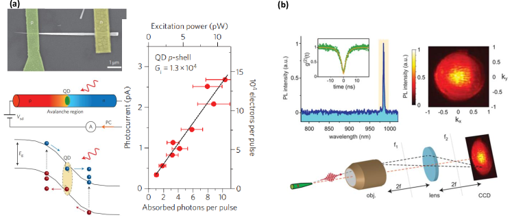
Besides promising emission properties, QDs can also be used for single-photon detection [47]. In principle, QD-based detectors, when designed appropriately, can be sensitive to a wide range of wavelengths, extending to the mid-infrared [48]. Recently, semiconductor nanowire-based light detectors have shown very promising detection performances [49]. Nanowires, when utilized as in-plane light detectors (integrated with the plane of photonic circuits), have the added advantage of being compatible with integrated photonics [50, 51]. An example of such a detector is shown in figure 1(a). Semiconductor nanowire detectors still have a long way to go to match the performance metrics of other on-chip single-photon detection technologies (such as superconducting nanowires, which will be covered in section 3), but thanks to their potential room temperature operation condition and compatibility with monolithic integration techniques, they hold great promises for future integrated quantum photonics.
3 Integrated nanowire single-photon detectors
The inception of superconducting nanowires for single-photon detection dates back to 2001 [52]. Since then, the superconducting nanowire single-photon detectors (SNSPDs) field has witnessed great progress and improvement, mostly with standard fiber-coupled devices [17]. The working principle of on-chip integrated SNSPDs is the same as conventional fiber-coupled detectors [53], typically superconducting nanowires are DC-current biased below their critical current and temperature Tc and when a photon is absorbed, cooper pairs are broken thus quasi-particles (and/or vortices) are created. This leads to the formation of a normal-conducting region in the wire, redirecting the current toward the readout electronics. After a certain recovery time, the superconducting nanowires return to their superconducting state, and the dynamics of this process depend on the kinetic inductance of the device and the readout circuitry.
However, fiber-coupled SNSPDs are not favorable for scaling up detector numbers and lowering the cost per detection channel. For many quantum optics experiments, detectors are usually separately placed in a closed-cycle cryostat, which increases the total cost of targeted applications [54, 4, 55]. Integrating multiple SNSPDs on-chip would enable large-scale on-chip quantum optics experiments with a more compact chip-scale design and fabrication.
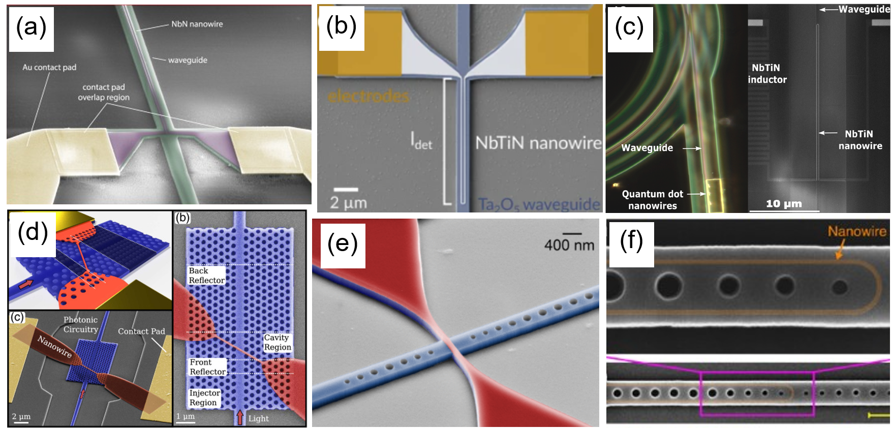
In recent years, great efforts have been put into the integration of large numbers of single-photon detectors on-chip. Unlike traditional fiber-coupled SNSPDs [62], in order to achieve high detection efficiency, SNSPDs are either integrated into photonic waveguides with traveling wave geometry [63, 64], or placed in planar photonic crystal cavities [60, 59]. SNSPDs are typically placed atop optical waveguides and the traveling light field is absorbed by sufficient long superconducting nanowires. This requires depositing superconducting thin films on top of the waveguide layer and then performing electron beam lithography followed by etching steps; An alternative approach is to embed the superconducting nanowires into optical waveguides. As shown in [58], SNSPDs can first be fabricated and tested, and then the optical waveguides can be deterministically formed (deposited and patterned) to integrate with pre-selected SNSPDs.
When designing on-chip SNSPDs, the main concerns include choosing materials, and fabrication routine as described in the following section 4. Due to the small footprint and lower kinetic inductance of the on-chip SNSPDs, these detectors can exhibit faster (sub-nanosecond [59]) recovery time and a lower dark count rate compared to fiber-coupled devices. Also, since the total length of integrated nanowires is significantly shorter, the probability of introducing imperfections is reduced thus a higher yield can be expected. In the future, we expect large numbers of SNSPDs or SNSPD cameras to be integrated into quantum photonic chips for achieving more sophisticated tasks. For a more detailed review of the on-chip integration of SNSPDs with different types of waveguides and their performance, interested researchers are referred to [65]. In the future, besides deploying large numbers of detectors on-chip, how to read out the detection signals of thousands of detection channels remains as an outstanding challenge. In section 6.1, we propose a hybrid integration architecture, which utilizes both the advantage of photonics and electronics technology to overcome the signal read-out challenge.
4 Material and fabrication for quantum emitters and detectors
In this section, we summarize representative material candidates and the general fabrication process for integrated QDs emitters and superconducting nanowire single-photon detectors. Also, we highlighted different hybrid nanowire device integration approaches, and focus on the integration methods and their challenges and advantages in terms of selectivity and scalability.
4.1 Epitaxial growth of nanowire quantum dot
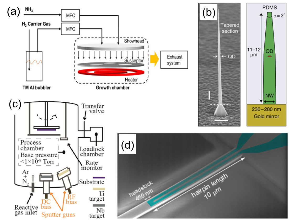
Semiconductor quantum dots have been systematically studied as single-photon sources in various quantum optics applications. They are typically fabricated with top-down or bottom-up approaches. Epitaxial methods, for example, molecular-beam epitaxy (MBE) or Metalorganic vapor-phase epitaxy (MOVPE) [66, 67] are frequently used for growing nanowire QDs. During the epitaxial process, short segments of smaller-band-gap semiconductors are embedded in a larger-band-gap semiconductor. Taking the InAsP QD in InP nanowire as an example [68]: InP nanowires were first grown on InP substrate in an MOVPE reactor with Au particles as catalyst and trimethyl-indium plus phosphine as precursors. Afterward, an InAsP quantum dot was incorporated by introducing As in the reactor using an Arsine flux. Afterward, the chamber temperature was raised to favor radial versus axial growth, thus forming the InP shells. By controlling growth time and temperature, the nanowire geometry is shaped with an optimum nanowire diameter and tapering angle towards the tip. With the tapered waveguide structure, such QDs have high photon extraction efficiency. Each QDs nanowire can be individually tested and transferred following optical measurements to select the best quantum dots on photonic chips for more advanced quantum optics measurements and integration in complex architectures. For more detailed material and fabrication methods regarding nanowire QDs, we refer to [69].
4.2 Superconducting film deposition and detector integration
For superconducting nanowire single-photon detectors, the most commonly used film deposition technology is magnetron sputtering. It is a physical vapor deposition (PVD) process, where a magnetically confined plasma is created near the surface of a target material (e.g. Titanium or Niobium). Positively charged energetic ions from the plasma collide with the negatively charged target material, and atoms from the target are “sputtered”, and then deposit onto the substrate [70]. A single target made of alloys or multiples targets each containing an elementary material can be used for thin superconducting film deposition. Afterward, with one-step electron beam lithography followed by reactive ion etching, the nanowire pattern is created on different substrates previously chosen for sputtering. An alternate approach is to fabricate and pre-test the superconducting nanowires, then deposit waveguide materials on top and selectively etch them to cover the detectors with waveguides [58]. Due to the shorter lengths of integrated superconducting nanowires and thus fewer imperfections, the yield, and recovery time of on-chip detectors can be significantly improved.
4.3 Hybrid integration of quantum emitters and detectors
Given the variety of the needed building blocks for single photon generation to manipulation and detection, a monolithic material platform will not be sufficient to realize complex photonic systems. Recently, there has been a rapid development in hybrid photonic integration approaches. Nanowire quantum emitters pioneered the field of hybrid quantum photonic integration[71]. The geometry of nanowires not only allows for efficient light extraction[68, 35], single-photon detection [51] and electroluminescence [72] 1, but also enables their transfer from the growth chip to other materials and platforms, such as piezoelectric crystals and silicon-based photonic circuits[38, 73, 37, 58, 74, 75]. Two methods of transfer can be used: non-selective through dispersing the nanowires randomly on a target sample and then building the photo-electronic circuitry that incorporates the nanowires using lithographic techniques [76], or selective site-controlled technique using pick and place transfer[38]. In the latter, a typical setup consists of a tungsten needle with a 100 nm tip diameter mounted on a high-precision XYZ stage. The needle can be controlled to adhere to a specific nanowire on the growth chip through van der Waals forces. Then, the tip is used to break the nanowire from the growth chip and transfer it to the target chip with a marker field for further alignment in subsequent fabrication steps. In addition to the pick-and-place technique, transfer printing approaches were also developed [77, 78]. Using a high-precision positioning system, a rubber stamp composed of polydimethylsiloxane (PDMS) can be used to transfer suspended structures from a growth chip to a target. While pick-and-place and transfer printing techniques offer high selectivity of the target quantum emitter in terms of emission line width and wavelength, the scalability is limited, as each quantum emitter has to be mechanically transferred to the target chip. Another promising approach, which over larger scalability, at the expense of selectivity, is the wafer bonding approach. III-V epitaxially produced QD sources have been successfully bonded to silicon nitride photonic chips using this technology[79]. Then using mechanical grinding, chemical mechanical polishing, or chemical etching, the sacrificial layer is removed once the bonding has occurred to reveal the photonic circuit layer. For more details about hybrid integration, we refer the readers to [80, 7]. Finally, hybrid integration was not only limited to quantum emitters, recently, SNSPD hybrid integration was also realized with 100 yield. In the future, interfaces between SNSPDs and external electronic will be necessary for the coupling of SNSPDs with intricate, dynamically reconfigurable photonic structures for active feedback operations.
| Quantum dots in nanowire single-photon emitters | |||
| Materials | Fabrication method | Key performance | Reference |
| \@BTrule[]InAs/GaAs | Solid-source MBE | Emission at 1300 nm | [81] |
| InAsP/InP | Chemical beam epitaxy | Emission 880-1550 nm | [34] |
| InAsP/InP | MOVPE | Light-extraction efficiency of 42% | [68] |
| InAsP/InP | Chemical beam epitaxy | High-fidelity entangled photon-pairs | [29] |
| InAsP/InP | Vapor–liquid-solid (VLS) epitaxy | Multi-photon event <1% | [82] |
| AlGaAs/GaAs | MBE | Background-free | [24] |
| GaAsP/GaP | Low-pressure MOVPE | Bright QDs grown on Si substrate | [83] |
| InGaN/GaN | Plasma-assisted MBE | Electrically driven QDs | [84] |
| InGaAs/GaAs | MOCVD | Strain-engineered telecom wavelength DQs | [85] |
| AlGaN/GaN | MOCVD | Room-temperature operation with | [86] |
| \@BTrule[] Superconducting nanowire single-photon detectons | |||
| Materials | Fabrication method | Key performance | Reference |
| \@BTrule[]NbN | Molecular-beam epitaxy (MBE) | Working on AlN circuits | [87] |
| NbN | Atomic layer deposited (ALD) | Working till 2006 nm | [88] |
| NbTiN | Magnetron co-sputtering | >99% efficiency | [62] |
| NbTiN | Magnetron co-sputtering | 7.7ps timing jitter | [89] |
| WSi | Magnetron co-sputtering | 93% efficiency | [90] |
| MoSi | Magnetron co-sputtering | >98% efficiency | [91] |
| NbRe | Magnetron sputtering | Visible-infrared detection | [92] |
| TaN | Magnetron sputtering | Large-area X-ray detection | [93] |
| NbN | Magnetron sputtering | >98% efficiency | [94] |
| MgB2 | Hybrid physical chemical vapor deposition | 130 ps relaxation time | [95] |
5 Emerging quantum photonic technology and outlooks
In this section, we highlight a non-exhaustive number of established and emerging quantum optics applications enabled by (partially) integrating quantum emitters, waveguides, and detectors on-chip. We also present perspectives on future quantum technologies with their benchmarks and targets using integrated quantum photonic technology.
5.1 Photonic boson sampling
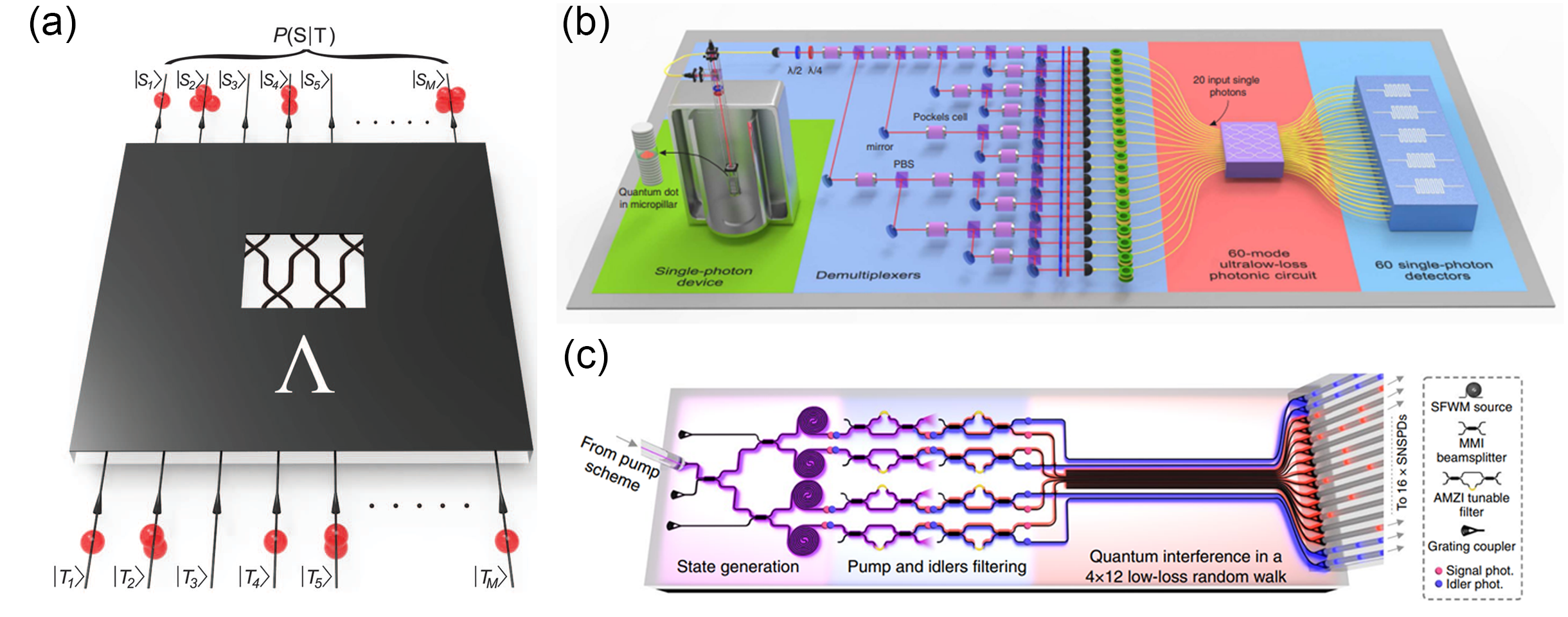
Boson sampling, first proposed by Scott Aaronson and Alex Arkhipov [101], is a computational task aiming to demonstrate quantum advantage with an intermediate-scale quantum device. The central idea of the task is to sample the output distribution of indistinguishable bosons interfering in a linear network, as schematically shown in figure 4(a). With the increase of photon numbers, the task becomes intractable using the classical computation approach due to the intrinsic hardness of calculating the matrix permanent, and thus is considered an excellent candidate to demonstrate quantum computational advantage [102]. To this end, the photonic system is one of the most suitable platforms, as the key elements (quantum emitters, linear state evolution, and single-photon detectors) are widely available with the current technology as described in the previous sections 2 and 3.
As the early demonstrations of boson sampling, several research groups have chosen to use photon pairs generated from spontaneous parametric down-conversion process and silica photonic chips [98, 103, 104, 105]. To overcome the low generation rate issue from probabilistic photon sources, some research groups chose semiconductor quantum dot emitter as the input states [54, 106], thus the photon number was dramatically increased from the initial 3 to 20 photons with a state space dimension up to 1014 [99]. The experimental setup shown in figure 4(b) represents the largest scale of boson sampling using quantum dot emitter and SNSPD detection. In the meanwhile, a variant of boson sampling was proposed to use a single mode squeezed vacuum state as the input state instead of the Fock state, called Gaussian boson sampling [107, 108]. Unlike the original boson sampling protocol, where photon numbers are conserved, Gaussian boson sampling offers a boost in the photon number since the source could emit random numbers of photon pairs. Gaussian boson sampling has been experimentally demonstrated using both ultra-low loss bulk optics [4, 55] and silicon photonics platform [100]. Figure 4(c) demonstrates the design of the integrated photonics circuit, unlike the bulk optics setup, the chip has a rather small footprint and could be extended to a large-scale device. Nonlinear effects in silicon can naturally generate photon pairs via spontaneous four-wave mixing in either spiral waveguides [109] or ring resonators [110, 111]. It is still an open question whether the current technology is capable of scaling boson sampling to arbitrarily large dimensions while maintaining the quantum advantage. Also, such ultra-large-scale experiments require huge numbers of single-photon detectors and the corresponding coincidence detection systems, e.g. distributed SNSPDs with cryogenics and control electronics, making them far from cost-effective [112]. As a result, integrated photonics technology is commonly believed to be a promising approach to reaching scalable boson sampling [113]. In addition, the optical modes of Gaussian boson sampling can be mapped to vibrational normal modes to solve the vibronic spectrum of a molecule [114]. Gaussian boson sampling also holds the potential to solve graph theory problems [115, 116] and molecular docking for pharmaceutical drug design [117]. The on-chip photonic circuits potentially possess higher stability (e.g. less phase drift and frequency drift), better isolation from the environment, and low power consumption to be programmable [118] to solve the challenging applications we mentioned above. With the advances in integrated photonics technology, nowadays larger modular linear optical circuits [119], bright quantum emitters [68] and controlled integration of detectors [58] are more widely available, thus a scalable integrated boson sampler for specific practical problems is the next step to be achieved.
5.2 Quantum walks
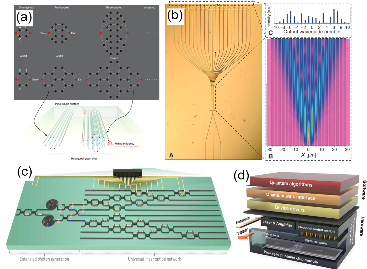
Quantum walks are the quantum counterparts of classical random walks first proposed in 1993[124], where quantum superposition plays an extremely important role. Unlike a classical particle, a quantum particle can simultaneously propagate in different directions, and this unique behavior leads to the ballistic transport feature of the quantum walk. Normally, there are two different models of quantum walks, namely discrete quantum walks, and continuous quantum walks. Depending on the tasks, quantum walks could provide either exponential (quantum fast-hitting) [125, 120] or polynomial (quantum search algorithm) [126, 127] speedup over classical algorithms [128], and could even implement universal quantum computation [129, 130]. The photon, which inherently exhibits the wave-particle duality, is naturally a good candidate as a "walker". The quantum properties of photons including superposition, quantum interference, and entanglement can be employed to perform various quantum walk experiments. Early-stage quantum walk experiments are conducted by the bulk optics beam splitters [131] and fiber loops [132, 133] in the time domain. As a comparison, integrated circuits offer higher phase stability, thus further leading to a higher level of integration [121, 134, 135]. For example, figure 5(a) illustrates the implementation of a quantum walk with a glued binary tree structure on photonic chips using femtosecond laser-written waveguide arrays, and figure 5(b) demonstrates a continuously coupled waveguide array for realizing correlated photon quantum walks. Similarly, in figure 5(c), an integrated photonic platform consisting of reconfigurable linear optical networks and controllable on-chip entangled photon pair sources, demonstrates the simulation of thousands of continuous-time quantum walk evolutions [122]. Most recently, a full-stack quantum walk processor based on an integrated photonic chip is used to demonstrate a series of quantum applications, from graph-theoretic applications to quantum simulations of topological phases [123] as shown in figure 5(d).
5.3 On-chip quantum communication
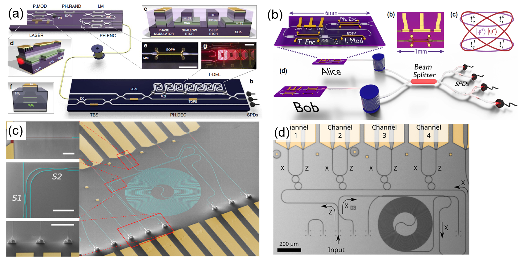
Unconditional secure information exchange is a demanding requirement for both governments and individuals. Over the past few decades, quantum key distribution (QKD) with security fundamentally guaranteed by the laws of physics, has grown rapidly from lab demonstrations to the deployment of commercially available systems connecting distant cities. Demonstrated by the recently launched quantum satellite, space-to-ground QKD has linked locations over 1200 km apart [140, 141, 142], and even intercontinental quantum communication over 7600 km [143] has been realized. In general, a QKD system includes a signal-sending part for generating required photon states and a signal-receiving part for photon state detection. Integration efforts have been made to lower the size, cost, and energy consumption of both ends. Ideally, a "sender chip" using integrated light sources with polarization modulators, phase modulators, and power attenuators could efficiently generate certain photon states (e.g. BB84 with polarization or phase encoding), while a "receiver chip" integrated with many single-photon detectors, optical circuits, and control electronics could register the signal photons to decode the information [144, 137]. There have been several experimental demonstrations of silicon photonic transmitters for polarization [145], time-bins [146, 136] and space division multiplexing encoding [147]. An intercity metropolitan QKD test was performed using a silicon photonics encoder, reaching a quantum communication distance over 42 km [148]. Another recent experiment using silicon photonics realized the chip-based transmitter and receiver for continuous-variable QKD [149]. In a recent demonstration, a four-channel silicon nitride-based integrated QKD receiver achieved a total secret-key rate of up to 12.17 Mbit/s at a 3.35 GHz clock rate using wavelength-division de-multiplexing and waveguide-integrated superconducting nanowire single-photon detectors [139]. Besides QKD, chip-based quantum teleportation has also been demonstrated using an integrated photonics platform [150]. For more detailed QKD-related protocols, implementation, security analysis, and attacking risks, the reader can refer to [151, 152].
5.4 Optical neural networks for machine learning
In the era of big data, artificial intelligence has greatly revolutionized the modern world and has applications in many areas, for example, image and language analysis, self-driving vehicles, and the famous alpha Go [153]. Currently, electronic circuits are still the prevailing computing power support for artificial intelligence, especially promoted by GPU calculations, however, the Von Neumann architecture cannot meet the increasing demand for ultra-large-scale information processing, limited by energy consumption and electronic interference [154, 155]. Light, as an excellent information carrier, which travels with fast speed and high parallelism, can solve electronic defects and the research of optical neural network (ONN) can boost the development of artificial intelligence with energy and time efficiency [156, 157].

The optical implementation of neural networks basically contains two parts: linear operation and nonlinear activation, which can be seen as linear multiplication and summation operations, as shown in figure 7(a), where a complex-valued neuron is implemented by a mesh of MZI [158]. In a fully connected linear network, each neuron in the output layer is a weighted sum of all input neurons — which can be mathematically represented as a matrix-vector multiplication. Such multiply-accumulate operations can be experimentally implemented by meshes of Mach–Zehnder interferometers (MZIs), as in reference [159] and figure 7(b). The central idea is to use the principle of interference to implement linear operations, with the tunability of phase shifters in MZIs, the ONN can implement any operation on the input states. Normally the demanding resources (such as MZIs) for a dimension input is , recently, space-efficient integrated diffractive cells are demonstrated [161] to further reduce footprint and energy consumption. Nowadays, on-chip ONNs have been extensively realized for the prediction of molecular properties [162], graph representation learning [163], noise-resilient learning [164], bacterial foraging training [165], and image classification [166]. In recent research, in situ training of ONNs was realized by a fully-integrated coherent optical neural network, including integrated coherent transmitter, matrix multiplication unit, nonlinear function unit and on-chip detection [167]. To push the physical limit of energy efficiency, a novel spiking neural network was recently demonstrated to perform neuromorphic computing[160, 168] using the combination of integrated photonics and SNSPDs, as shown in figure 7(c). Such a device has the potential to perform 10 times more operations compared to the human brain with much less energy cost. Another great advance in the field of optical neural networks is the emergence of quantum machine learning [169, 170]. With unique quantum features like superposition and entanglement, quantum machine learning algorithms can outperform their classical counterpart with faster speed and fewer resources [171, 172, 173, 174, 175].
5.5 Integrated quantum Lidar system
Light detection and ranging, known as "Lidar", is a powerful technology for environmental monitoring, remote target recognition, forest mapping on the earth's surface, and sea fog measurements on ocean[176, 177, 178, 179]. It detects scattered or reflected light to acquire distance or depth information of remote targets. Typically, a Lidar system consists of pulse laser sources, beam splitters, transceivers, time-correlated single-photon counting electronics, and photodetectors. With the increase in measurement distance, after tens of kilometers, only a few photons can travel back to the detection end, thus the use of single photon detectors can efficiently improve Lidar systems' detection range, depth accuracy, and acquisition time. The superconducting nanowire single-photon detectors developed in the past decades with high efficiency, low timing jitter, and dark count rates [17] are becoming the popular choice for recent Lidar systems. A comprehensive review of SNSPD-based Lidars can be found in [180]. In the coming future, photon number resolving detectors and efficient mid-infrared detectors will open new detection windows and capabilities for Lidar systems [181]. Also, with the development of high-power on-chip laser, photonic integrated circuits, and detector technology, monolithic Lidar chips would enable more compact, space-compatible Lidar applications in the future [182, 183].
5.6 Meta-surface for integrated quantum optics circuits
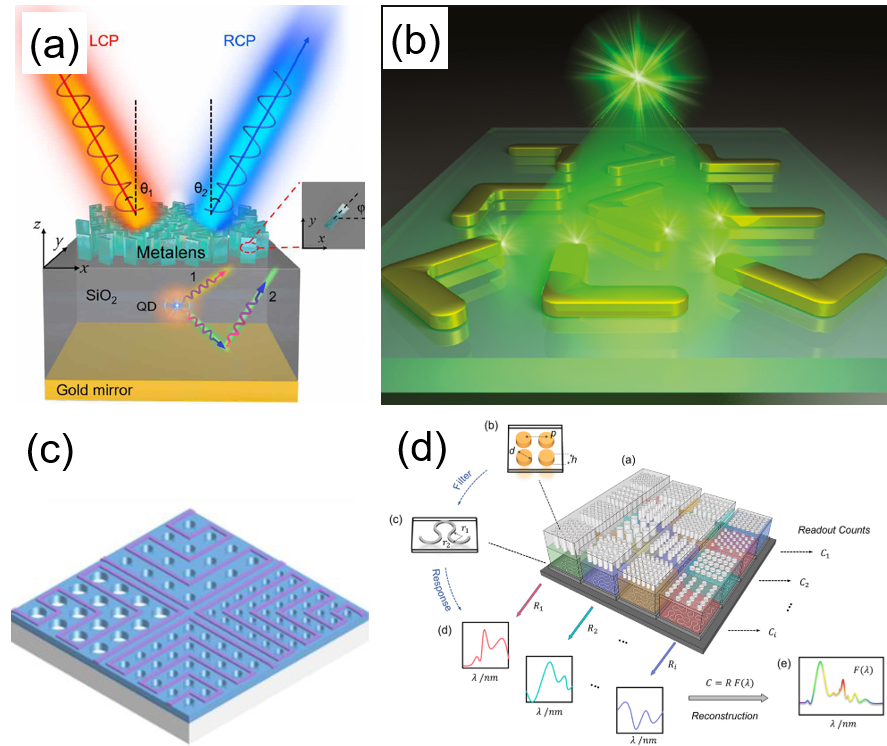
With the improvement of high-precision nanofabrication, recent years have seen great progress and increased interest in the field of metasurfaces, which typically contain periodic sub-wavelength metallic/dielectric structures that resonantly couple to the electric and magnetic fields of the light wave [184, 185]. Metasurfaces offer unique solutions to realize unconventional phenomena, for example, negative refraction, achromatic focusing, and electromagnetic cloaking [186, 187, 188]. The applications of metasurfaces have also been extended from traditional optics to quantum optics, where single photons sources, entangled photons, and single-photon detection are fundamentally required. For the quantum dots emitters described in section 2, the random photon emission issue compromises their use and especially hinders the on-demand manipulation of their spin states. As shown in [189] integrating QDs with metasurface leads to on-demand generation and separation of the spin states of the emitted single photons along any arbitrary engineered direction. Also, Purcell enhancement can be realized using meta-surface with QDs [190]. When combining metasurface with superconducting nanowire single-photon detectors as described in section 3, the functionality of these quantum detectors can be greatly extended, for example, achieving spectrum reconstruction on chip [191, 192]. In the future, combining metasurface with quantum optics elements on-chip will offer new possibilities for controlling single-photon emission, single-photon state manipulation, and single-photon detection and imaging. For more detailed integrated metasurface applications in quantum optics, we refer to [193].
6 Outlooks on future quantum photonics technologies
After decades of development, integrated (quantum) photonics—the science and technology of generating, controlling, and detecting photons on a chip scale-has benefited different industries and society. For example, in telecommunications, where bandwidth and security are greatly demanded and photonic integrated circuits (PICs) offer a viable solution; Other emerging application areas, including quantum photonic computing, bio-photonics sensing, environmental monitoring, and disease diagnosis are also witnessing game-changing breakthroughs triggered by the rapid development of quantum integrated photonic technology. Here, we present two promising envisioned photonic circuit experiments that could further boost the impact of nanowire-based integrated photonics in science and technology.
6.1 On-chip quantum information processing
Recently, the design and production of integrated photonics started to merge into the mainstream of the electronic industry. Such hybrid chips [71] take the complementary advantages of both platforms to perform sophisticated tasks. As illustrated in figure 9, the hybrid photonic/electronic integrated circuit contains optically pumped (green) and electrically driven (red) nanowire QDs as single-photon sources. After emission, the photon states can be tuned by additional on-chip elements (e.g. phase shifters [194]). Multiple photons with precisely controlled initial states are then ejected into the linear interferometer to interact with different photonic quantum computing or simulation protocols. Afterward, the output results (photons) are registered by multi-channels on-chip SNSPDs with integrated control CMOS circuits and time-to-digital (TDC) converters. Such a hybrid chip can be mounted in a compact cryostat without using many coaxial cables, which helps to improve system scalability and reduce the total heat load. In the future, to realize mass production of such proposed hybrid chips, each containing millions of elements, electronics, CMOS-compatible optics, and dedicated superconductor fabrication are simultaneously needed at a foundry level. Also, automatic pre-testing equipment of such chips is significantly important to be developed (e.g. cryogenic probe station [195]), where artificial intelligence algorithms can also help to improve failure analysis [196].

6.2 On-chip quantum bio-sensing
Different classes of single-photon emitters have been employed for bio-photonic imaging and spectroscopy. Each of these emitters has its own advantages and weaknesses. To this end, quantum dots were among the first emitters to be explored and have already come a long way. Most commonly in biomedical applications and fluorescence microscopy, quantum dots (and in general single-photon emitters) are utilized as biomarkers [197, 198, 199, 200, 201] in which their position (localization), color, brightness, lifetime, etc. is linked to a certain biological/chemical factor. Among the important remaining challenges ahead of bio-quantum sensing with quantum dots are chemical toxicity and optical attenuation, i.e. the light from the emitter is highly attenuated by the tissue before reaching the detection optics. Infrared quantum dots can benefit from enhanced transparency of the tissue. Synthesis of high-quality infrared emitting quantum dots [202, 203] as well as efficient and precise detection of those photons [204, 205] have achieved promising results but require further progress. High quantum yield emitters as well as sensitive and low noise detectors with a large active area can further boost the impact of infrared bio-imaging.
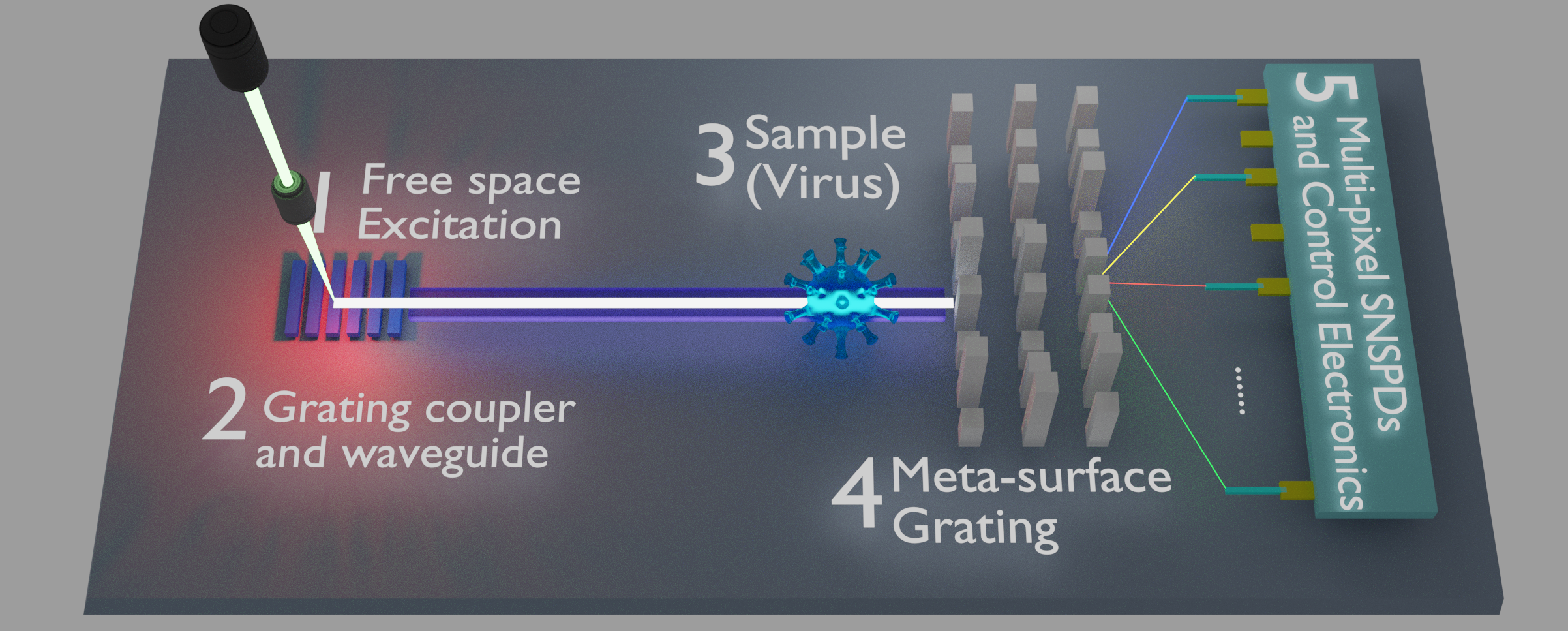
As described in the previous sections, integrated photonic circuits can generate, transmit, and detect a broad band of optical signals on-chip. This naturally offers the ability to simultaneously detect and identify different biological objects (e.g. single-virus [206], proteins [207], single-molecule [208]), which is one of the key requirements for disease diagnostic and drug developments.
Integrated photonic circuits can help to create such a highly sensitive, multi-functional platform on a chip scale. Also, by using single-photon detectors, the sensitivity of such systems can be improved to reach their quantum limits. As depicted in figure 10, a broadband excitation light signal transmits from free space to the chip with the help of efficient grating couplers. The waveguide delivers light to the samples under test (a virus in this case). Afterward, the transmitted or scattered photon signal pass through the meta-surface grating to acquire spectral information with multi-pixel SNSPDs at the detection ports. With precise spectral information, the identity or structure of bio-samples can be efficiently acquired. Such chips hold great potential in both scientific labs and biochemical industries, and again, nanowire-based devices are the key enabling elements in the proposed systems.
7 Conclusion and future perspectives
With the 2022 Nobel physics prize awarded to the scientists who opened the quantum optics field using single-photons and entangled photon pairs, the field of quantum photonics science is expected to gain more attention. After decades of development, this field has witnessed great developments in both fundamental theory and real-world applications. The applications of nanowires QDs and SNSPDs are extending from proof-of-principle demonstrations to large-scale quantum computing, quantum simulation, and quantum sensing. Integrated and hybrid quantum photonic solutions are promising approaches for developing next-generation quantum hardware, where the advantages of photonics, electronics, and condensed matter physics can be combined for game-changing innovations. Looking into the future, there are still important challenges to be addressed:
-
–
From quantum emitters' perspective, To interface the flying qubits with the current optical fiber network, quantum emitters must be developed that operate at the telecommunication wavelength of 1550 nm. A further benefit of this advancement is enabling hybrid integration to silicon on insulator photonics, the most developed photonic platform for both classical and quantum applications. Additionally, one key objective is to interface several nanowire QDs, so that they may be used as solid-state quantum memories, and each may function as a quantum node for communication purposes. Such target application would require Fourier-limited emission and more stringent control over the emission wavelength spread in nanowire quantum dot samples. Lastly, higher photon indistinguishability without time-gating or post-processing is key for several applications highlighted in this review.
-
–
On the detection side, significant advancements have recently been made, allowing SNSPDs to be used in new fields including biological imaging. Following this advancement, it may be advantageous to realize SNSPDs at longer wavelength ranges. This should be done in collaboration with researchers developing biological markers to maximize the detectors' qualities in the desired wavelength range. Additionally, even though large-scale SNSPD arrays have made significant progress, additional work is still required to realize SNDPD 2D cameras with individual pixel-readout circuitry solutions. In the realms of optical imaging, sensing, and biology, this will be a game-changer. Also, a better understanding of how the superconducting films' material properties influence their photon detection performance will help to improve SNSPDs' yield, and ultimately bring down the cost of this technology. This will advance the commercialization of SNSPDs and expand their use to as-yet-untapped markets and research areas.
To conclude, through a systematic review of the theory, material platform, and fabrication process of the nanowires, this paper serves as a solid reference for both young and senior researchers in the integrated quantum photonics field. Additionally, we propose promising quantum photonics architectures and sensing experiments and aim at attracting a wider range of readers and invoking more collaborations between researchers in different fields.
Bibliography
- [1] Gilbert Grynberg, Alain Aspect, Claude Fabre, and Claude Cohen-Tannoudji. Introduction to Quantum Optics: From the Semi-classical Approach to Quantized Light. Cambridge University Press, 2010.
- [2] Christopher Gerry and Peter Knight. Introductory Quantum Optics. Cambridge University Press, 2004.
- [3] M. Fox. Quantum Optics: An Introduction. Oxford Master Series in Physics. OUP Oxford, 2006.
- [4] Han-Sen Zhong, Hui Wang, Yu-Hao Deng, Ming-Cheng Chen, Li-Chao Peng, Yi-Han Luo, Jian Qin, Dian Wu, Xing Ding, Yi Hu, et al. Quantum computational advantage using photons. Science, 370(6523):1460–1463, 2020.
- [5] S. Tanzilli, A. Martin, F. Kaiser, M.P. De Micheli, O. Alibart, and D.B. Ostrowsky. On the genesis and evolution of integrated quantum optics. Laser & Photonics Reviews, 6(1):115–143, 2012.
- [6] Fulvio Flamini, Nicolò Spagnolo, and Fabio Sciarrino. Photonic quantum information processing: a review. Reports on Progress in Physics, 82(1):016001, nov 2018.
- [7] Ali W. Elshaari, Wolfram Pernice, Kartik Srinivasan, Oliver Benson, and Val Zwiller. Hybrid integrated quantum photonic circuits. Nature Photonics, 14(5):285–298, May 2020.
- [8] Galan Moody, Volker J Sorger, Daniel J Blumenthal, Paul W Juodawlkis, William Loh, Cheryl Sorace-Agaskar, Alex E Jones, Krishna C Balram, Jonathan C F Matthews, Anthony Laing, Marcelo Davanco, Lin Chang, John E Bowers, Niels Quack, Christophe Galland, Igor Aharonovich, Martin A Wolff, Carsten Schuck, Neil Sinclair, Marko Lončar, Tin Komljenovic, David Weld, Shayan Mookherjea, Sonia Buckley, Marina Radulaski, Stephan Reitzenstein, Benjamin Pingault, Bartholomeus Machielse, Debsuvra Mukhopadhyay, Alexey Akimov, Aleksei Zheltikov, Girish S Agarwal, Kartik Srinivasan, Juanjuan Lu, Hong X Tang, Wentao Jiang, Timothy P McKenna, Amir H Safavi-Naeini, Stephan Steinhauer, Ali W Elshaari, Val Zwiller, Paul S Davids, Nicholas Martinez, Michael Gehl, John Chiaverini, Karan K Mehta, Jacquiline Romero, Navin B Lingaraju, Andrew M Weiner, Daniel Peace, Robert Cernansky, Mirko Lobino, Eleni Diamanti, Luis Trigo Vidarte, and Ryan M Camacho. 2022 roadmap on integrated quantum photonics. Journal of Physics: Photonics, 4(1):012501, jan 2022.
- [9] Jacques Carolan, Christopher Harrold, Chris Sparrow, Enrique Martín-López, Nicholas J. Russell, Joshua W. Silverstone, Peter J. Shadbolt, Nobuyuki Matsuda, Manabu Oguma, Mikitaka Itoh, Graham D. Marshall, Mark G. Thompson, Jonathan C. F. Matthews, Toshikazu Hashimoto, Jeremy L. O’Brien, and Anthony Laing. Universal linear optics. Science, 349(6249):711–716, 2015.
- [10] Ben Bartlett and Shanhui Fan. Universal programmable photonic architecture for quantum information processing. Phys. Rev. A, 101:042319, Apr 2020.
- [11] Peter Lodahl. Quantum-dot based photonic quantum networks. Quantum Science and Technology, 3(1):013001, oct 2017.
- [12] Benjamin J. Metcalf, Justin B. Spring, Peter C. Humphreys, Nicholas Thomas-Peter, Marco Barbieri, W. Steven Kolthammer, Xian-Min Jin, Nathan K. Langford, Dmytro Kundys, James C. Gates, Brian J. Smith, Peter G. R. Smith, and Ian A. Walmsley. Quantum teleportation on a photonic chip. Nature Photonics, 8(10):770–774, Oct 2014.
- [13] P. Zhang, K. Aungskunsiri, E. Martín-López, J. Wabnig, M. Lobino, R. W. Nock, J. Munns, D. Bonneau, P. Jiang, H. W. Li, A. Laing, J. G. Rarity, A. O. Niskanen, M. G. Thompson, and J. L. O'Brien. Reference-frame-independent quantum-key-distribution server with a telecom tether for an on-chip client. Phys. Rev. Lett., 112:130501, Apr 2014.
- [14] Jianwei Wang, Fabio Sciarrino, Anthony Laing, and Mark G. Thompson. Integrated photonic quantum technologies. Nature Photonics, 14(5):273–284, May 2020.
- [15] M. D. Eisaman, J. Fan, A. Migdall, and S. V. Polyakov. Invited review article: Single-photon sources and detectors. Review of Scientific Instruments, 82(7):071101, 2011.
- [16] Evan Meyer-Scott, Christine Silberhorn, and Alan Migdall. Single-photon sources: Approaching the ideal through multiplexing. Review of Scientific Instruments, 91(4):041101, 2020.
- [17] Iman Esmaeil Zadeh, J Chang, Johannes WN Los, Samuel Gyger, Ali W Elshaari, Stephan Steinhauer, Sander N Dorenbos, and Val Zwiller. Superconducting nanowire single-photon detectors: A perspective on evolution, state-of-the-art, future developments, and applications. Applied Physics Letters, 118(19):190502, 2021.
- [18] Igor Aharonovich, Dirk Englund, and Milos Toth. Solid-state single-photon emitters. Nature Photonics, 10(10):631–641, 2016.
- [19] X He, H Htoon, SK Doorn, WHP Pernice, F Pyatkov, R Krupke, A Jeantet, Y Chassagneux, and C Voisin. Carbon nanotubes as emerging quantum-light sources. Nature materials, 17(8):663–670, 2018.
- [20] Yasuhiko Arakawa and Mark J Holmes. Progress in quantum-dot single photon sources for quantum information technologies: A broad spectrum overview. Applied Physics Reviews, 7(2):021309, 2020.
- [21] Milos Toth and Igor Aharonovich. Single photon sources in atomically thin materials. Annual review of physical chemistry, 70:123–142, 2019.
- [22] Niccolo Somaschi, Valerian Giesz, Lorenzo De Santis, JC Loredo, Marcelo P Almeida, Gaston Hornecker, S Luca Portalupi, Thomas Grange, Carlos Anton, Justin Demory, et al. Near-optimal single-photon sources in the solid state. Nature Photonics, 10(5):340–345, 2016.
- [23] Natasha Tomm, Alisa Javadi, Nadia Olympia Antoniadis, Daniel Najer, Matthias Christian Löbl, Alexander Rolf Korsch, Rüdiger Schott, Sascha René Valentin, Andreas Dirk Wieck, Arne Ludwig, et al. A bright and fast source of coherent single photons. Nature Nanotechnology, 16(4):399–403, 2021.
- [24] Lucas Schweickert, Klaus D Jöns, Katharina D Zeuner, Saimon Filipe Covre da Silva, Huiying Huang, Thomas Lettner, Marcus Reindl, Julien Zichi, Rinaldo Trotta, Armando Rastelli, et al. On-demand generation of background-free single photons from a solid-state source. Applied Physics Letters, 112(9):093106, 2018.
- [25] Xing Ding, Yu He, Z-C Duan, Niels Gregersen, M-C Chen, S Unsleber, Sebastian Maier, Christian Schneider, Martin Kamp, Sven Höfling, et al. On-demand single photons with high extraction efficiency and near-unity indistinguishability from a resonantly driven quantum dot in a micropillar. Physical review letters, 116(2):020401, 2016.
- [26] Hui Wang, Yu He, Yu-Huai Li, Zu-En Su, Bo Li, He-Liang Huang, Xing Ding, Ming-Cheng Chen, Chang Liu, Jian Qin, et al. High-efficiency multiphoton boson sampling. Nature Photonics, 11(6):361–365, 2017.
- [27] Michael E Reimer, Gabriele Bulgarini, Nika Akopian, Moïra Hocevar, Maaike Bouwes Bavinck, Marcel A Verheijen, Erik PAM Bakkers, Leo P Kouwenhoven, and Val Zwiller. Bright single-photon sources in bottom-up tailored nanowires. Nature communications, 3(1):1–6, 2012.
- [28] Ranber Singh and Gabriel Bester. Nanowire quantum dots as an ideal source of entangled photon pairs. Physical review letters, 103(6):063601, 2009.
- [29] Marijn AM Versteegh, Michael E Reimer, Klaus D Jöns, Dan Dalacu, Philip J Poole, Angelo Gulinatti, Andrea Giudice, and Val Zwiller. Observation of strongly entangled photon pairs from a nanowire quantum dot. Nature communications, 5(1):1–6, 2014.
- [30] Patrick Laferrière, Aria Yin, Edith Yeung, Leila Kusmic, Marek Korkusinski, Payman Rasekh, David B Northeast, Sofiane Haffouz, Jean Lapointe, Philip J Poole, et al. Approaching transform-limited photons from nanowire quantum dots excited above-band. arXiv preprint arXiv:2208.00066, 2022.
- [31] Dan Dalacu, Philip J Poole, and Robin L Williams. Nanowire-based sources of non-classical light. Nanotechnology, 30(23):232001, 2019.
- [32] Richard G Hobbs, Nikolay Petkov, and Justin D Holmes. Semiconductor nanowire fabrication by bottom-up and top-down paradigms. Chemistry of Materials, 24(11):1975–1991, 2012.
- [33] Patrick Laferrière, Edith Yeung, Isabelle Miron, David B Northeast, Sofiane Haffouz, Jean Lapointe, Marek Korkusinski, Philip J Poole, Robin L Williams, and Dan Dalacu. Unity yield of deterministically positioned quantum dot single photon sources. Scientific Reports, 12(1):1–9, 2022.
- [34] Sofiane Haffouz, Katharina D Zeuner, Dan Dalacu, Philip J Poole, Jean Lapointe, Daniel Poitras, Khaled Mnaymneh, Xiaohua Wu, Martin Couillard, Marek Korkusinski, et al. Bright single inasp quantum dots at telecom wavelengths in position-controlled inp nanowires: The role of the photonic waveguide. Nano letters, 18(5):3047–3052, 2018.
- [35] Gabriele Bulgarini, Michael E Reimer, Maaike Bouwes Bavinck, Klaus D Jöns, Dan Dalacu, Philip J Poole, Erik PAM Bakkers, and Val Zwiller. Nanowire waveguides launching single photons in a gaussian mode for ideal fiber coupling. Nano letters, 14(7):4102–4106, 2014.
- [36] Patrick Laferriere, Edith Yeung, Lambert Giner, Sofiane Haffouz, Jean Lapointe, Geof C Aers, Philip J Poole, Robin L Williams, and Dan Dalacu. Multiplexed single-photon source based on multiple quantum dots embedded within a single nanowire. Nano letters, 20(5):3688–3693, 2020.
- [37] Ali W Elshaari, Iman Esmaeil Zadeh, Andreas Fognini, Michael E Reimer, Dan Dalacu, Philip J Poole, Val Zwiller, and Klaus D Jöns. On-chip single photon filtering and multiplexing in hybrid quantum photonic circuits. Nature communications, 8(1):1–8, 2017.
- [38] Ali W Elshaari, Efe Büyüközer, Iman Esmaeil Zadeh, Thomas Lettner, Peng Zhao, Eva Schö, Samuel Gyger, Michael E Reimer, Dan Dalacu, Philip J Poole, et al. Strain-tunable quantum integrated photonics. Nano letters, 18(12):7969–7976, 2018.
- [39] Mohd Zeeshan, Nachiket Sherlekar, Arash Ahmadi, Robin L Williams, and Michael E Reimer. Proposed scheme to generate bright entangled photon pairs by application of a quadrupole field to a single quantum dot. Physical review letters, 122(22):227401, 2019.
- [40] Feng Liu, Alistair J Brash, John O’Hara, Luis MPP Martins, Catherine L Phillips, Rikki J Coles, Benjamin Royall, Edmund Clarke, Christopher Bentham, Nikola Prtljaga, et al. High purcell factor generation of indistinguishable on-chip single photons. Nature nanotechnology, 13(9):835–840, 2018.
- [41] Konstantinos G Lagoudakis, Peter L McMahon, Kevin A Fischer, Shruti Puri, Kai Müller, Dan Dalacu, Philip J Poole, Michael E Reimer, Val Zwiller, Yoshihisa Yamamoto, et al. Initialization of a spin qubit in a site-controlled nanowire quantum dot. New Journal of Physics, 18(5):053024, 2016.
- [42] Philipp Aumann, Maximilian Prilmüller, Florian Kappe, Laurin Ostermann, Dan Dalacu, Philip J Poole, Helmut Ritsch, Wolfgang Lechner, and Gregor Weihs. Demonstration and modeling of time-bin entangled photons from a quantum dot in a nanowire. AIP Advances, 12(5):055115, 2022.
- [43] Paul Anderson, Rubayet Al Maruf, Sreesh Venuturumilli, Divya Bharadwaj, Sonell Malik, Jiawei Qiu, Yujia Yuan, Philip Poole, Dan Dalacu, Michael Reimer, et al. Delaying tunable single photons from a quantum dot with an atomic ensemble. In APS Division of Atomic, Molecular and Optical Physics Meeting Abstracts, volume 2022, pages F01–047, 2022.
- [44] Rubayet Al Maruf, Sai Sreesh Venuturumilli, Divya Bharadwaj, Paul Anderson, Jiawei Qiu, Yujia Yuan, Behrooz Semnani, Sonell Malik, Mohd Zeeshan, Dan Dalacu, et al. Single-photon source based on a quantum dot emitting at cesium wavelength. In Optical and Quantum Sensing and Precision Metrology II, volume 12016, pages 239–246. SPIE, 2022.
- [45] Divya Bharadwaj, Paul Anderson, Sreesh Venuturumilli, Rubayet Al Maruf, Jiawei Qiu, Taehyun Yoon, Behrooz Semnani, Yujia Yuan, Jinjin Du, Mohd Zeeshan, et al. Interfacing quantum dots with laser-cooled atomic ensembles. In Optical and Quantum Sensing and Precision Metrology, volume 11700, pages 211–217. SPIE, 2021.
- [46] Yan Chen, Iman Esmaeil Zadeh, Klaus D. Jöns, Andreas Fognini, Michael E. Reimer, Jiaxiang Zhang, Dan Dalacu, Philip J. Poole, Fei Ding, Val Zwiller, and Oliver G. Schmidt. Controlling the exciton energy of a nanowire quantum dot by strain fields. Applied Physics Letters, 108(18):182103, 2016.
- [47] J. C. Blakesley, P. See, A. J. Shields, B. E. Kardynał, P. Atkinson, I. Farrer, and D. A. Ritchie. Efficient single photon detection by quantum dot resonant tunneling diodes. Phys. Rev. Lett., 94:067401, Feb 2005.
- [48] Matthias J. Grotevent, Claudio U. Hail, Sergii Yakunin, Dominik Bachmann, Michel Calame, Dimos Poulikakos, Maksym V. Kovalenko, and Ivan Shorubalko. Colloidal hgte quantum dot/graphene phototransistor with a spectral sensitivity beyond 3 µm. Advanced Science, 8(6):2003360, 2021.
- [49] Sandra J. Gibson, Brad van Kasteren, Burak Tekcan, Yingchao Cui, Dick van Dam, Jos E. M. Haverkort, Erik P. A. M. Bakkers, and Michael E. Reimer. Tapered inp nanowire arrays for efficient broadband high-speed single-photon detection. Nature Nanotechnology, 14(5):473–479, May 2019.
- [50] Linyou Cao, Joon-Shik Park, Pengyu Fan, Bruce Clemens, and Mark L. Brongersma. Resonant germanium nanoantenna photodetectors. Nano Letters, 10(4):1229–1233, 2010. PMID: 20230043.
- [51] Gabriele Bulgarini, Michael E Reimer, Moïra Hocevar, Erik P A M Bakkers, Leo P Kouwenhoven, and Val Zwiller. Avalanche amplification of a single exciton in a semiconductor nanowire. Nature Photonics, 6(7):455–458, jul 2012.
- [52] GN Gol’Tsman, O Okunev, G Chulkova, A Lipatov, A Semenov, K Smirnov, B Voronov, A Dzardanov, C Williams, and Roman Sobolewski. Picosecond superconducting single-photon optical detector. Applied physics letters, 79(6):705–707, 2001.
- [53] Chandra M Natarajan, Michael G Tanner, and Robert H Hadfield. Superconducting nanowire single-photon detectors: physics and applications. Superconductor science and technology, 25(6):063001, 2012.
- [54] Hui Wang, Yu He, Yu-Huai Li, Zu-En Su, Bo Li, He-Liang Huang, Xing Ding, Ming-Cheng Chen, Chang Liu, Jian Qin, et al. High-efficiency multiphoton boson sampling. Nature Photonics, 11(6):361–365, 2017.
- [55] Han-Sen Zhong, Yu-Hao Deng, Jian Qin, Hui Wang, Ming-Cheng Chen, Li-Chao Peng, Yi-Han Luo, Dian Wu, Si-Qiu Gong, Hao Su, et al. Phase-programmable gaussian boson sampling using stimulated squeezed light. Physical review letters, 127(18):180502, 2021.
- [56] Oliver Kahl, Simone Ferrari, Vadim Kovalyuk, Gregory N Goltsman, Alexander Korneev, and Wolfram HP Pernice. Waveguide integrated superconducting single-photon detectors with high internal quantum efficiency at telecom wavelengths. Scientific reports, 5(1):1–11, 2015.
- [57] Martin A Wolff, Simon Vogel, Lukas Splitthoff, and Carsten Schuck. Superconducting nanowire single-photon detectors integrated with tantalum pentoxide waveguides. Scientific Reports, 10(1):1–9, 2020.
- [58] Ronan Gourgues, Iman Esmaeil Zadeh, Ali W Elshaari, Gabriele Bulgarini, Johannes WN Los, Julien Zichi, Dan Dalacu, Philip J Poole, Sander N Dorenbos, and Val Zwiller. Controlled integration of selected detectors and emitters in photonic integrated circuits. Optics express, 27(3):3710–3716, 2019.
- [59] Julian Münzberg, Andreas Vetter, Fabian Beutel, Wladick Hartmann, Simone Ferrari, Wolfram HP Pernice, and Carsten Rockstuhl. Superconducting nanowire single-photon detector implemented in a 2d photonic crystal cavity. Optica, 5(5):658–665, 2018.
- [60] Andreas Vetter, Simone Ferrari, Patrik Rath, Rasoul Alaee, Oliver Kahl, Vadim Kovalyuk, Silvia Diewald, Gregory N Goltsman, Alexander Korneev, Carsten Rockstuhl, et al. Cavity-enhanced and ultrafast superconducting single-photon detectors. Nano letters, 16(11):7085–7092, 2016.
- [61] Mohsen K Akhlaghi, Ellen Schelew, and Jeff F Young. Waveguide integrated superconducting single-photon detectors implemented as near-perfect absorbers of coherent radiation. Nature communications, 6(1):1–8, 2015.
- [62] J Chang, JWN Los, JO Tenorio-Pearl, N Noordzij, R Gourgues, A Guardiani, JR Zichi, SF Pereira, HP Urbach, Val Zwiller, et al. Detecting telecom single photons with 99.5- 2.07+ 0.5% system detection efficiency and high time resolution. APL Photonics, 6(3):036114, 2021.
- [63] JP Sprengers, A Gaggero, D Sahin, S Jahanmirinejad, G Frucci, F Mattioli, R Leoni, Johannes Beetz, M Lermer, M Kamp, et al. Waveguide superconducting single-photon detectors for integrated quantum photonic circuits. Applied Physics Letters, 99(18):181110, 2011.
- [64] Wolfram HP Pernice, C Schuck, O Minaeva, M Li, GN Goltsman, AV Sergienko, and HX Tang. High-speed and high-efficiency travelling wave single-photon detectors embedded in nanophotonic circuits. Nature communications, 3(1):1–10, 2012.
- [65] Simone Ferrari, Carsten Schuck, and Wolfram Pernice. Waveguide-integrated superconducting nanowire single-photon detectors. Nanophotonics, 7(11):1725–1758, 2018.
- [66] BA Joyce. Molecular beam epitaxy. Reports on Progress in Physics, 48(12):1637, 1985.
- [67] MR Leys and H Veenvliet. A study of the growth mechanism of epitaxial gaas as grown by the technique of metal organic vapour phase epitaxy. Journal of Crystal Growth, 55(1):145–153, 1981.
- [68] Michael E Reimer, Gabriele Bulgarini, Nika Akopian, Moïra Hocevar, Maaike Bouwes Bavinck, Marcel A Verheijen, Erik PAM Bakkers, Leo P Kouwenhoven, and Val Zwiller. Bright single-photon sources in bottom-up tailored nanowires. Nature communications, 3(1):1–6, 2012.
- [69] Henrik Mäntynen, Nicklas Anttu, Zhipei Sun, and Harri Lipsanen. Single-photon sources with quantum dots in iii–v nanowires. Nanophotonics, 8(5):747–769, 2019.
- [70] Julien Zichi, Jin Chang, Stephan Steinhauer, Kristina Von Fieandt, Johannes WN Los, Gijs Visser, Nima Kalhor, Thomas Lettner, Ali W Elshaari, Iman Esmaeil Zadeh, et al. Optimizing the stoichiometry of ultrathin nbtin films for high-performance superconducting nanowire single-photon detectors. Optics express, 27(19):26579–26587, 2019.
- [71] Ali W Elshaari, Wolfram Pernice, Kartik Srinivasan, Oliver Benson, and Val Zwiller. Hybrid integrated quantum photonic circuits. Nature Photonics, 14(5):285–298, 2020.
- [72] Alessandro Cavalli, Jia Wang, Iman Esmaeil Zadeh, Michael E. Reimer, Marcel A. Verheijen, Martin Soini, Sebastien R. Plissard, Val Zwiller, Jos E. M. Haverkort, and Erik P. A. M. Bakkers. High-yield growth and characterization of ⟨100⟩ inp p–n diode nanowires. Nano Letters, 16(5):3071–3077, 2016. PMID: 27045232.
- [73] Iman Esmaeil Zadeh, Ali W Elshaari, Klaus D Jöns, Andreas Fognini, Dan Dalacu, Philip J Poole, Michael E Reimer, and Val Zwiller. Deterministic integration of single photon sources in silicon based photonic circuits. Nano Letters, 16(4):2289–2294, 2016.
- [74] Khaled Mnaymneh, Dan Dalacu, Joseph McKee, Jean Lapointe, Sofiane Haffouz, John F Weber, David B Northeast, Philip J Poole, Geof C Aers, and Robin L Williams. On-chip integration of single photon sources via evanescent coupling of tapered nanowires to sin waveguides. Advanced Quantum Technologies, 3(2):1900021, 2020.
- [75] Yan Chen, Iman Esmaeil Zadeh, Klaus D Jöns, Andreas Fognini, Michael E Reimer, Jiaxiang Zhang, Dan Dalacu, Philip J Poole, Fei Ding, Val Zwiller, et al. Controlling the exciton energy of a nanowire quantum dot by strain fields. Applied Physics Letters, 108(18):182103, 2016.
- [76] Lily Yang, Stephan Steinhauer, Elia Strambini, Thomas Lettner, Lucas Schweickert, Marijn AM Versteegh, Valentina Zannier, Lucia Sorba, Dmitry Solenov, and Francesco Giazotto. Proximitized josephson junctions in highly-doped inas nanowires robust to optical illumination. Nanotechnology, 32(7):075001, 2020.
- [77] Alto Osada, Yasutomo Ota, Ryota Katsumi, Masahiro Kakuda, Satoshi Iwamoto, and Yasuhiko Arakawa. Strongly coupled single-quantum-dot–cavity system integrated on a cmos-processed silicon photonic chip. Physical Review Applied, 11(2):024071, 2019.
- [78] Ryota Katsumi, Yasutomo Ota, Masahiro Kakuda, Satoshi Iwamoto, and Yasuhiko Arakawa. Transfer-printed single-photon sources coupled to wire waveguides. Optica, 5(6):691–694, 2018.
- [79] Marcelo Davanco, Jin Liu, Luca Sapienza, Chen-Zhao Zhang, José Vinícius De Miranda Cardoso, Varun Verma, Richard Mirin, Sae Woo Nam, Liu Liu, and Kartik Srinivasan. Heterogeneous integration for on-chip quantum photonic circuits with single quantum dot devices. Nature communications, 8(1):1–12, 2017.
- [80] Je-Hyung Kim, Shahriar Aghaeimeibodi, Jacques Carolan, Dirk Englund, and Edo Waks. Hybrid integration methods for on-chip quantum photonics. Optica, 7(4):291–308, 2020.
- [81] Blandine Alloing, Carl Zinoni, Val Zwiller, LH Li, Christelle Monat, M Gobet, G Buchs, Andrea Fiore, E Pelucchi, and E Kapon. Growth and characterization of single quantum dots emitting at 1300 nm. Applied Physics Letters, 86(10):101908, 2005.
- [82] Dan Dalacu, Khaled Mnaymneh, Jean Lapointe, Xiaohua Wu, Philip J Poole, Gabriele Bulgarini, Val Zwiller, and Michael E Reimer. Ultraclean emission from inasp quantum dots in defect-free wurtzite inp nanowires. Nano letters, 12(11):5919–5923, 2012.
- [83] Magnus T Borgström, Valery Zwiller, Elisabeth Müller, and Atac Imamoglu. Optically bright quantum dots in single nanowires. Nano letters, 5(7):1439–1443, 2005.
- [84] Saniya Deshpande, Junseok Heo, Ayan Das, and Pallab Bhattacharya. Electrically driven polarized single-photon emission from an ingan quantum dot in a gan nanowire. Nature communications, 4(1):1–8, 2013.
- [85] Paweł Mrowiński, Anna Musiał, Krzysztof Gawarecki, Łukasz Dusanowski, Tobias Heuser, Nicole Srocka, David Quandt, André Strittmatter, Sven Rodt, Stephan Reitzenstein, et al. Excitonic complexes in mocvd-grown ingaas/gaas quantum dots emitting at telecom wavelengths. Physical Review B, 100(11):115310, 2019.
- [86] Mark J Holmes, Kihyun Choi, Satoshi Kako, Munetaka Arita, and Yasuhiko Arakawa. Room-temperature triggered single photon emission from a iii-nitride site-controlled nanowire quantum dot. Nano letters, 14(2):982–986, 2014.
- [87] Risheng Cheng, John Wright, Huili G Xing, Debdeep Jena, and Hong X Tang. Epitaxial niobium nitride superconducting nanowire single-photon detectors. Applied Physics Letters, 117(13):132601, 2020.
- [88] Gregor G Taylor, Dmitry V Morozov, Ciaran T Lennon, Peter S Barry, Calder Sheagren, and Robert H Hadfield. Infrared single-photon sensitivity in atomic layer deposited superconducting nanowires. Applied Physics Letters, 118(19):191106, 2021.
- [89] Iman Esmaeil Zadeh, Johannes WN Los, Ronan BM Gourgues, Jin Chang, Ali W Elshaari, Julien Romain Zichi, Yuri J Van Staaden, Jeroen PE Swens, Nima Kalhor, Antonio Guardiani, et al. Efficient single-photon detection with 7.7 ps time resolution for photon-correlation measurements. Acs Photonics, 7(7):1780–1787, 2020.
- [90] Francesco Marsili, Varun B Verma, Jeffrey A Stern, Susanmarie Harrington, Adriana E Lita, Thomas Gerrits, Igor Vayshenker, Burm Baek, Matthew D Shaw, Richard P Mirin, et al. Detecting single infrared photons with 93% system efficiency. Nature Photonics, 7(3):210–214, 2013.
- [91] Dileep V Reddy, Robert R Nerem, Sae Woo Nam, Richard P Mirin, and Varun B Verma. Superconducting nanowire single-photon detectors with 98% system detection efficiency at 1550 nm. Optica, 7(12):1649–1653, 2020.
- [92] C Cirillo, J Chang, M Caputo, JWN Los, S Dorenbos, I Esmaeil Zadeh, and C Attanasio. Superconducting nanowire single photon detectors based on disordered nbre films. Applied Physics Letters, 117(17):172602, 2020.
- [93] Can Yang, Mengting Si, Xingyu Zhang, Aobo Yu, Jia Huang, Yiming Pan, Hao Li, Lingyun Li, Zhen Wang, Shuo Zhang, et al. Large-area tan superconducting microwire single photon detectors for x-ray detection. Optics Express, 29(14):21400–21408, 2021.
- [94] Peng Hu, Hao Li, Lixing You, Heqing Wang, You Xiao, Jia Huang, Xiaoyan Yang, Weijun Zhang, Zhen Wang, and Xiaoming Xie. Detecting single infrared photons toward optimal system detection efficiency. Optics Express, 28(24):36884–36891, 2020.
- [95] Sergey Cherednichenko, Narendra Acharya, Evgenii Novoselov, and Vladimir Drakinskiy. Low kinetic inductance superconducting mgb2 nanowires with a 130 ps relaxation time for single-photon detection applications. Superconductor Science and Technology, 34(4):044001, 2021.
- [96] J MARKS, JONL SCHINDLER, and CARL R KANNEWURF. Metalorganic chemical vapor deposition. MRS Online Proceedings Library (OPL), 1982.
- [97] Jian Li, Robert A Kirkwood, Luke J Baker, David Bosworth, Kleanthis Erotokritou, Archan Banerjee, Robert M Heath, Chandra M Natarajan, Zoe H Barber, Marc Sorel, et al. Nano-optical single-photon response mapping of waveguide integrated molybdenum silicide (mosi) superconducting nanowires. Optics express, 24(13):13931–13938, 2016.
- [98] Justin B Spring, Benjamin J Metcalf, Peter C Humphreys, W Steven Kolthammer, Xian-Min Jin, Marco Barbieri, Animesh Datta, Nicholas Thomas-Peter, Nathan K Langford, Dmytro Kundys, et al. Boson sampling on a photonic chip. Science, 339(6121):798–801, 2013.
- [99] Hui Wang, Jian Qin, Xing Ding, Ming-Cheng Chen, Si Chen, Xiang You, Yu-Ming He, Xiao Jiang, L You, Z Wang, et al. Boson sampling with 20 input photons and a 60-mode interferometer in a 1 0 14-dimensional hilbert space. Physical review letters, 123(25):250503, 2019.
- [100] Stefano Paesani, Yunhong Ding, Raffaele Santagati, Levon Chakhmakhchyan, Caterina Vigliar, Karsten Rottwitt, Leif K Oxenløwe, Jianwei Wang, Mark G Thompson, and Anthony Laing. Generation and sampling of quantum states of light in a silicon chip. Nature Physics, 15(9):925–929, 2019.
- [101] Scott Aaronson and Alex Arkhipov. The computational complexity of linear optics. Theory of Computing, 9(4):143–252, 2013.
- [102] Daniel J. Brod, Ernesto F. Galvão, Andrea Crespi, Roberto Osellame, Nicolò Spagnolo, and Fabio Sciarrino. Photonic implementation of boson sampling: a review. Advanced Photonics, 1(3):034001, 2019.
- [103] Matthew A. Broome, Alessandro Fedrizzi, Saleh Rahimi-Keshari, Justin Dove, Scott Aaronson, Timothy C. Ralph, and Andrew G. White. Photonic boson sampling in a tunable circuit. Science, 339(6121):794–798, 2013.
- [104] Max Tillmann, Borivoje Dakić, René Heilmann, Stefan Nolte, Alexander Szameit, and Philip Walther. Experimental boson sampling. Nature photonics, 7(7):540–544, 2013.
- [105] Andrea Crespi, Roberto Osellame, Roberta Ramponi, Daniel J Brod, Ernesto F Galvao, Nicolo Spagnolo, Chiara Vitelli, Enrico Maiorino, Paolo Mataloni, and Fabio Sciarrino. Integrated multimode interferometers with arbitrary designs for photonic boson sampling. Nature photonics, 7(7):545–549, 2013.
- [106] JC Loredo, MA Broome, P Hilaire, O Gazzano, I Sagnes, A Lemaitre, MP Almeida, P Senellart, and AG White. Boson sampling with single-photon fock states from a bright solid-state source. Physical review letters, 118(13):130503, 2017.
- [107] Craig S Hamilton, Regina Kruse, Linda Sansoni, Sonja Barkhofen, Christine Silberhorn, and Igor Jex. Gaussian boson sampling. Physical review letters, 119(17):170501, 2017.
- [108] Regina Kruse, Craig S Hamilton, Linda Sansoni, Sonja Barkhofen, Christine Silberhorn, and Igor Jex. Detailed study of gaussian boson sampling. Physical Review A, 100(3):032326, 2019.
- [109] Stefano Paesani, Massimo Borghi, Stefano Signorini, Alexandre Maïnos, Lorenzo Pavesi, and Anthony Laing. Near-ideal spontaneous photon sources in silicon quantum photonics. Nature communications, 11(1):1–6, 2020.
- [110] Joshua W Silverstone, Raffaele Santagati, Damien Bonneau, Michael J Strain, Marc Sorel, Jeremy L O’Brien, and Mark G Thompson. Qubit entanglement between ring-resonator photon-pair sources on a silicon chip. Nature communications, 6(1):1–7, 2015.
- [111] Varun D Vaidya, B Morrison, LG Helt, R Shahrokshahi, DH Mahler, MJ Collins, K Tan, J Lavoie, A Repingon, M Menotti, et al. Broadband quadrature-squeezed vacuum and nonclassical photon number correlations from a nanophotonic device. Science advances, 6(39):eaba9186, 2020.
- [112] Lixing You. Superconducting nanowire single-photon detectors for quantum information. Nanophotonics, 9(9):2673–2692, 2020.
- [113] Jianwei Wang, Fabio Sciarrino, Anthony Laing, and Mark G Thompson. Integrated photonic quantum technologies. Nature Photonics, 14(5):273–284, 2020.
- [114] Joonsuk Huh, Gian Giacomo Guerreschi, Borja Peropadre, Jarrod R McClean, and Alán Aspuru-Guzik. Boson sampling for molecular vibronic spectra. Nature Photonics, 9(9):615–620, 2015.
- [115] Kamil Brádler, Pierre-Luc Dallaire-Demers, Patrick Rebentrost, Daiqin Su, and Christian Weedbrook. Gaussian boson sampling for perfect matchings of arbitrary graphs. Physical Review A, 98(3):032310, 2018.
- [116] Juan Miguel Arrazola and Thomas R Bromley. Using gaussian boson sampling to find dense subgraphs. Physical review letters, 121(3):030503, 2018.
- [117] Leonardo Banchi, Mark Fingerhuth, Tomas Babej, Christopher Ing, and Juan Miguel Arrazola. Molecular docking with gaussian boson sampling. Science advances, 6(23):eaax1950, 2020.
- [118] Juan M Arrazola, Ville Bergholm, Kamil Brádler, Thomas R Bromley, Matt J Collins, Ish Dhand, Alberto Fumagalli, Thomas Gerrits, Andrey Goussev, Lukas G Helt, et al. Quantum circuits with many photons on a programmable nanophotonic chip. Nature, 591(7848):54–60, 2021.
- [119] Paolo L Mennea, William R Clements, Devin H Smith, James C Gates, Benjamin J Metcalf, Rex HS Bannerman, Roel Burgwal, Jelmer J Renema, W Steven Kolthammer, Ian A Walmsley, et al. Modular linear optical circuits. Optica, 5(9):1087–1090, 2018.
- [120] Hao Tang, Carlo Di Franco, Zi-Yu Shi, Tian-Shen He, Zhen Feng, Jun Gao, Ke Sun, Zhan-Ming Li, Zhi-Qiang Jiao, Tian-Yu Wang, et al. Experimental quantum fast hitting on hexagonal graphs. Nature Photonics, 12(12):754–758, 2018.
- [121] Alberto Peruzzo, Mirko Lobino, Jonathan CF Matthews, Nobuyuki Matsuda, Alberto Politi, Konstantinos Poulios, Xiao-Qi Zhou, Yoav Lahini, Nur Ismail, Kerstin Wörhoff, et al. Quantum walks of correlated photons. Science, 329(5998):1500–1503, 2010.
- [122] Xiaogang Qiang, Yizhi Wang, Shichuan Xue, Renyou Ge, Lifeng Chen, Yingwen Liu, Anqi Huang, Xiang Fu, Ping Xu, Teng Yi, et al. Implementing graph-theoretic quantum algorithms on a silicon photonic quantum walk processor. Science Advances, 7(9):eabb8375, 2021.
- [123] Yizhi Wang, Yingwen Liu, Junwei Zhan, Shichuan Xue, Yuzhen Zheng, Ru Zeng, Zhihao Wu, Zihao Wang, Qilin Zheng, Dongyang Wang, et al. Large-scale full-programmable quantum walk and its applications. arXiv preprint arXiv:2208.13186, 2022.
- [124] Yakir Aharonov, Luiz Davidovich, and Nicim Zagury. Quantum random walks. Physical Review A, 48(2):1687, 1993.
- [125] Andrew M Childs, Richard Cleve, Enrico Deotto, Edward Farhi, Sam Gutmann, and Daniel A Spielman. Exponential algorithmic speedup by a quantum walk. In Proceedings of the thirty-fifth annual ACM symposium on Theory of computing, pages 59–68, 2003.
- [126] Andrew M Childs and Jeffrey Goldstone. Spatial search by quantum walk. Physical Review A, 70(2):022314, 2004.
- [127] Claudia Benedetti, Dario Tamascelli, Matteo GA Paris, and Andrea Crespi. Quantum spatial search in two-dimensional waveguide arrays. Physical Review Applied, 16(5):054036, 2021.
- [128] Julia Kempe. Quantum random walks: an introductory overview. Contemporary Physics, 44(4):307–327, 2003.
- [129] Andrew M Childs. Universal computation by quantum walk. Physical review letters, 102(18):180501, 2009.
- [130] Andrew M Childs, David Gosset, and Zak Webb. Universal computation by multiparticle quantum walk. Science, 339(6121):791–794, 2013.
- [131] Matthew A Broome, Alessandro Fedrizzi, Benjimain P Lanyon, Ivan Kassal, Alan Aspuru-Guzik, and Andrew G White. Discrete single-photon quantum walks with tunable decoherence. Physical review letters, 104(15):153602, 2010.
- [132] Andreas Schreiber, Katiuscia N Cassemiro, Václav Potoček, Aurél Gábris, Peter James Mosley, Erika Andersson, Igor Jex, and Ch Silberhorn. Photons walking the line: a quantum walk with adjustable coin operations. Physical review letters, 104(5):050502, 2010.
- [133] Andreas Schreiber, Aurél Gábris, Peter P Rohde, Kaisa Laiho, Martin Štefaňák, Václav Potoček, Craig Hamilton, Igor Jex, and Christine Silberhorn. A 2d quantum walk simulation of two-particle dynamics. Science, 336(6077):55–58, 2012.
- [134] Hao Tang, Xiao-Feng Lin, Zhen Feng, Jing-Yuan Chen, Jun Gao, Ke Sun, Chao-Yue Wang, Peng-Cheng Lai, Xiao-Yun Xu, Yao Wang, et al. Experimental two-dimensional quantum walk on a photonic chip. Science advances, 4(5):eaat3174, 2018.
- [135] Zhi-Qiang Jiao, Jun Gao, Wen-Hao Zhou, Xiao-Wei Wang, Ruo-Jing Ren, Xiao-Yun Xu, Lu-Feng Qiao, Yao Wang, and Xian-Min Jin. Two-dimensional quantum walks of correlated photons. Optica, 8(9):1129–1135, 2021.
- [136] Philip Sibson, Chris Erven, Mark Godfrey, Shigehito Miki, Taro Yamashita, Mikio Fujiwara, Masahide Sasaki, Hirotaka Terai, Michael G Tanner, Chandra M Natarajan, et al. Chip-based quantum key distribution. Nature communications, 8(1):1–6, 2017.
- [137] Henry Semenenko, Philip Sibson, Andy Hart, Mark G Thompson, John G Rarity, and Chris Erven. Chip-based measurement-device-independent quantum key distribution. Optica, 7(3):238–242, 2020.
- [138] Fabian Beutel, Helge Gehring, Martin A Wolff, Carsten Schuck, and Wolfram Pernice. Detector-integrated on-chip qkd receiver for ghz clock rates. npj Quantum Information, 7(1):1–8, 2021.
- [139] Fabian Beutel, Frank Brückerhoff-Plückelmann, Helge Gehring, Vadim Kovalyuk, Philipp Zolotov, Gregory Goltsman, and Wolfram HP Pernice. Fully integrated four-channel wavelength-division multiplexed qkd receiver. Optica, 9(10):1121–1130, 2022.
- [140] Juan Yin, Yuan Cao, Yu-Huai Li, Sheng-Kai Liao, Liang Zhang, Ji-Gang Ren, Wen-Qi Cai, Wei-Yue Liu, Bo Li, Hui Dai, et al. Satellite-based entanglement distribution over 1200 kilometers. Science, 356(6343):1140–1144, 2017.
- [141] Sheng-Kai Liao, Wen-Qi Cai, Wei-Yue Liu, Liang Zhang, Yang Li, Ji-Gang Ren, Juan Yin, Qi Shen, Yuan Cao, Zheng-Ping Li, et al. Satellite-to-ground quantum key distribution. Nature, 549(7670):43–47, 2017.
- [142] Ji-Gang Ren, Ping Xu, Hai-Lin Yong, Liang Zhang, Sheng-Kai Liao, Juan Yin, Wei-Yue Liu, Wen-Qi Cai, Meng Yang, Li Li, et al. Ground-to-satellite quantum teleportation. Nature, 549(7670):70–73, 2017.
- [143] Sheng-Kai Liao, Wen-Qi Cai, Johannes Handsteiner, Bo Liu, Juan Yin, Liang Zhang, Dominik Rauch, Matthias Fink, Ji-Gang Ren, Wei-Yue Liu, et al. Satellite-relayed intercontinental quantum network. Physical review letters, 120(3):030501, 2018.
- [144] Taofiq K Paraiso, Thomas Roger, Davide G Marangon, Innocenzo De Marco, Mirko Sanzaro, Robert I Woodward, James F Dynes, Zhiliang Yuan, and Andrew J Shields. A photonic integrated quantum secure communication system. Nature Photonics, 15(11):850–856, 2021.
- [145] Chaoxuan Ma, Wesley D Sacher, Zhiyuan Tang, Jared C Mikkelsen, Yisu Yang, Feihu Xu, Torrey Thiessen, Hoi-Kwong Lo, and Joyce KS Poon. Silicon photonic transmitter for polarization-encoded quantum key distribution. Optica, 3(11):1274–1278, 2016.
- [146] Philip Sibson, Jake E Kennard, Stasja Stanisic, Chris Erven, Jeremy L O’Brien, and Mark G Thompson. Integrated silicon photonics for high-speed quantum key distribution. Optica, 4(2):172–177, 2017.
- [147] Yunhong Ding, Davide Bacco, Kjeld Dalgaard, Xinlun Cai, Xiaoqi Zhou, Karsten Rottwitt, and Leif Katsuo Oxenløwe. High-dimensional quantum key distribution based on multicore fiber using silicon photonic integrated circuits. npj Quantum Information, 3(1):1–7, 2017.
- [148] Darius Bunandar, Anthony Lentine, Catherine Lee, Hong Cai, Christopher M Long, Nicholas Boynton, Nicholas Martinez, Christopher DeRose, Changchen Chen, Matthew Grein, et al. Metropolitan quantum key distribution with silicon photonics. Physical Review X, 8(2):021009, 2018.
- [149] Gong Zhang, Jing Yan Haw, Hong Cai, Feng Xu, SM Assad, Joseph F Fitzsimons, Xianzhong Zhou, Y Zhang, S Yu, J Wu, et al. An integrated silicon photonic chip platform for continuous-variable quantum key distribution. Nature Photonics, 13(12):839–842, 2019.
- [150] Daniel Llewellyn, Yunhong Ding, Imad I Faruque, Stefano Paesani, Davide Bacco, Raffaele Santagati, Yan-Jun Qian, Yan Li, Yun-Feng Xiao, Marcus Huber, et al. Chip-to-chip quantum teleportation and multi-photon entanglement in silicon. Nature Physics, 16(2):148–153, 2020.
- [151] Feihu Xu, Xiongfeng Ma, Qiang Zhang, Hoi-Kwong Lo, and Jian-Wei Pan. Secure quantum key distribution with realistic devices. Reviews of Modern Physics, 92(2):025002, 2020.
- [152] Chao-Yang Lu, Yuan Cao, Cheng-Zhi Peng, and Jian-Wei Pan. Micius quantum experiments in space. Reviews of Modern Physics, 94(3):035001, 2022.
- [153] David Silver, Julian Schrittwieser, Karen Simonyan, Ioannis Antonoglou, Aja Huang, Arthur Guez, Thomas Hubert, Lucas Baker, Matthew Lai, Adrian Bolton, et al. Mastering the game of go without human knowledge. nature, 550(7676):354–359, 2017.
- [154] Biswa Sengupta and Martin B Stemmler. Power consumption during neuronal computation. Proceedings of the IEEE, 102(5):738–750, 2014.
- [155] RJ Schwabe, S Zelinger, TS Key, and KO Phipps. Electronic lighting interference. IEEE industry applications magazine, 4(4):43–48, 1998.
- [156] Gordon Wetzstein, Aydogan Ozcan, Sylvain Gigan, Shanhui Fan, Dirk Englund, Marin Soljačić, Cornelia Denz, David AB Miller, and Demetri Psaltis. Inference in artificial intelligence with deep optics and photonics. Nature, 588(7836):39–47, 2020.
- [157] Jia Liu, Qiuhao Wu, Xiubao Sui, Qian Chen, Guohua Gu, Liping Wang, and Shengcai Li. Research progress in optical neural networks: theory, applications and developments. PhotoniX, 2(1):1–39, 2021.
- [158] H Zhang, M Gu, XD Jiang, J Thompson, H Cai, S Paesani, R Santagati, A Laing, Y Zhang, MH Yung, et al. An optical neural chip for implementing complex-valued neural network. Nature communications, 12(1):1–11, 2021.
- [159] Yichen Shen, Nicholas C Harris, Scott Skirlo, Mihika Prabhu, Tom Baehr-Jones, Michael Hochberg, Xin Sun, Shijie Zhao, Hugo Larochelle, Dirk Englund, et al. Deep learning with coherent nanophotonic circuits. Nature photonics, 11(7):441–446, 2017.
- [160] Jeffrey M Shainline, Sonia M Buckley, Richard P Mirin, and Sae Woo Nam. Superconducting optoelectronic circuits for neuromorphic computing. Physical Review Applied, 7(3):034013, 2017.
- [161] HH Zhu, J Zou, H Zhang, YZ Shi, SB Luo, N Wang, H Cai, LX Wan, B Wang, XD Jiang, et al. Space-efficient optical computing with an integrated chip diffractive neural network. Nature communications, 13(1):1–9, 2022.
- [162] Jonathan Wei Zhong Lau, Hui Zhang, Lingxiao Wan, Liang Shi, Hong Cai, Xianshu Luo, Patrick Lo, Chee-Kong Lee, Leong-Chuan Kwek, and Ai Qun Liu. A photonic chip-based machine learning approach for the prediction of molecular properties. arXiv preprint arXiv:2203.02285, 2022.
- [163] Tao Yan, Rui Yang, Ziyang Zheng, Xing Lin, Hongkai Xiong, and Qionghai Dai. All-optical graph representation learning using integrated diffractive photonic computing units. Science Advances, 8(24):eabn7630, 2022.
- [164] G Mourgias-Alexandris, M Moralis-Pegios, A Tsakyridis, S Simos, G Dabos, A Totovic, N Passalis, M Kirtas, T Rutirawut, FY Gardes, et al. Noise-resilient and high-speed deep learning with coherent silicon photonics. Nature communications, 13(1):1–7, 2022.
- [165] Guangwei Cong, Noritsugu Yamamoto, Takashi Inoue, Yuriko Maegami, Morifumi Ohno, Shota Kita, Shu Namiki, and Koji Yamada. On-chip bacterial foraging training in silicon photonic circuits for projection-enabled nonlinear classification. Nature communications, 13(1):1–12, 2022.
- [166] Farshid Ashtiani, Alexander J Geers, and Firooz Aflatouni. An on-chip photonic deep neural network for image classification. Nature, pages 1–6, 2022.
- [167] Saumil Bandyopadhyay, Alexander Sludds, Stefan Krastanov, Ryan Hamerly, Nicholas Harris, Darius Bunandar, Matthew Streshinsky, Michael Hochberg, and Dirk Englund. Single chip photonic deep neural network with accelerated training. arXiv preprint arXiv:2208.01623, 2022.
- [168] Sonia M Buckley, Alexander N Tait, Jeffrey Chiles, Adam N McCaughan, Saeed Khan, Richard P Mirin, Sae Woo Nam, and Jeffrey M Shainline. Integrated-photonic characterization of single-photon detectors for use in neuromorphic synapses. Physical Review Applied, 14(5):054008, 2020.
- [169] Maria Schuld, Ilya Sinayskiy, and Francesco Petruccione. An introduction to quantum machine learning. Contemporary Physics, 56(2):172–185, 2015.
- [170] Jacob Biamonte, Peter Wittek, Nicola Pancotti, Patrick Rebentrost, Nathan Wiebe, and Seth Lloyd. Quantum machine learning. Nature, 549(7671):195–202, 2017.
- [171] Tobias Haug, Chris N Self, and MS Kim. Large-scale quantum machine learning. arXiv preprint arXiv:2108.01039, 2021.
- [172] Hsin-Yuan Huang, Michael Broughton, Masoud Mohseni, Ryan Babbush, Sergio Boixo, Hartmut Neven, and Jarrod R McClean. Power of data in quantum machine learning. Nature communications, 12(1):1–9, 2021.
- [173] Mario Krenn, Manuel Erhard, and Anton Zeilinger. Computer-inspired quantum experiments. Nature Reviews Physics, 2(11):649–661, 2020.
- [174] Lucas Lamata. Quantum machine learning and quantum biomimetics: A perspective. Machine Learning: Science and Technology, 1(3):033002, 2020.
- [175] M Cerezo, Guillaume Verdon, Hsin-Yuan Huang, Lukasz Cincio, and Patrick J Coles. Challenges and opportunities in quantum machine learning. Nature Computational Science, 2(9):567–576, 2022.
- [176] Haiyun Xia, Guoliang Shentu, Mingjia Shangguan, Xiuxiu Xia, Xiaodong Jia, Chong Wang, Jun Zhang, Jason S Pelc, MM Fejer, Qiang Zhang, et al. Long-range micro-pulse aerosol lidar at 1.5 m with an upconversion single-photon detector. Optics letters, 40(7):1579–1582, 2015.
- [177] Anu Swatantran, Hao Tang, Terence Barrett, Phil DeCola, and Ralph Dubayah. Rapid, high-resolution forest structure and terrain mapping over large areas using single photon lidar. Scientific reports, 6(1):1–12, 2016.
- [178] Jiang Zhu, Yajun Chen, Labao Zhang, Xiaoqing Jia, Zhijun Feng, Ganhua Wu, Xiachao Yan, Jiquan Zhai, Yang Wu, Qi Chen, et al. Demonstration of measuring sea fog with an snspd-based lidar system. Scientific reports, 7(1):1–7, 2017.
- [179] Zheng-Ping Li, Jun-Tian Ye, Xin Huang, Peng-Yu Jiang, Yuan Cao, Yu Hong, Chao Yu, Jun Zhang, Qiang Zhang, Cheng-Zhi Peng, et al. Single-photon imaging over 200 km. Optica, 8(3):344–349, 2021.
- [180] Yanqiu Guan, Haochen Li, Li Xue, Rui Yin, Labao Zhang, Hao Wang, Guanghao Zhu, Lin Kang, Jian Chen, and Peiheng Wu. Lidar with superconducting nanowire single-photon detectors: Recent advances and developments. Optics and Lasers in Engineering, 156:107102, 2022.
- [181] Jin Chang, Johannes WN Los, Ronan Gourgues, Stephan Steinhauer, SN Dorenbos, Silvania F Pereira, H Paul Urbach, Val Zwiller, and Iman Esmaeil Zadeh. Efficient mid-infrared single-photon detection using superconducting nbtin nanowires with high time resolution in a gifford-mcmahon cryocooler. Photonics Research, 10(4):1063–1070, 2022.
- [182] Aude Martin, Delphin Dodane, Luc Leviandier, Daniel Dolfi, Alan Naughton, Peter O’Brien, Thijs Spuessens, Roel Baets, Guy Lepage, Peter Verheyen, et al. Photonic integrated circuit-based fmcw coherent lidar. Journal of Lightwave Technology, 36(19):4640–4645, 2018.
- [183] David M Winker, Richard H Couch, and MPatrick McCormick. An overview of lite: Nasa's lidar in-space technology experiment. Proceedings of the IEEE, 84(2):164–180, 1996.
- [184] Shengyuan Chang, Xuexue Guo, and Xingjie Ni. Optical metasurfaces: progress and applications. Annu. Rev. Mater. Res, 48(1):279–302, 2018.
- [185] Hou-Tong Chen, Antoinette J Taylor, and Nanfang Yu. A review of metasurfaces: physics and applications. Reports on progress in physics, 79(7):076401, 2016.
- [186] Romain Fleury, Dimitrios L Sounas, and Andrea Alu. Negative refraction and planar focusing based on parity-time symmetric metasurfaces. Physical review letters, 113(2):023903, 2014.
- [187] Mohammadreza Khorasaninejad, Francesco Aieta, Pritpal Kanhaiya, Mikhail A Kats, Patrice Genevet, David Rousso, and Federico Capasso. Achromatic metasurface lens at telecommunication wavelengths. Nano letters, 15(8):5358–5362, 2015.
- [188] Yihao Yang, Huaping Wang, Faxin Yu, Zhiwei Xu, and Hongsheng Chen. A metasurface carpet cloak for electromagnetic, acoustic and water waves. Scientific reports, 6(1):1–6, 2016.
- [189] Yanjun Bao, Qiaoling Lin, Rongbin Su, Zhang-Kai Zhou, Jindong Song, Juntao Li, and Xue-Hua Wang. On-demand spin-state manipulation of single-photon emission from quantum dot integrated with metasurface. Science advances, 6(31):eaba8761, 2020.
- [190] Aleksandr Vaskin, Radoslaw Kolkowski, A Femius Koenderink, and Isabelle Staude. Light-emitting metasurfaces. Nanophotonics, 8(7):1151–1198, 2019.
- [191] Jingyuan Zheng, You Xiao, Mingzhong Hu, Yuchen Zhao, Hao Li, Lixing You, Xue Feng, Fang Liu, Kaiyu Cui, Yidong Huang, et al. A photon counting reconstructive spectrometer combining metasurfaces and superconducting nanowire single-photon detectors. arXiv preprint arXiv:2207.09234, 2022.
- [192] You Xiao, Shuai Wei, Jiajia Xu, Ruoyan Ma, Xiaoyu Liu, Xiaofu Zhang, Tiger H Tao, Hao Li, Zengqi Wang, Lixing You, et al. Superconducting single-photon spectrometer with 3d-printed photonic-crystal filters. ACS Photonics, 2022.
- [193] Alexander S Solntsev, Girish S Agarwal, and Yuri S Kivshar. Metasurfaces for quantum photonics. Nature Photonics, 15(5):327–336, 2021.
- [194] Mattia Pagani, David Marpaung, Duk-Yong Choi, Steve J Madden, Barry Luther-Davies, and Benjamin J Eggleton. Tunable wideband microwave photonic phase shifter using on-chip stimulated brillouin scattering. Optics express, 22(23):28810–28818, 2014.
- [195] Damon Russell, Kieran Cleary, and Rodrigo Reeves. Cryogenic probe station for on-wafer characterization of electrical devices. Review of Scientific Instruments, 83(4):044703, 2012.
- [196] Jieming Pan, Kain Lu Low, Joydeep Ghosh, Senthilnath Jayavelu, Md Meftahul Ferdaus, Shang Yi Lim, Evgeny Zamburg, Yida Li, Baoshan Tang, Xinghua Wang, et al. Transfer learning-based artificial intelligence-integrated physical modeling to enable failure analysis for 3 nanometer and smaller silicon-based cmos transistors. ACS Applied Nano Materials, 4(7):6903–6915, 2021.
- [197] X. Michalet, F. F. Pinaud, L. A. Bentolila, J. M. Tsay, S. Doose, J. J. Li, G. Sundaresan, A. M. Wu, S. S. Gambhir, and S. Weiss. Quantum dots for live cells, in vivo imaging, and diagnostics. Science, 307(5709):538–544, 2005.
- [198] Shanmugavel Chinnathambi and Naoto Shirahata. Recent advances on fluorescent biomarkers of near-infrared quantum dots for in vitro and in vivo imaging. Science and Technology of Advanced Materials, 20(1):337–355, 2019. PMID: 31068983.
- [199] Jingjing Li and Jun-Jie Zhu. Quantum dots for fluorescent biosensing and bio-imaging applications. Analyst, 138:2506–2515, 2013.
- [200] Mohammad Ali Farzin and Hassan Abdoos. A critical review on quantum dots: From synthesis toward applications in electrochemical biosensors for determination of disease-related biomolecules. Talanta, 224:121828, 2021.
- [201] Michel Boissiere. Quantum Dots as Biomarker, pages 75–97. Springer London, London, 2013.
- [202] Jlenia Brunetti, Giulia Riolo, Mariangela Gentile, Andrea Bernini, Eugenio Paccagnini, Chiara Falciani, Luisa Lozzi, Silvia Scali, Lorenzo Depau, Alessandro Pini, Pietro Lupetti, and Luisa Bracci. Near-infrared quantum dots labelled with a tumor selective tetrabranched peptide for in vivo imaging. Journal of Nanobiotechnology, 16(1):21, Mar 2018.
- [203] Hélio M. Gil, Thomas W. Price, Kanik Chelani, Jean-Sebastien G. Bouillard, Simon D.J. Calaminus, and Graeme J. Stasiuk. Nir-quantum dots in biomedical imaging and their future. iScience, 24(3):102189, 2021.
- [204] Fei Xia, Monique Gevers, Andreas Fognini, Aaron T. Mok, Bo Li, Najva Akbari, Iman Esmaeil Zadeh, Jessie Qin-Dregely, and Chris Xu. Short-wave infrared confocal fluorescence imaging of deep mouse brain with a superconducting nanowire single-photon detector. ACS Photonics, 8(9):2800–2810, 2021.
- [205] Feifei Wang, Fuqiang Ren, Zhuoran Ma, Liangqiong Qu, Ronan Gourgues, Chun Xu, Ani Baghdasaryan, Jiachen Li, Iman Esmaeil Zadeh, Johannes W. N. Los, Andreas Fognini, Jessie Qin-Dregely, and Hongjie Dai. In vivo non-invasive confocal fluorescence imaging beyond 1,700 nm using superconducting nanowire single-photon detectors. Nature Nanotechnology, 17(6):653–660, Jun 2022.
- [206] Damla Ozcelik, Joshua W Parks, Thomas A Wall, Matthew A Stott, Hong Cai, Joseph W Parks, Aaron R Hawkins, and Holger Schmidt. Optofluidic wavelength division multiplexing for single-virus detection. Proceedings of the National Academy of Sciences, 112(42):12933–12937, 2015.
- [207] John T Pelton and Larry R McLean. Spectroscopic methods for analysis of protein secondary structure. Analytical biochemistry, 277(2):167–176, 2000.
- [208] Nicholas PW Pieczonka and Ricardo F Aroca. Single molecule analysis by surfaced-enhanced raman scattering. chemical society reviews, 37(5):946–954, 2008.