Telecom networking with a diamond quantum memory
Abstract
Practical quantum networks require interfacing quantum memories with existing channels and systems that operate in the telecom band. Here we demonstrate low-noise, bidirectional quantum frequency conversion that enables a solid-state quantum memory to directly interface with telecom-band systems. In particular, we demonstrate conversion of visible-band single photons emitted from a silicon-vacancy (SiV) center in diamond to the telecom O-band, maintaining low noise () and high indistinguishability (). We further demonstrate the utility of this system for quantum networking by converting telecom-band time-bin pulses, sent across a lossy and noisy 50 km deployed fiber link, to the visible band and mapping their quantum states onto a diamond quantum memory with fidelity . These results demonstrate the viability of SiV quantum memories integrated with telecom-band systems for scalable quantum networking applications.
Many promising applications of quantum information systems Gottesman et al. (2012); Khabiboulline et al. (2019); Xu et al. (2020); Kimble (2008) require the ability to transmit quantum states over long distances. Quantum memories with efficient, high-fidelity photon interfaces are a crucial enabling technology for long-distance quantum communication. They can serve as quantum network nodes, enabling single-photon generation Lindner and Rudolph (2009), realization of quantum repeaters Briegel et al. (1998); Munro et al. (2010); Hermans et al. (2022), and deterministic quantum operations between photonic qubits Schwartz et al. (2016). While most promising quantum memories operate in the visible band, standard communication infrastructure typically operates in the telecom band, designed for compatibility with existing communication channels such as low-loss deployed fibers. For these reasons, the realization of interfaces between visible-band quantum systems and telecom-band classical systems is crucial for development of practical, networked quantum systems.
Here, we realize a low-noise quantum frequency conversion (QFC) system for interfacing a diamond silicon-vacancy (SiV) center quantum memory to the telecom O-band at 1350 nm. We demonstrate that this scheme can operate bidirectionally: first, we show that single photons generated by an SiV can be converted to 1350 nm while preserving their quantum properties. Next, we demonstrate that time-bin qubits generated at 1350 nm and subsequently converted to match the SiV’s optical transition can be entangled with the SiV electron spin to enable high-fidelity heralded state transfer.
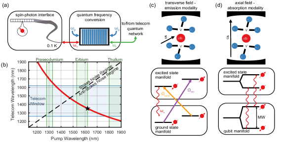
In QFC, an input quantum field is overlapped with a strong pump field (frequency ) inside of a nonlinear material, shifting the frequency of the input while otherwise preserving its quantum properties Kumar (1990). This is often performed as depicted in Figure 1(a), using difference(sum)-frequency generation in a material such as periodically poled lithium niobate (PPLN) to achieve frequency down(up)conversion between visible () and telecom () frequencies Dréau et al. (2018); Bock et al. (2018); Ikuta et al. (2018); Weber et al. (2019). While such nonlinear frequency conversion is routinely employed in classical applications for the production of coherent radiation at novel wavelengths or for detecting long-wavelength signals, in quantum applications, noise photons from spontaneous parametric downconversion (SPDC) and Raman scattering Pelc et al. (2010); Zaske et al. (2011) generated by the strong pump field (typically 100 mW-class) lower the resulting fidelity of the transduced quantum state Tchebotareva et al. (2019). At frequencies below the pump frequency , Stokes Raman and SPDC processes result in a broadband noise plateau, whereas at higher frequencies , the comparatively weaker anti-Stokes Raman signal typically tapers off for separations THz Pelc et al. (2011). This leads to two noise regimes — one lower-noise, anti-Stokes regime where , and one higher-noise, Stokes and SPDC-dominated regime where . Since is fixed by the choice of quantum memory, conservation of energy restricts the design of QFC schemes to only one degree of freedom. Moreover, the need for a strong pump laser introduces an additional engineering consideration due to availability of common gain materials. The resulting trade-space (Figure 1(b)) permits selection of a frequency conversion scheme based on the desired telecom wavelength, the noise requirements of the application, and the availability of pump laser amplifiers.
The negatively charged diamond SiV center is a promising candidate for the realization of quantum networks. Its electronic spin degree of freedom can store quantum information over millisecond timescales at dilution refrigerator temperatures Sukachev et al. (2017), and its optical transition exhibits nearly lifetime-limited spectral stability due to its inversion-symmetric electronic structure Sipahigil et al. (2014). This stability permits integration into nanophotonic crystal cavities which provide an efficient interface for spin-photon state transduction. For example, as shown in Figure 1(c), an overcoupled photonic crystal cavity enhances emission of the incorporated SiV into the desired optical mode. Under an applied transverse magnetic field, the SiV exhibits allowed transitions between spin states that can be driven to initialize the spin state via optical pumping, or to generate high quality, shaped single photons Knall et al. (2022). This “emission modality” is a resource for quantum networking or quantum photonic processing applications which benefit from sources of high-quality single photons Kok et al. (2007). Alternatively, an SiV can operate in an “absorption modality” when incorporated into a critically coupled photonic crystal cavity and placed in an axial magnetic field as shown in Figure 1(d) Nguyen et al. (2019a). This results in spin-dependent cavity reflectivity that can be used to generate entanglement with a reflected time-bin photonic qubit. The SiV’s 737 nm optical transition wavelength at which these protocols operate experiences strong loss in standard single-mode optical fiber ( dB/km), necessitating QFC to a low-loss telecom band. Examining the trade-space curve corresponding to the SiV in Fig. 1(b), we identify a point (black star) where a long-wavelength pump at 1623 nm facilitates conversion to the edge of the O-band at 1350 nm (typical loss dB/km in standard single-mode telecom fiber), permitting operation in the lower-noise anti-Stokes regime. This point maximizes within the parameter space in order to minimize pump-induced noise. See Supplemental Figure S1 for a similar analysis using other emerging quantum memories, as well as with multi-pump conversion schemes Hannegan et al. (2021).
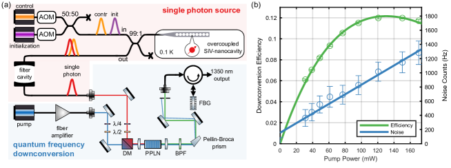
Figure 2(a) depicts our experimental setup for generating and converting single photons using a SiV center incorporated in an overcoupled photonic crystal cavity, following the approach used in Ref. Knall et al. (2022). A tapered optical fiber is coupled to the device to deliver optical control pulses, as well as to efficiently collect single photons. We apply optical control pulses to produce a shaped single photon output with a temporal width of 30 ns at a repetition rate of 670 kHz. A Fabry-Pérot filter removes residual optical excitation light from the emitted photons, resulting in a final single photon generation efficiency of within a 75 ns collection window.
Next, we convert these single photons to the telecom O-band using a custom-fabricated PPLN waveguide device (see Supplemental Material). Our input fields are a pump laser at 1623 nm amplified by a fiber amplifier and a 737 nm signal, either from a laser for QFC efficiency characterization, or from the output of our SiV emission setup for single-photon conversion experiments. An aspheric lens couples both fields into separate waveguide modes of the PPLN, where an on-chip wavelength division multiplexer (WDM) combines the two modes. The PPLN waveguide output is collimated by a second aspheric lens, and residual pump light is removed by a 25 nm bandpass filter followed by a Pellin-Broca prism with a pinhole after 40 cm of propagation length. Finally, the converted light is sent through a fine filter setup comprising a circulator and a 50-GHz-bandwidth fiber Bragg grating to remove broadband anti-Stokes Raman noise.
In the strong-pump limit, the total external conversion efficiency is dependent on the pump power in the waveguide and the length of the interaction region Roussev et al. (2004):
| (1) |
where is the combined efficiency of all optical components and filtering, is the maximum internal conversion efficiency of the PPLN, and is the normalized internal efficiency, which is determined by the nonlinear material, mode overlap, etc. We measure , limited by coupling losses between the crystal waveguide mode and optical fiber (32% total) and the fiber Bragg filter (59%). By measuring the maximum depletion of the input 737 nm signal, we estimate an internal efficiency . Sweeping the pump power (Fig. 2(b)) and fitting the 1350 nm output power to Eq. 1 shows a maximum conversion efficiency of , consistent with the losses described above. This conversion is maximized at an internal pump power of approximately 130 mW, which for our interaction length mm indicates a normalized internal efficiency W-1m-2. These figures are comparable to existing demonstrations Tchebotareva et al. (2019); Krutyanskiy et al. (2019); van Leent et al. (2020); Luo et al. (2022), and could be improved by further optimization of our coupling and device efficiency.
We probe the noise generated by the strong pump by measuring the setup output on superconducting nanowire single-photon detectors (SNSPDs) with zero 737 nm input power, plotted in Fig. 2(b) after correction for the SNSPD detection efficiency. The noise profile fits to a linear dependency of Hz/mW of noise photons generated by the pump, indicating anti-Stokes Raman scattering is the primary source. This noise reaches a count rate of kHz when the conversion efficiency is at its maximum. Due to the broadband nature of this pump-induced noise, a useful metric is the noise spectral density at maximum conversion Hz/GHz, which compares favorably to other systems designed for diamond defect centers Mann et al. (2023) and indicates the ultimate fidelity limits for a QFC system given optimal filtering.
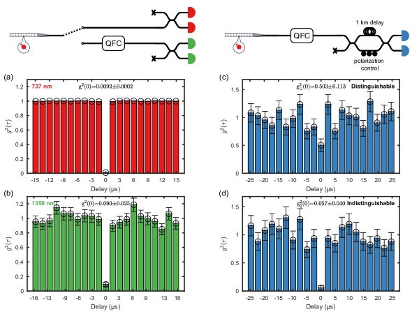
We characterize our QFC system’s ability to preserve quantum states by measuring the second-order correlations of the single photon output. First, we benchmark our single photon source at its native visible wavelength, finding good single photon character of without background or detector dark count subtraction (Fig. 3(a)). Next, we convert these single photons to the telecom O-band, then send them through a 0.1-km-long fiber network (69% efficient) between two buildings before detection on SNSPDs (29% efficient). During the single-photon conversion experiments, we measure a mean QFC efficiency of , attributing the additional loss and high variance compared to the classical case to polarization drift in the fibers between the SiV and our QFC setup. As a result, the signal-to-noise (SNR) ratio within our 75 ns gated time bins is . For the converted photons, we measure , again without background or detector dark count subtraction (Fig. 3(b)), indicating good preservation of quantum properties through QFC.
The quantum properties of our converted photons can be further probed via Hong-Ou-Mandel interference between subsequent SiV emissions, using a 1 km delay line as shown in Figure 3. A polarization controller in the short arm of the resultant interferometer permits us to adjust the relative polarizations between the two arms and compare between the distinguishable case, where the photons arriving from both arms at the final beamsplitter are cross-polarized (Fig. 3(c)), and the indistinguishable case, where the photons arriving at the final beamsplitter are co-polarized (Fig. 3(d)). We measure a HOM interference visibility . Note that a comparison to the instrinsic indistinguishability pre-conversion is not possible due to the difficulty in retaining visible photons over the requisite km-scale delay line.
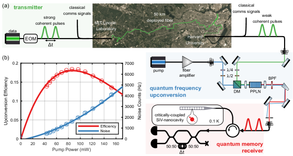
We next demonstrate that our scheme is compatible with absorption-based quantum memory protocols by performing frequency upconversion on a telecom-wavelength qubit. Figure 4(a) depicts our experimental setup for generating telecom time-bin photonic qubits, upconverting them to match the SiV’s visible transition, and generating spin-photon entanglement. For this experiment, we use an SiV in a critically coupled photonic crystal cavity Stas et al. (2022) and an axial magnetic field, resulting in spin-dependent cavity reflectivity that can be used to generate entanglement with a reflected time-bin photonic qubit.
We use a 1350 nm laser to generate coherent time-bin pulses with a full-width at half-maximum of 45 ns and separated by 144.5 ns. These pulses are generated at MIT Lincoln Laboratory in Lexington, MA, 15.4 km away from the QFC receiver at Harvard University in Cambridge, MA. A 50 km deployed fiber link connects the two sites and attenuates the pulses by 40.8 dB such that they ultimately arrive at the SiV device as qubits with mean photon number per pulse. This channel also imparts noise associated with deployed fiber communications, including polarization drift, timing drift, and Doppler shifts. To coordinate between the two sites, we co-propagate a 1550 nm clock signal which synchronizes the experiment between the two sites, as well as a periodic 1350 nm reference signal to correct for polarization drifts over the deployed fiber and to serve as a reference for any drift in the photonic qubit’s optical frequency. Details about the link as well as our classical communications protocol for synchronization and stabilization can be found in Ref. Ber .
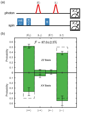
We modify our QFC setup from Fig. 2(a) to upconvert light from 1350 nm to 737 nm via sum-frequency generation using an identically-fabricated PPLN device. Compared to the previous setup, we replace the lenses and filters to be wavelength-appropriate, and propagate the optical fields in reverse through the PPLN so that the on-chip WDM is at the output rather than the input. Importantly, the increased spectral separation between the pump and converted wavelength for upconversion relaxes our filtering requirements, such that the converted light is only filtered by a 13-nm-bandwidth bandpass filter and a prism, without any fine filtering stage. As shown in Figure 4(b), we are thus able to attain an increased conversion efficiency of while maintaining a low noise count rate of kHz. We note that here, the noise profile fits well to a quadratic power dependency, suggesting these noise counts are dominated by upconversion of anti-Stokes photons rather than direct Raman noise Pelc et al. (2011). The output of the conversion setup is sent through a fiber-optic circulator and delivered via a tapered fiber to the SiV-cavity, where light is transmitted or reflected depending on the SiV spin state. Reflected light is routed to a time-delay interferometer (TDI) that measures the photonic qubit using avalanche photodiodes. Using this system and the pulse sequence shown in Figure 5(a), we generate the spin-photon entangled state conditioned on successful detection of a reflected photon. Here, and denote the presence of a photon in an early or late time bin respectively. We characterize this entanglement by measuring the photon and the spin in the joint - and -bases. Figure 5(b) shows the retrieved spin-photon correlations, limited primarily by residual reflectivity of the state (see Supplemental Material). Following Nguyen et al. (2019b), we use these correlations to calculate an entanglement-mediated state transfer fidelity of %. This result constitutes a heralded state transfer that reveals no information about the absorbed state, providing a key resource for quantum repeaters and other quantum networking protocols.
Taken together, these experiments demonstrate bi-directional quantum state transfer between a diamond quantum memory and telecom photons facilitated by quantum frequency conversion. In particular, the SiV’s 737 nm transition wavelength and our choice of conversion between the telecom O-band enabled the use of a long-wavelength pump, reducing the noise induced by the conversion process. Our heralded state transfer from a telecom photon to a diamond memory, incorporating classical telecommunication signals for timing synchronization and stabilization over deployed fiber, highlights the compatibility of the SiV platform with telecommunication infrastructure. This work can be extended and improved along several directions. The conversion efficiency was limited by coupling losses and non-unity internal conversion efficiency, and could be improved by further device optimization to realize up to Yao et al. (2020). Our downconversion demonstration utilized a broad filter over the SiV’s lifetime limited linewidth; using a narrower final filter thus offers a clear avenue for further SNR improvement. While our state transfer fidelity was limited by the finite cooperativity of the device used here (max ), other works have shown higher cooperativities , enabling higher fidelities Bhaskar et al. (2020).
The ability to transduce single photon quantum states between visible and telecom wavelengths with high fidelity has implications across quantum information science applications. Single telecom photons are an important resource for photonic quantum computing; replacing current SPDC-based sources with single telecom photons would improve processing efficiency and reduce errors from multi-photon events Duan and Kimble (2004); Knall et al. (2022). Furthermore, our system can be used for generating multiphoton entangled states when interfaced with a second cavity-coupled SiV Bhaskar et al. (2020). When used as an input to a photonic processor, such cluster states can dramatically improve the efficiency and fidelity of photonic quantum computers Lindner and Rudolph (2009). When combined with access to nuclear memories Stas et al. (2022) and improved nanophotonic devices, these results offer a path towards more general deployed quantum networking. The high-bandwidth nature of our conversion system (see Supplemental Material) enables bridging of the frequency difference between individual SiVs due to the natural inhomogeneous distribution Yu et al. (2015); Sutula et al. (2022); Stolk et al. (2022), and provides an avenue for taking advantage of the built-in spectral multiplexing of solid-state memories Bersin et al. (2019). This approach also allows for interfacing SiVs with other quantum information platforms such as neutral atoms van Leent et al. (2022), trapped ions Bock et al. (2018); Krutyanskiy et al. (2023), or other color centers in diamond Pompili et al. (2021); Ruf et al. (2021), where performing frequency conversion to a common wavelength would facilitate photonic-mediated entanglement generation between these systems. This could enable quantum networks comprising diverse physical qubits, where different applications including computing, communication or sensing could be performed by physical systems best tailored to the task.
References
- Gottesman et al. (2012) Daniel Gottesman, Thomas Jennewein, and Sarah Croke, “Longer-baseline telescopes using quantum repeaters,” Phys. Rev. Lett. 109, 070503 (2012).
- Khabiboulline et al. (2019) E. T. Khabiboulline, J. Borregaard, K. De Greve, and M. D. Lukin, “Quantum-assisted telescope arrays,” Phys. Rev. A 100, 022316 (2019).
- Xu et al. (2020) Feihu Xu, Xiongfeng Ma, Qiang Zhang, Hoi-Kwong Lo, and Jian-Wei Pan, “Secure quantum key distribution with realistic devices,” Rev. Mod. Phys. 92, 025002 (2020).
- Kimble (2008) H. J. Kimble, “The quantum internet,” Nature 453, 1023–1030 (2008).
- Lindner and Rudolph (2009) Netanel H. Lindner and Terry Rudolph, “Proposal for pulsed on-demand sources of photonic cluster state strings,” Phys. Rev. Lett. 103, 113602 (2009).
- Briegel et al. (1998) H.-J. Briegel, W. Dür, J. I. Cirac, and P. Zoller, “Quantum repeaters: The role of imperfect local operations in quantum communication,” Phys. Rev. Lett. 81, 5932–5935 (1998).
- Munro et al. (2010) W. J. Munro, K. A. Harrison, A. M. Stephens, S. J. Devitt, and Kae Nemoto, “From quantum multiplexing to high-performance quantum networking,” Nat. Photonics 4, 792–796 (2010).
- Hermans et al. (2022) S. L. N. Hermans, M. Pompili, H. K. C. Beukers, S. Baier, J. Borregaard, and R. Hanson, “Qubit teleportation between non-neighbouring nodes in a quantum network,” Nature 605, 663–668 (2022).
- Schwartz et al. (2016) I. Schwartz, D. Cogan, E. R. Schmidgall, Y. Don, L. Gantz, O. Kenneth, N. H. Lindner, and D. Gershoni, “Deterministic generation of a cluster state of entangled photons,” Science 354, 434–437 (2016).
- Kumar (1990) Prem Kumar, “Quantum frequency conversion,” Opt. Lett. 15, 1476–1478 (1990).
- Dréau et al. (2018) Anaïs Dréau, Anna Tchebotareva, Aboubakr El Mahdaoui, Cristian Bonato, and Ronald Hanson, “Quantum frequency conversion of single photons from a nitrogen-vacancy center in diamond to telecommunication wavelengths,” Phys. Rev. Applied 9, 064031 (2018).
- Bock et al. (2018) Matthias Bock, Pascal Eich, Stephan Kucera, Matthias Kreis, Andreas Lenhard, Christoph Becher, and Jürgen Eschner, “High-fidelity entanglement between a trapped ion and a telecom photon via quantum frequency conversion,” Nature Communications 9, 1998 (2018).
- Ikuta et al. (2018) Rikizo Ikuta, Toshiki Kobayashi, Tetsuo Kawakami, Shigehito Miki, Masahiro Yabuno, Taro Yamashita, Hirotaka Terai, Masato Koashi, Tetsuya Mukai, Takashi Yamamoto, and Nobuyuki Imoto, “Polarization insensitive frequency conversion for an atom-photon entanglement distribution via a telecom network,” Nature Communications 9, 1997 (2018).
- Weber et al. (2019) Jonas H. Weber, Benjamin Kambs, Jan Kettler, Simon Kern, Julian Maisch, Hüseyin Vural, Michael Jetter, Simone L. Portalupi, Christoph Becher, and Peter Michler, “Two-photon interference in the telecom c-band after frequency conversion of photons from remote quantum emitters,” Nature Nanotechnology 14, 23–26 (2019).
- Pelc et al. (2010) J. S. Pelc, C. Langrock, Q. Zhang, and M. M. Fejer, “Influence of domain disorder on parametric noise in quasi-phase-matched quantum frequency converters,” Opt. Lett. 35, 2804–2806 (2010).
- Zaske et al. (2011) Sebastian Zaske, Andreas Lenhard, and Christoph Becher, “Efficient frequency downconversion at the single photon level from the red spectral range to the telecommunications c-band,” Opt. Express 19, 12825–12836 (2011).
- Tchebotareva et al. (2019) Anna Tchebotareva, Sophie L. N. Hermans, Peter C. Humphreys, Dirk Voigt, Peter J. Harmsma, Lun K. Cheng, Ad L. Verlaan, Niels Dijkhuizen, Wim de Jong, Anaïs Dréau, and Ronald Hanson, “Entanglement between a diamond spin qubit and a photonic time-bin qubit at telecom wavelength,” Phys. Rev. Lett. 123, 063601 (2019).
- Pelc et al. (2011) J. S. Pelc, L. Ma, C. R. Phillips, Q. Zhang, C. Langrock, O. Slattery, X. Tang, and M. M. Fejer, “Long-wavelength-pumped upconversion single-photon detector at 1550 nm: performance and noise analysis,” Opt. Express 19, 21445–21456 (2011).
- Sukachev et al. (2017) D. D. Sukachev, A. Sipahigil, C. T. Nguyen, M. K. Bhaskar, R. E. Evans, F. Jelezko, and M. D. Lukin, “Silicon-vacancy spin qubit in diamond: A quantum memory exceeding 10 ms with single-shot state readout,” Phys. Rev. Lett. 119, 223602 (2017).
- Sipahigil et al. (2014) A. Sipahigil, K. D. Jahnke, L. J. Rogers, T. Teraji, J. Isoya, A. S. Zibrov, F. Jelezko, and M. D. Lukin, “Indistinguishable photons from separated silicon-vacancy centers in diamond,” Phys. Rev. Lett. 113, 113602 (2014).
- Knall et al. (2022) E. N. Knall, C. M. Knaut, R. Bekenstein, D. R. Assumpcao, P. L. Stroganov, W. Gong, Y. Q. Huan, P.-J. Stas, B. Machielse, M. Chalupnik, D. Levonian, A. Suleymanzade, R. Riedinger, H. Park, M. Lončar, M. K. Bhaskar, and M. D. Lukin, “Efficient source of shaped single photons based on an integrated diamond nanophotonic system,” Phys. Rev. Lett. 129, 053603 (2022).
- Kok et al. (2007) Pieter Kok, W. J. Munro, Kae Nemoto, T. C. Ralph, Jonathan P. Dowling, and G. J. Milburn, “Linear optical quantum computing with photonic qubits,” Rev. Mod. Phys. 79, 135–174 (2007).
- Nguyen et al. (2019a) C. T. Nguyen, D. D. Sukachev, M. K. Bhaskar, B. Machielse, D. S. Levonian, E. N. Knall, P. Stroganov, R. Riedinger, H. Park, M. Lončar, and M. D. Lukin, “Quantum network nodes based on diamond qubits with an efficient nanophotonic interface,” Phys. Rev. Lett. 123, 183602 (2019a).
- Hannegan et al. (2021) J. Hannegan, U. Saha, J. D. Siverns, J. Cassell, E. Waks, and Q. Quraishi, “C-band single photons from a trapped ion via two-stage frequency conversion,” Applied Physics Letters 119, 084001 (2021).
- Roussev et al. (2004) Rostislav V. Roussev, Carsten Langrock, Jonathan R. Kurz, and M. M. Fejer, “Periodically poled lithium niobate waveguide sum-frequency generator for efficient single-photon detection at communication wavelengths,” Opt. Lett. 29, 1518–1520 (2004).
- Krutyanskiy et al. (2019) V. Krutyanskiy, M. Meraner, J. Schupp, V. Krcmarsky, H. Hainzer, and B. P. Lanyon, “Light-matter entanglement over 50 km of optical fibre,” npj Quantum Information 5, 72 (2019).
- van Leent et al. (2020) Tim van Leent, Matthias Bock, Robert Garthoff, Kai Redeker, Wei Zhang, Tobias Bauer, Wenjamin Rosenfeld, Christoph Becher, and Harald Weinfurter, “Long-distance distribution of atom-photon entanglement at telecom wavelength,” Phys. Rev. Lett. 124, 010510 (2020).
- Luo et al. (2022) Xi-Yu Luo, Yong Yu, Jian-Long Liu, Ming-Yang Zheng, Chao-Yang Wang, Bin Wang, Jun Li, Xiao Jiang, Xiu-Ping Xie, Qiang Zhang, Xiao-Hui Bao, and Jian-Wei Pan, “Postselected entanglement between two atomic ensembles separated by 12.5 km,” Phys. Rev. Lett. 129, 050503 (2022).
- Mann et al. (2023) Felix Mann, Helen M. Chrzanowski, Felipe Gewers, Marlon Placke, and Sven Ramelow, “Low-noise quantum frequency conversion in a monolithic bulk ppktp cavity,” (2023), arXiv:2304.13459 .
- Stas et al. (2022) P.-J. Stas, Y. Q. Huan, B. Machielse, E. N. Knall, A. Suleymanzade, B. Pingault, M. Sutula, S. W. Ding, C. M. Knaut, D. R. Assumpcao, Y.-C. Wei, M. K. Bhaskar, R. Riedinger, D. D. Sukachev, H. Park, M. Lončar, D. S. Levonian, and M. D. Lukin, “Robust multi-qubit quantum network node with integrated error detection,” Science 378, 557–560 (2022).
- (31) ”Development of a Boston-area 50 km fiber quantum network testbed”, in preparation.
- Nguyen et al. (2019b) C. T. Nguyen, D. D. Sukachev, M. K. Bhaskar, B. Machielse, D. S. Levonian, E. N. Knall, P. Stroganov, C. Chia, M. J. Burek, R. Riedinger, H. Park, M. Lončar, and M. D. Lukin, “An integrated nanophotonic quantum register based on silicon-vacancy spins in diamond,” Phys. Rev. B 100, 165428 (2019b).
- Yao et al. (2020) Ni Yao, Quan Yao, Xiu-Ping Xie, Yang Liu, Peizhen Xu, Wei Fang, Ming-Yang Zheng, Jingyun Fan, Qiang Zhang, Limin Tong, and Jian-Wei Pan, “Optimizing up-conversion single-photon detectors for quantum key distribution,” Opt. Express 28, 25123–25133 (2020).
- Bhaskar et al. (2020) M. K. Bhaskar, R. Riedinger, B. Machielse, D. S. Levonian, C. T. Nguyen, E. N. Knall, H. Park, D. Englund, M. Lončar, D. D. Sukachev, and M. D. Lukin, “Experimental demonstration of memory-enhanced quantum communication,” Nature 580, 60–64 (2020).
- Duan and Kimble (2004) L.-M. Duan and H. J. Kimble, “Scalable photonic quantum computation through cavity-assisted interactions,” Phys. Rev. Lett. 92, 127902 (2004).
- Yu et al. (2015) Leo Yu, Chandra M. Natarajan, Tomoyuki Horikiri, Carsten Langrock, Jason S. Pelc, Michael G. Tanner, Eisuke Abe, Sebastian Maier, Christian Schneider, Sven Höfling, Martin Kamp, Robert H. Hadfield, Martin M. Fejer, and Yoshihisa Yamamoto, “Two-photon interference at telecom wavelengths for time-bin-encoded single photons from quantum-dot spin qubits,” Nature Communications 6, 8955 (2015).
- Sutula et al. (2022) Madison Sutula, Ian Christen, Eric Bersin, Michael P. Walsh, Kevin C. Chen, Justin Mallek, Alexander Melville, Michael Titze, Edward S. Bielejec, Scott Hamilton, Danielle Braje, P. Benjamin Dixon, and Dirk R. Englund, “Large-scale optical characterization of solid-state quantum emitters,” (2022), arXiv:2210.13643 .
- Stolk et al. (2022) A.J. Stolk, K.L. van der Enden, M.-C. Roehsner, A. Teepe, S.O.F. Faes, C.E. Bradley, S. Cadot, J. van Rantwijk, I. te Raa, R.A.J. Hagen, A.L. Verlaan, J.J.B. Biemond, A. Khorev, R. Vollmer, M. Markham, A.M. Edmonds, J.P.J. Morits, T.H.T. Taminiau, E.J. van Zwet, and R. Hanson, “Telecom-band quantum interference of frequency-converted photons from remote detuned nv centers,” PRX Quantum 3, 020359 (2022).
- Bersin et al. (2019) Eric Bersin, Michael Walsh, Sara L. Mouradian, Matthew E. Trusheim, Tim Schröder, and Dirk Englund, “Individual control and readout of qubits in a sub-diffraction volume,” npj Quantum Inf. 5, 38 (2019).
- van Leent et al. (2022) Tim van Leent, Matthias Bock, Florian Fertig, Robert Garthoff, Sebastian Eppelt, Yiru Zhou, Pooja Malik, Matthias Seubert, Tobias Bauer, Wenjamin Rosenfeld, Wei Zhang, Christoph Becher, and Harald Weinfurter, “Entangling single atoms over 33 km telecom fibre,” Nature 607, 69–73 (2022).
- Krutyanskiy et al. (2023) V. Krutyanskiy, M. Galli, V. Krcmarsky, S. Baier, D. A. Fioretto, Y. Pu, A. Mazloom, P. Sekatski, M. Canteri, M. Teller, J. Schupp, J. Bate, M. Meraner, N. Sangouard, B. P. Lanyon, and T. E. Northup, “Entanglement of trapped-ion qubits separated by 230 meters,” Phys. Rev. Lett. 130, 050803 (2023).
- Pompili et al. (2021) M. Pompili, S. L. N. Hermans, S. Baier, H. K. C. Beukers, P. C. Humphreys, R. N. Schouten, R. F. L. Vermeulen, M. J. Tiggelman, L. dos Santos Martins, B. Dirkse, S. Wehner, and R. Hanson, “Realization of a multinode quantum network of remote solid-state qubits,” Science 372, 259–264 (2021).
- Ruf et al. (2021) Maximilian Ruf, Noel H. Wan, Hyeongrak Choi, Dirk Englund, and Ronald Hanson, “Quantum networks based on color centers in diamond,” Journal of Applied Physics 130, 070901 (2021).
- Esfandyarpour et al. (2018) Vahid Esfandyarpour, Carsten Langrock, and Martin Fejer, “Cascaded downconversion interface to convert single-photon-level signals at 650 nm to the telecom band,” Opt. Lett. 43, 5655–5658 (2018).
- Lu et al. (2021) Xiyuan Lu, Gregory Moille, Ashutosh Rao, and Kartik Srinivasan, “Proposal for noise-free visible-telecom quantum frequency conversion through third-order sum and difference frequency generation,” Opt. Lett. 46, 222–225 (2021).
- Trusheim et al. (2020) Matthew E. Trusheim, Benjamin Pingault, Noel H. Wan, Mustafa Gündoğan, Lorenzo De Santis, Romain Debroux, Dorian Gangloff, Carola Purser, Kevin C. Chen, Michael Walsh, Joshua J. Rose, Jonas N. Becker, Benjamin Lienhard, Eric Bersin, Ioannis Paradeisanos, Gang Wang, Dominika Lyzwa, Alejandro R-P. Montblanch, Girish Malladi, Hassaram Bakhru, Andrea C. Ferrari, Ian A. Walmsley, Mete Atatüre, and Dirk Englund, “Transform-limited photons from a coherent tin-vacancy spin in diamond,” Phys. Rev. Lett. 124, 023602 (2020).
- Bortz et al. (1994) M.L. Bortz, S.J. Field, M.M. Fejer, D.W. Nam, R.G. Waarts, and D.F. Welch, “Noncritical quasi-phase-matched second harmonic generation in an annealed proton-exchanged LiNbO3 waveguide,” IEEE Journal of Quantum Electronics 30, 2953–2960 (1994).
Acknowledgements.
This material is based upon work supported by the National Reconnaissance Office and the Under Secretary of Defense for Research and Engineering under Air Force Contract No. FA8702-15-D-0001. Any opinions, findings, conclusions or recommendations expressed in this material are those of the authors and do not necessarily reflect the views of the National Reconnaissance Office or the Under Secretary of Defense for Research and Engineering. © 2023 Massachusetts Institute of Technology. Delivered to the U.S. Government with Unlimited Rights, as defined in DFARS Part 252.227-7013 or 7014 (Feb 2014). Notwithstanding any copyright notice, U.S. Government rights in this work are defined by DFARS 252.227-7013 or DFARS 252.227-7014 as detailed above. Use of this work other than as specifically authorized by the U.S. Government may violate any copyrights that exist in this work. We thank Catherine Lee for helpful discussions. This work was supported by the National Science Foundation (NSF, Grant No. PHY-2012023), NSF EFRI ACQUIRE (Grant No. 5710004174), NSF QuIC-TAQS (Grant No. OMA-2137723), Center for Ultracold Atoms (Grant No. PHY-1734011), Department of Energy (DoE, Grant No. DESC0020115), AFOSR MURI (Grants No. FA9550171002 and No. FA95501610323), and Center for Quantum Networks (Grant No. EEC-1941583). Devices were fabricated at the Harvard Center for Nanoscale Systems, NSF award no. 1541959. E.B. and M.S. acknowledge funding from a NASA Space Technology Research Fellowship. Y.Q.H. acknowledges support from the Agency for Science, Technology and Research (A*STAR) National Science Scholarship. D.A., E.N.K., and B.M. acknowledge support by the NSF Graduate Research Fellowship under Grant No. DGE1745303. M.Y. acknowledges funding from the Department of Defence (DoD) through the National Defense Science and Engineering Graduate (NDSEG) Fellowship Program. We thank Planet.com for allowing us to take custom satellite imagery.Supplemental Material for “Telecom networking with a diamond quantum memory”
S1 Frequency Conversion Tradespace
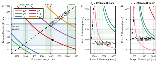
As discussed in the main text, quantum frequency conversion poses a tradespace where loss, noise, and availability of laser gain material must be balanced. Figure 1(b) depicts this for the SiV; Figure S1(a) repeats this figure, adding curves for other emerging quantum memories. This tradespace assumes a single -based frequency conversion step; an alternative approach is to use either a higher order -based process where , or multiple -based conversion stages, in either case using two pumps at frequencies and Esfandyarpour et al. (2018); Hannegan et al. (2021). This is attractive for systems that need to span large frequency differences, as it can permit each individual step to operate in the low-noise anti-Stokes regime. Here, while most quantum systems can operate in the anti-Stokes regime, a greater challenge is the dearth of common gain materials for the requisite pump laser wavelengths. Figures S1(b)–(c) plot the parameter space for these “two-step” conversions. Due to the larger solution space for this approach, we fix the final converted wavelength to either 1310 nm (Fig. S1(b)) or 1550 nm (Fig. S1(c)) corresponding to the telecom O- and C-bands respectively. We note that these telecom bands are nm wide each, giving some flexibility in the vicinity of these curves. Importantly, this figure omits consideration of the challenges that arise for large separations between and , such as engineering strong overlap between waveguide modes when one wavelength is much larger than the other, which can lead to undesired multimode behavior of the shorter (though this can also be used intentionally Lu et al. (2021)).
S2 Periodically Poled Lithium Niobate (PPLN) Device
We fabricate a device starting from bulk lithium niobate to facilitate QFC, using periodic poling to achieve quasi-phasematching (QPM) and incorporating waveguides to realize efficient spatial overlap of the participating optical modes. As shown in the schematic in Figure S2(a), the length of the reverse-proton-exchange (RPE) periodically poled lithium niobate (PPLN) waveguide chip, containing 32 individual QFC devices, was 52 mm. Each QFC device comprised an on-chip directional coupler (Fig. S2(b)) with a waveguide-to-waveguide separation of 10 µm to efficiently combine the 1623 nm pump and the 737 nm signal, and a 35-mm-long QPM section with a poling period of 14.5 um for Type-0 difference-frequency generation between the 737-nm signal and the 1623-nm pump. The waveguide width in the coupler section was 5 µm, while it was 8 µm in the QPM section, optimized for noncritical operation Bortz et al. (1994).
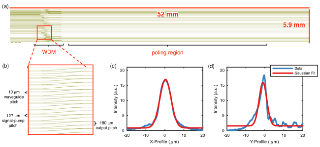
To maximize the conversion and coupling efficiency, we designed the two 127-µm-separated input ports to each device (pump and signal) to only support the respective lowest-order waveguide modes and have mode-field diameters close to those encountered in single-mode fiber. Imaging the output mode of these waveguide devices at 1350 nm, we find that the waveguide mode is fairly Gaussian in the horizontal direction (x-direction), with a 1/ mode field diameter (MFD) of 11.8 µm (Fig. S2(c)). However, we observe an asymmetry in the vertical (y-direction) extent of the mode with an 8.2 µm MFD (Fig. S2(d)), decreasing coupling efficiency between this mode and the Gaussian mode of optical fiber. An antireflection coating was also applied (Forreal Spectrum) to each end facet to improve input coupling efficiency. While we operated these device using free-space coupling, low-loss fiber coupling has previously been demonstrated and is expected to introduce a 0.5 dB coupling loss for both pump and signal, which could improve the external conversion efficiency up to Yao et al. (2020).
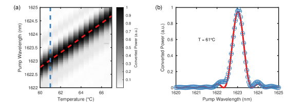
We characterized the transfer function of one waveguide on the device by measuring the power of converted light as a function of chip temperature and pump power, shown in Figure S3(a). As we did not realign the chip in between temperature setpoints, the results have been normalized for each temperature setting to account for differences in coupling efficiency. We find a 0.28 nm/∘C shift in the phase-matched pump wavelength as a function of chip temperature (red dashed line). A cross-section of this transfer function is shown in Figure S3(b), taken at the temperature (C) where our desired conversion process was optimally phase-matched. A fit to the expected sinc function shows a slight asymmetry in the transfer function, indicating minor geometrical inhomogeneities of the waveguide along its length that locally modify the dispersion; however, the function largely matches theoretical expectations, indicating the device is well-suited for efficient frequency conversion. The experiments described in the main text were performed on a waveguide which had an optimal phase-matching temperature of 55.5∘C, which we achieved by operating the chip inside of a temperature-controlled housing (HC Photonics).
S3 State Absorption Experiment Details
S3.1 Deployed Fiber Network
For the state absorption experiment, our transmitter (Alice) is stationed at MIT Lincoln Laboratory in Lexington, MA. Our memory-enabled receiver (Bob) is stationed at Harvard campus in Cambridge, MA; this node is connected by 50 km of fiber to Alice (40.8 dB at 1350 nm). A third network node (Charlie) used only as a passive pass-through in this work but available for future demonstrations is located at MIT campus in Cambridge, MA. A 43 km strand of single-mode telecom fiber (24.1 dB at 1350 nm) connects Alice to Charlie, and 7 km of fiber connects Charlie to Bob (19.7 dB at 1350 nm), forming an all-to-all 3-node network. We note that these losses are primarily due to splices in this commercial fiber link rather than the expected inherent exponential propagation loss. For extended details on this link, see Ref. Ber .
S3.2 Transmitter
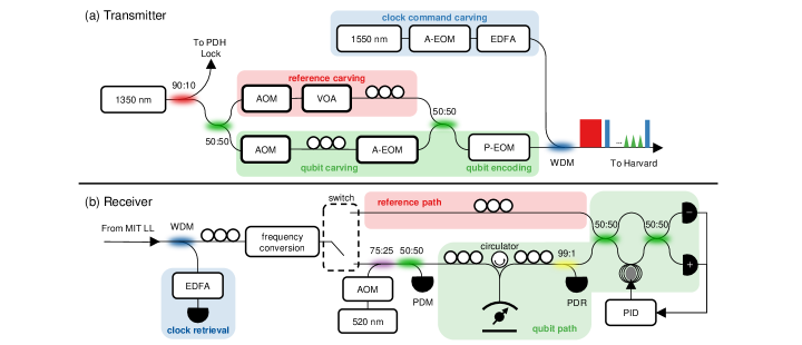
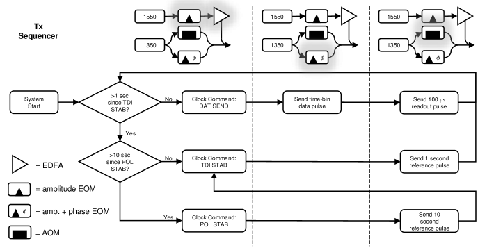
The overall optical setup used for generating the quantum and classical signals sent from Alice to Bob is shown in Figure S4(a). Details about the classical signals for performing timing synchronization, polarization drift correction, and frequency transfer across the link can be found in Ref. Ber . Our photonic qubits are generated by attenuated coherent laser pulses. A 1350 nm ECDL laser (Toptica) is locked to an ultra low expansion Fabry-Pérot cavity (Stable Laser Systems) to ensure narrow linewidth. Light from this laser is split out, passed through an accousto-optic modulator (AOM, Brimrose) for power and frequency control, then passed through an amplitude electro-optic modulator (EOM, EOSPACE, Inc.) which carves pulses to form time bin qubits. Each pulse is a Lorentzian with full width at half maximum ns, and the time bins are spaced 144.5 ns apart. After pulse carving, a phase EOM encodes phases on each time bin, achieved by applying a step-like voltage pattern to the EOM. The resultant output is combined with our synchronization and reference signals before being sent across the network. All of the opto-electronic devices for the transmitter are controlled using a single HD Arbitrary Waveform Generator (HD-AWG, Zurich Instruments). The full experimental sequence for this transmitter AWG is shown in Figure S5.
S3.3 Receiver: Optics and Sequencing
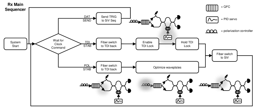
The overall optical setup used at the receiver for processing incoming clock, reference, and data signals is shown in Figure S4(b). The receiver makes use of two AWG sequencers: one “Main Sequencer” that processes classical information arriving over the fiber network and dictates the progress of the overall experimental sequence (Fig. S6; for detailed operation, see Ref. Ber ), and one “SiV Sequencer” that is triggered by the Main Sequencer and is responsible for SiV control (see below). As stated above, Alice’s transmitter coordinates between periods of data transmission and stabilization by sending clock commands to Bob, where they are picked off, amplified, detected, digitized, and processed by Bob’s Main Sequencer according to the flow chart shown in Fig. S6. During data periods, a MEMS switch (Agiltron) routes incoming qubits along the “qubit path” towards the memory. During stabilization periods, the MEMS switch bypasses the memory and routes the incoming high intensity reference signal directly to the TDI via the “reference path” to avoid fridge heating and excessive radiation on the SiV.
S3.4 Receiver: Diamond network node
S3.4.1 Optics
Details about the SiV-cavity system, including fabrication techniques, cavity parameters, and spin properties can be found in Ref. Stas et al. (2022), which employed the same device and SiV defect as the experiments discussed here, though on a separate cool-down of the system, such that the precise values of the cavity QED parameters, coupling efficiencies, etc. may slightly differ. As shown in Fig. S4(b), the optical path for our qubits after the MEMS switch comprises a 75:25 splitter for incorporating 520 nm repump light (with qubits following the 75% path), a 50:50 splitter for measuring incident and reflected powers, various polarization controllers, a fiber-optic circulator (Ascentta), the SiV-cavity memory, and a TDI for qubit measurement. We measure 9% transmission efficiency through the fiber-optic components (MEMS switch, splitters, and circulator), and estimate the efficiency of the SiV-cavity reflectivity (including losses from the adiabatic tapered fiber coupling) to be 15%. Combined with our frequency conversion efficiency of 19%, this yields an overall efficiency to detect photons arriving at the receiver node of 2.6.
S3.4.2 Electronics
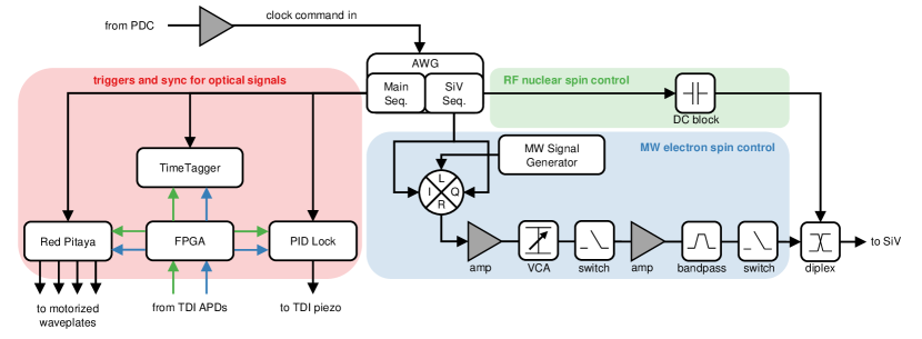
Figure S7 shows the electronics used to control the SiV spin and all other necessary components in the receiver. The components of this figure related to SiV spin control and detection of reflected photons has been adapted from Ref. Stas et al. (2022), which contains additional information about the parameters used for these electronics. Electron spin control is performed by the microwave (MW) electronics shown in the blue region of Fig. S7, where an radio-frequency (RF) output of the AWG is mixed with a local oscillator, then amplified, filter, and switched before being sent to the dilution refrigerator, where gold striplines facilitate spin driving. Nuclear spin control is achieved by direct driving from the AWG’s RF output (green region of Fig. S7).
The red region of Fig. S7 shows circuitry related to the optical signals of the experiment. Detected TTL signals from our avalanche photodiodes (APDs) are sent to a custom-built FPGA which, which simply serves as a buffer to split the signal to three other systems: the AWG for state initialization logic, a TimeTagger (Swabian Instruments) for photonic qubit heralding and SiV state readout, and a custom-built PID Lock box that generates an error signal from the difference in APD counts. This PID box also produces a buffered voltage proportional to the total count rate, which is sent to a Red Pitaya; this enables the Red Pitaya to control the automated waveplates on our conversion setup to maximize system throughput, thus correcting for polarization drifts over the deployed fiber. Finally, the activity of these systems is controlled by digital lines from the AWG which trigger these various protocols and serve as a timing reference for the TimeTagger. Not shown here, digital signals from the AWG are also used to control the MEMS switch and AOM for our 520 nm repump laser as shown in Fig. S4(b).
S3.4.3 Spin-Cavity System
Both our spin readout and our spin-photon gate rely on high reflectivity contrast between the bright and dark SiV spin states. Figure S8(a) shows a free-running time trace of reflected counts off of the SiV-nanocavity system under weak illumination. Distinct jumps between periods of high and low reflectivity are observed, corresponding to quantum jumps in the SiV spin state. This behavior enables us to perform high-fidelity, single-shot, non-demolition spin readout under pulsed illumination of the system. Figure S8(b) also shows an example histogram of the counts retrieved during such 1 ms readout bins. For this dataset, the SiV was initialized into before readout. Here, the data have been separated out into two categories (green and blue) based on the clear bimodal behavior, and each of the two resultant distributions normalized and fit with a Poisson probability distribution. Processing the data in this way, where the state of the SiV is purposefully placed into a superposition before readout, permits us to isolate our determination of the readout fidelity from any infidelities in state initialization. For the data shown here, the retreived mean counts of and indicate that by thresholding at 15 counts, single-shot readout can in principle be performed with an error probability of . Note that despite the high readout fidelity, the infidelity of our spin-photon gate will still be limited by the contrast .

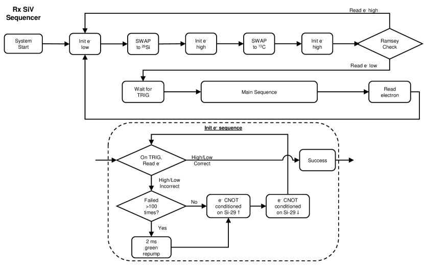
Due to spectral diffusion of the SiV transition, this contrast can drift over time, diminishing the fidelity of both our readout and our spin-photon gate. Before every string of photonic qubits, we thus perform an SiV initialization sequence that verifies good contrast between the bright and dark states, only moving forward once this check has cleared. The full sequence for SiV spin initialization is shown in Figure S9. For this check, we read the state of the spin using a 100 µs pulse of readout light; if we are attempting to initializing into (), this check only passes if we measure fewer (more) than 2 (20) photons. Otherwise, we attempt to reinitialize the spin, following the sequence depicted in Fig. S9. Furthermore, in order to ensure high contrast for the incoming qubits themselves, all spin readout for this initialization sequence is performed using upconverted reference light from Alice, rather than using a laser local to Bob. As such, all readout — both during the main experimental sequence and during initialization — is timed based on the incoming clock commands from Alice.
S3.4.4 Spin control fidelity
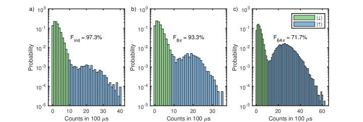
We characterize our control of the SiV spin by performing a variety of gate sequences that, when error-free, should conclude with the SiV in . First, we perform the initialization sequence described above, using 100 µs pulses for initialization and readout. We find that this sequence initializes the spin with fidelity (Fig. S10(a)). Next, we check the fidelity of our microwave gates by performing a modified version of the XYN sequence used for the main experiment, where the initial and concluding gates are removed to reduce sensitivity to external noise. The results of this check are shown in Fig. S10(b) for XY8 and Fig. S10(c) for XY64. The degradation in fidelity here indicates a gate fidelity of 99.5% per \textpi-pulse, which provides an upper limit on the fidelity we can expect to achieve for longer pulse sequences.
