3D-Carbon: An Analytical Carbon Modeling Tool
for 3D and 2.5D Integrated Circuits
Abstract
Environmental sustainability, driven by concerns about climate change, resource depletion, and pollution at local and global levels, poses an existential threat to Integrated Circuits (ICs) throughout their entire life cycle, particularly in manufacturing and usage. At the same time, with the slowing down of Moore’s Law, ICs with advanced 3D and 2.5D integration technologies have emerged as promising and scalable solutions to meet the growing computational power demands. However, there is a distinct lack of carbon modeling tools specific to 3D and 2.5D ICs that can provide early-stage insights into their carbon footprint to enable sustainability-driven design space exploration. To address this, we propose 3D-Carbon, a first-of-its-kind analytical carbon modeling tool designed to quantify the carbon emissions of commercial-grade 3D and 2.5D ICs across their life cycle. With 3D-Carbon, we can predict the embodied carbon emissions associated with manufacturing without requiring precise knowledge of manufacturing parameters and estimate the operational carbon emissions owing to energy consumption during usage through surveyed parameters or third-party energy estimation plug-ins. Through several case studies, we demonstrate the valuable insights and broad applicability of 3D-Carbon. We believe that 3D-Carbon lays the initial foundation for future innovations in developing environmentally sustainable 3D and 2.5D ICs. The code and collected parameters for 3D-Carbon are available at https://anonymous.4open.science/r/3D-Carbon-9D5B/.
Index Terms:
Carbon modeling, 3D, 2.5D, Chiplet, manufacturing carbon modeling, sustainable developmentI Introduction
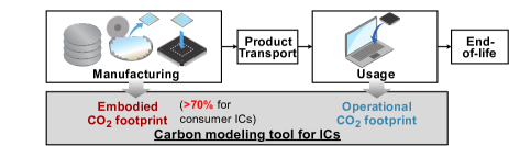
For decades, Moore’s Law has driven Integrated Circuits (ICs) to have greater computational power while being cheaper, smaller, and more energy-efficient. This has been the critical driving enabler for the development of new technologies, such as artificial intelligence (AI) [30]. However, the huge amount of carbon emissions associated with ICs, through their entire life cycle (see Fig. 1) from manufacturing, through deployment into usage, and finally into reuse, recycling, and disposal, have a non-negligible impact on environmental sustainability. As recently reported, the carbon footprint of Information and Communication Technology (ICT) accounts for about 2.1%3.9% of the world’s global greenhouse gas (GHG) emissions [15], which is proliferated to consume up to 8% in the near future [7].
To achieve environmental sustainability in ICs, it is necessary to address their carbon emissions across all life cycle phases, especially manufacturing and usage [18]. For today’s ICs, embodied carbon associated with IC manufacturing-related activities can often exceed operational carbon owing to energy consumption during usage [18]. This dominating emission source shift from operational to embodied carbon is the result of decades of operational energy efficiency optimization from ICs. In fact, embodied carbon can account for over 70% of the overall carbon footprint of consumer ICs [18, 12].
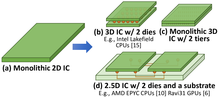
In parallel, as the pace of Moore’s Law in 2D monolithic ICs has slowed in recent years, research and development for ICs with advanced integration technologies, i.e., 3D and 2.5D ICs (see Fig. 2), has made significant progress. Various commercial products, prototypes, and studies have shown that 3D and 2.5D ICs can indeed offer substantial advantages over 2D ICs in terms of power, performance, area, and cost, e.g., see [14, 21, 22, 26, 20, 31, 4, 32]. However, there is a distinct lack of tools available to understand the carbon footprint of 3D and 2.5D ICs, especially embodied carbon emissions. Actually, such a carbon modeling tool is crucial for evaluating the sustainability of 3D and 2.5D ICs at the early design stage, given their increased complexity: On one hand, 3D/2.5D ICs require extra manufacturing steps, such as silicon thinning, via realization (e.g., Through-Silicon Via (TSV) and monolithic inter-tier via (MIV)), and bonding, increasing manufacturing carbon per wafer; On the other hand, the improved overall yield of dies [14, 4], the area savings [4], the heterogeneous technologies [4], and the reduced number of metal layers due to decreased interconnect distances [5] can potentially lower the carbon footprint per 3D/2.5D IC.
In this paper, we propose 3D-Carbon, a first-of-its-kind analytical carbon modeling tool that can capture the carbon footprint of commercial-grade 3D and 2.5D ICs. Based on hardware specifications, semiconductor fab characteristics, environmental factors, operational usage data surveyed from recent products and research papers, and third-party energy estimation plug-ins, 3D-Carbon estimates emissions from both IC manufacturing (i.e., embodied carbon) and usage (i.e., operational carbon). Using 3D-Carbon, we perform a series of case studies to optimize for total life cycle carbon and PPA (performance, power, and area) in the design strategies of 3D and 2.5D. We summarize our contributions as follows:
-
•
We develop 3D-Carbon, a first-of-its-kind analytical carbon modeling tool for 3D and 2.5D ICs. We believe that 3D-Carbon lays the initial foundation for future innovations in developing environmentally sustainable 3D and 2.5D ICs.
-
•
Using 3D-Carbon, we can predict the embodied carbon emissions associated with manufacturing without requiring precise knowledge of manufacturing parameters and estimate the operational carbon emissions during usage through surveyed parameters or third-party operational energy estimation plug-ins.
-
•
Through several case studies, we demonstrate the valuable insights and broad applicability of 3D-Carbon for three commercial-grade 2.5D integration technologies and three commercial-grade 3D integration technologies.
II Motivation And Background
II-A Lack of Tools Quantifying Emissions for 3D/2.5D ICs
Given the fact that ICs generate a huge amount of carbon emissions, academia and industry have developed a number of tools to quantify the life cycle carbon footprint of ICs [8, 11, 12, 18, 1]. These tools either rely on the database from industry [18, 1] or only provide coarse or first-order estimation [18, 11, 12, 8] for 3D/2.5D ICs. This section introduces and discusses the limitations of existing methods to motivate our proposed 3D-Carbon tool.
II-A1 Limitations of database-based carbon footprint modeling tools
Database-based tools take industry-provided data on materials [1] or manufacturing processes [18, 12] to estimate the carbon footprint of ICs. Although this approach allows for sustainability analysis when designing, its practicality and accuracy are constrained by the availability of up-to-date carbon emission data. For instance, ACT [18], which was developed as recently as 2022, does not support 3D/2.5D processors because of the absence of relevant databases.
II-A2 Limitations of coarse carbon footprint modeling tools
Due to the lack of data, a recent study [11] provides a first-order approach in which the embodied footprint per chip is roughly linearly proportional to the chip’s die size. Based on ACT [18], the follow-up study [12], denoted as ACT+ hereafter, approximates the embodied carbon footprint of the 2.5D IC from that of the corresponding 2D IC based on their cost comparison. For 3D ICs, ACT+ treats 3D stacked dies as 2D monolithic dies without considering the manufacturing and bonding overhead. While these area or cost-based proxies can be useful for giving general intuition, they do not offer detailed breakdowns needed for effective carbon-conscious design space exploration.
In contrast, 3D-Carbon is an analytical carbon modeling tool specifically designed for 3D/2.5D ICs. Compared to other approaches, this model provides a comprehensive estimation of the embodied carbon footprint by considering various factors such as technology node, wafer, metal layer count, yield, bonding, and packaging. 3D-Carbon can predict and estimate 3D/2.5D IC carbon emissions independently of industry reports and provide detailed breakdowns for further carbon-aware optimization. Additionally, 3D-Carbon utilizes parameters gathered from recent products and research papers, as well as third-party energy estimation plug-ins, such as the one in ACT+ [12], to provide up-to-date operational carbon estimation.
II-B Commercial-grade 3D/2.5D Integration Technologies
| 2.5 or 3D | Integration Technology | F2F or F2B | Stacking | # of max 3D dies/tiers | Representative Manufacturers | Representation Products/ Prototypes |
| 3D | Hybrid Bonding | F2F | D2W/W2W | 2 | TSMC’s SoIC-X [3] Intel’s Fevores Direct [24] | Arm Trisul test chip [25] |
| F2B | D2W/W2W | 2 | AMD Ryzen 7-5800X3D [31] | |||
| Micro- bumping | F2F | D2W/W2W | 2 | TSMC’s SoIC-P [3] Intel’s Fevores [24] | Intel Lakefield Core i5-L16G7 [16] | |
| F2B | D2W/W2W | 2 | HBM [21] | |||
| M3D | F2B | N/A | 2 | RISC-V Core◁ [22] | ||
| 2.5D | MCM | N/A | N/A | N/A | AMD’s Infinity Fabric [26] | AMD EPYC 7000 series [10] |
| InFO | N/A | N/A | N/A | TSMC’s InFO-2.5D CoWoS-L/R [3] | AMD Ravi 31 [6] (RDNA™ 3 [2]) | |
| Silicon Interposer | N/A | D2W | N/A | TSMC’s CoWoS-S [19] | Nvidia GPU P100 [28] |
-
•
◁: A M3D prototype uses GDS layout and sign-off quality simulation.
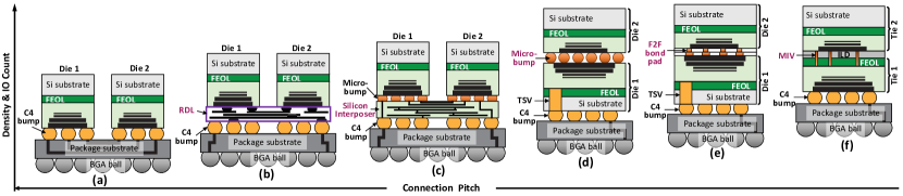
Various 3D and 2.5D integration approaches have been proposed. This section introduces three commercial-grade 3D integration technologies and three commercial-grade 2.5D integration technologies studied in this paper (see Table I). The concept of 3D-Carbon, however, can be extended to other 3D/2.5D integration technologies.
II-B1 3D integration
Micro-bumping 3D. In micro-bumping, multiple dies are stacked vertically with micron-level solder balls to establish the 3D connection. The pitch of the micro-bump is relatively larger than other technologies, with a 1050 diameter. Therefore, unlike other technologies, the IO driver for inter-die connections is necessary to transfer the signal properly through the micro-bump [22, 14]. A face-to-face (F2F) fashion is widely used in two-die micro-bumping integration (see Fig. 3 (d)), such as [16]. TSVs are required to connect signals and deliver power from the package to the 3D stack. By using face-to-back (F2B) fashion, 2 dies can be connected vertically [32] in which TSV provides connections between dies.
Hybrid Bonding 3D. Hybrid bonding uses bond pads to stack two 2D dies through the metal layers (see Fig. 3 (e)). The pitch of bond pad is much smaller than the micro-bumping, typically with 10 pitch.
Monolithic 3D (M3D). M3D integration (see Fig. 3 (f)) is a promising integration technology that utilizes sequential manufacturing techniques to provide fine-pitched MIVs (whose dimeters are typical 100nm) for inter-tier connections [22, 5]. M3D has three kinds of partitioning: block-level, gate-level, and transistor-level partitions. This paper focuses on block-level partition, where functional blocks (e.g., memory and logic macros) are partitioned into separate tiers, and gate-level partition, where gates are distributed across separate tiers, enabling the use of existing 2D process [5].
II-B2 2.5D integration
2.5D integration assembles multiple 2D dies, also known as chiplets, on a unifying substrate. Multi-chip module (MCM). MCM-based 2.5D IC directly deploys multiple pre-designed dies onto the organic package substrate (see Fig. 3 (a)). Integrated fan-out (InFO). Derived from fan-out wafer-level packaging, InFO utilizes a redistribution layer (RDL) (see Fig. 3 (b)) as the unifying substrate to provide smaller line space and thus better data rates than MCM. InFO can be divided into chip-first (TSMC’2 InFO-2.5D [3]) and chip-last (TSMC’s CoWoS-L/R [3]). Chip-last InFO allows for the integration of larger 2D dies with higher connection density and improved yield. However, this approach involves additional processes such as wafer bumping, chip-to-RDL substrate bonding, and underfilling, which result in increased carbon emissions per unit area [23]. Silicon interposer. Another widely used 2.5D integration technology is based on a substrate made of silicon (see Fig. 3 (c)). Silicon interposers can provide the finest line space, depending on the silicon technology utilized, but may significantly increase carbon cost. It is worth noting that silicon interposers can be either passive [28] or active [31].
II-C IC Carbon and Carbon Optimization Metrics
II-C1 IC total life cycle carbon
We follow the recent ACT [18] and ACT+ [12] to build the total life cycle carbon footprint model of an IC. The total carbon footprint () consist of both operational () and embodied () emissions. We introduce a relative ratio following the ACT+ approach [12], to facilitate the sweeping of the pareto-optimal curve of versus using : When using clean fab and with renewable energy for usage .
| (1) |
The operational carbon () due to the energy consumption during usage is the product of the energy () consumed by the IC during usage and the usage-phase carbon intensity ().
| (2) |
The embodied carbon footprint () is an amortized embodied carbon based on the application run-time (), and the overall execution time () of the IC.
| (3) |
For 2D ICs, the overall embodied carbon footprint () incurs the manufacturing emissions of semiconductor fabrication () and the packaging emissions ().
| (4) |
ACT assumes a constant packaging footprint for all ICs, which is not applicable to 3D/2.5D ICs due to the variability in package areas. 2D IC’s manufacturing carbon equation is as follows:
| (5) |
where is the carbon intensity of the fab’s electrical grid (location), is fab energy per unit 2D die area, is direct fab gas emissions per area, is carbon footprint from procuring raw materials for fab manufacturing per area, is 2D die area, and is the 2D die yield.
II-C2 Carbon optimization metrics
In [18, 12], various carbon-centric optimization metrics are presented to address the balance between carbon emissions and performance/energy consumption. These metrics encompass embodied carbon-centric measures like embodied carbon-delay product (CDP) and embodied carbon-energy product (CEP), along with the metric that encompasses total carbon emissions, termed as total carbon-delay product (tCDP).
III High-Level 3D-Carbon Tool
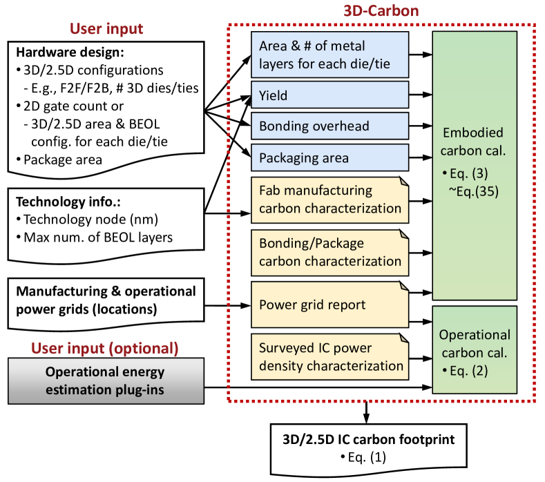
Fig. 4 illustrates the high-level carbon footprint modeling, encompassing both 3D/2.5D IC manufacturing (i.e., embodied carbon) and usage (i.e., operational carbon), that underscores 3D-Carbon. In order to estimate the embodied carbon footprint of 3D/2.5D ICs, 3D-Carbon leverages a hardware design description consisting of 3D/2.5D configurations and IC area-related details, a technology information description that includes the technology node and the maximum number of back-end-of-line (BEOL) layers, as well as the manufacturing grid (location) to find the corresponding carbon intensity (i.e., ). It should be noted that 3D-Carbon supports two approaches for IC area-related details: a comprehensive 3D/2.5D die area, back-end-of-line (BEOL) configuration description, and package area, as well as the utilization of a 2D IC gate count as an early design description for 3D/2.5D ICs. Based on the 2D IC gate count, 3D-Carbon predicts the 3D/2.5D area, the required number of BEOL layers, and the package area using surveyed area scaling and estimation methodologies [29].
In addition, for operational carbon footprint, 3D-Carbon can interface with operational energy estimation plug-ins, such as [17, 12], to estimate the energy consumption of applications executed on the 3D/2.5D ICs. Alternatively, 3D-Carbon can utilize surveyed IC power density characterization to predict energy consumption.
The 3D-Carbon model mainly focuses on logic technologies currently (i.e., logic and SRAM memory circuits). We hope 3D-Carbon encourages the industry to publish more detailed carbon characterization to extend 3D-Carbon to memories like HBM [21].
IV 3D-Carbon: Embodied Carbon Footprint
IV-A Embodied Carbon Footprint Model Parameters
3D-Carbon’s embodied carbon model integrates four types of parameters outlined in Table II. The hardware design related parameters are derived from the input file, while the foundry related parameters are relative to a given technology node from fab manufacturing carbon characterization [9]. Similarly, the bonding/packaging related parameters are acquired from bonding/packaging characterizations [13, 27]. To determine the global carbon efficiency for energy production, we refer to the power grid summary provided in [18]. We integrate the up-to-date yield parameters and models from [14], encompassing technologies, RDL process, and silicon interposer.
| Parameter | Description | Range |
| Hardware design related parameters | ||
| Integration | 3D/2.5D integration technology | Hybrid/Micro/M3D /MCM/InFO/Si_int |
| Facing | F2F or F2B for 3D | F2F or F2B |
| Stacking | Stacking approach for 3D | D2W or W2W |
| Num. of 3D/2.5D dies/ties | ||
| Area of die | User input (optional) | |
| Num. of BEOL layers of die | User input (optional) | |
| 2D gate count of die | User input (optional) | |
| Yield of the die in 3D/2.5D ICs | 01 | |
| Yield of the die alone | 01 | |
| Application run-time | Operational energy plug-ins | |
| Overall execution time | 110 years | |
| Foundary related parameters | ||
| Process | Process node | 3nm 28nm |
| IO driver area overhead ratio | 01 | |
| Pitch of TSVs | 420 | |
| GHG from fab | 0.10.5kg | |
| Manufacturing materials | 0.50 kg | |
| FEOL fab energy | 0.240.56 | |
| MOL fab energy | 0.080.23 | |
| BEOL metal layer fab energy | 0.61.81 | |
| Bonding related parameters | ||
| Yield of bonding between die and die in 3D ICs | 01 | |
| Yield of bonding between die and die alone | 01 | |
| Yield of bonding between die and substrate in 2.5D ICs | 01 | |
| Yield of bonding between die and substrate alone | 01 | |
| Yield of RDL substrate in InFO-based 2.5D ICs | 01 | |
| Yield of RDL substrate alone | 01 | |
| Yield of silicon interposer in silicon interposer 2.5D ICs | 01 | |
| Yield of silicon interposer alone | 01 | |
| Substrate area ratio | ||
| Bonding carbon per area | Bonding characterization | |
| RDL carbon per area | RDL characterization | |
| D2W and W2W bonding energy | 0.92.75 | |
| Packaging related parameters | ||
| Package area ratio | ||
| Packaging carbon per area | Package characterization | |
| Power grid related parameters | ||
| Fab intensity | 30700g /kWh | |
| Usage intensity | 30700g /kWh | |
IV-B Embodied Carbon Footprint Model
For 3D/2.5D ICs, the embodied carbon footprint is the same as Eq. (3). Unlike 2D ICs, 3D/2.5D ICs integrate several ( in our model) 2D dies and incur bonding carbon emissions. For silicon interposer based 2.5D ICs, an extra silicon interposer is also manufactured. We include die manufacturing emissions for all dies (), bonding emissions (), packaging carbon (), as well as a dedicated 2.5D substrate carbon () for the unifying substrate for InFO-based and silicon interposer-based 2.5D to formulate the overall embodied carbon footprint () as follows:
| (6) |
To calculate the embodied carbon emissions of each die (denoted as die ) in 3D/2.5D ICs, we begin by determining the carbon emissions per wafer () for this specific die. We then utilize the die-per-wafer count () and the yield of the die () in this 3D/2.5D ICs in the following equation:
| (7) |
In 3D-Carbon, the estimation of the packaging carbon footprint takes into account the packaging carbon emissions per area (), which is specific to the type of package technology used (e.g., PCBGA and MLCSP as mentioned in [27]), as well as the package area (). This allows for an accurate estimation of the carbon emissions associated with the packaging of the ICs.
| (8) |
Due to the variations in bonding carbon emissions between 3D and 2.5D ICs, 3D-Carbon develops precise carbon estimation approaches for 3D and 2.5D ICs. In addition, InFO-based and silicon interposer-based 2.5D ICs have specific carbon emissions for the RDL and silicon substrate; while in MCM-based 2.5D integration, the bonding and substate carbon emissions are combined into packaging footprints due to the use of an organic package substrate as a unifying substrate, serving both bonding and packaging purposes.
IV-B1 3D IC bonding footprint
3D ICs use wafer-to-wafer (W2W) or die-to-wafer (D2W) integration technologies for micro-bumping and hybrid bonding that stacks several separately pre-fabricated dies/wafers [13]. Therefore, similar to die carbon emissions, the bonding carbon emissions for 3D ICs are also derived from bonding carbon emissions per wafer () for this die . Note that in our notation, we refer to the die farthest away from the package substrate as die , while the die directly connected to the package substrate is denoted as die . The bonding carbon emission for the integration between die and die is denoted as , contributing to the overall bonding footprint as follows:
| (9) | ||||
IV-B2 2.5D IC bonding footprint
For InFO-based 2.5D ICs, the bonding carbon footprint is determined by multiplying the bonding carbon emissions per area () with the RDL area () and the yield of the bonding ().
| (10) |
In the case of silicon interposer-based 2.5D ICs, we assume D2W integration and micro-bumping technology. Given that manufacturing the wafer for silicon interposer consumes carbon emissions and the silicon interposer-per-wafer count is , 3D-Carbon formulate the bonding carbon footprint of silicon interposer-based 2.5D ICs as:
| (11) | ||||
IV-B3 2.5D IC substrate footprint
InFO-based 2.5D ICs utilize RDL as the substrate, we define the substrate carbon footprint based on RDL carbon emissions per area () and the yield of RDL process ()
| (12) |
The embodied carbon footprint () of the silicon interposer corresponds to the substrate footprint in silicon interposer-based 2.5D ICs. We employ a similar approach used for calculating the embodied carbon of silicon dies to estimate the substrate footprint.
| (13) |
IV-C Embodied Carbon Footprint Model Components
IV-C1 Area
As discussed in Sec. III, 3D-Carbon provides users with the option to use the 2D IC gate count as an early design description for determining 3D/2.5D IC area-related details. We present the methodologies employed by 3D-Carbon to predict the comprehensive area and back-end-of-line (BEOL) configurations based on the provided 2D IC gate count. Subsequently, we utilize the predicted areas and BEOL configurations to estimate the remaining parameters.
3D/2.5D gate die area. We first estimate the 2D IC area () given the technology node and gate count () as follows:
| (14) |
where is the feature size and is an empirical scaling term such that is the average area per gate. The surveyed values of for previous commercial products can be found in [29], where values range from 450 million for dense graphics processors, 700 million for consumer CPUs, and up to 850 million for certain system-on-chips.
From the given , users have the option to specify the die area ratio for each die. Alternatively, 3D-Carbon uses a default value for the gate area () for the dies/ties in 3D/2.5D ICs, which is calculated as follows:
| (15) |
To provide a more accurate estimation of die area, we account for additional overhead in 3D/2.5D ICs, i.e., the inclusion of potential TSVs and IO drivers in 3D ICs and IO drivers in 2.5D ICs.
3D die area. The estimation of the overall die area for the die of dies in 3D ICs is as follows:
| (16) |
where and is the potential TSVs area and IO driver area overhead, respectively.
The estimation of die area overhead in 3D ICs depends on the specific 3D integration technology and the choice between F2F and F2B. We categorize the estimation into five categories: F2F micro-bumping 3D, F2B micro-bumping 3D, F2F hybrid bonding 3D, F2B hybrid bonding 3D, and M3D.
F2F micro-bumping 3D. Referring to [14, 10], we consider an IO driver area overhead ratio () of the die gate area () to accommodate the additional area needed for IO drivers in both dies. TSVs are inserted in the bottom die (i.e., the die which is connected to the package substrate) to connect signals to the package. In F2F micro-bumping 3D integration, TSVs are inserted in the bottom die (i.e., die connected to the package substrate) for signal connection to the package. To accurately estimate the area overhead for TSVs, we require the user to provide the number of signals () to the package. If this information is not provided, a default value of 0 is assigned to , assuming no area overhead for TSVs. In summary, the die areas are ( is the dimension of TSVs):
| (17) | ||||
| (18) | ||||
| (19) |
F2B micro-bumping 3D. In contrast to the F2F 3D ICs, the use of TSVs enables connections between die and die in the vertical stack of the F2B 3D ICs. In addition, there is no need for TSVs in the bottom die (die ). We calculate the number of connection TSVs () following [29]
| (20) | |||
where and are the gate counts of two adjacent dies and other parameters are rent’s rule coefficients.
The dia areas other than the bottom die in F2B micro-bumping 3D are:
| (21) | ||||
| (22) |
The bottom die’s area (i.e., the die ) is:
| (23) |
F2F and F2B hybrid bonding 3D. The estimation of die areas in F2F and F2B hybrid bonding 3D ICs is similar to that of F2F and F2B micro-bumping 3D ICs, respectively, with the exception that there is no IO driver overhead. For the sake of simplicity, we do not delve into the detailed equations.
M3D. For the block-level and gate-level M3D, the die area is estimated to be approximately 50% of the corresponding 2D IC (i.e., in Eq. (15)) [5], unless otherwise specified.
BEOL configuration. The estimation of the number of BEOL layers () can be based on the following formulas which estimates the average wire length () of die [29]:
| (24) |
where . is the average fanout, is the wire pitch, is the average interconnect utilization rate, and other parameters are as Eq. (IV-C1). In cases where the estimated exceeds the maximum number of BEOL layers constraint specified in the technology file, 3D-Carbon adjusts the die area accordingly to ensure compliance with the constraint.
Bonding area. We specify the bonding area to be the same as the corresponding die area.
Package area. For vertically stacked 3D ICs, we employ an empirical equation that establishes a linear relationship between the maximum stacked die area and the package area () using an empirical scaling factor .
| (25) |
For 2.5D ICs, we adopt a similar method but use the total die area:
| (26) |
2.5D unifying substrate area. Similarly, empirical scaling factors, denoted as , are introduced to estimate the areas of the 2.5D RDL and silicon interposer unifying substrate.
| (27) |
IV-C2 Wafer carbon footprint
Extending Eq. 5, 3D-Carbon formulates the wafer carbon footprint () for die as follows:
| (28) |
The fab energy per unit area () is simply the sum of the individual energy cost of each layer:
| (29) | ||||
IV-C3 Bonding carbon footprint per wafer
The bounding energy per unit area is determined by the choice of D2W or W2W and the choice of micro-bumping or hybrid bonding. Therefore, the bonding carbon footprint per wafer is:
| (30) |
IV-C4 Die-per-wafer
IV-C5 Yield
We present the different components for the yield calculation first and then provide the yield calculation approaches for 3D/2.5D ICs.
2D die yield. We use the negative binomial yield model [4] which considers the defect density and the cluster of the manufacturing defects to calculate the 2D die yield () in the 3D/25D ICs.
3D stacked die and bonding yield. In D2W stacking, each die can be tested before bonding, while in W2W stacking, each die can usually be tested only after bonding. Therefore, the die yield () and bonding yield () are different for D2W and W2W approaches.
D2W. For D2W stacking, the resulting yields are as follows:
| (32) | ||||
W2W. For W2W stacking, the corresponding yields are:
| (33) | |||
2.5D die yield. The differences between chip-first and chip-last InFO-based 2.5D are viewed in 3D-Carbon.
Chip-first InFO. For chip-first InFO-based 2.5D ICs, the yields are:
| (34) | ||||
Chip-last 2.5D. Since silicon interposer adopts the chip-last approach as well, we summarize the yields for both chip-last InFO- and silicon interposer-based 2.5D as follows:
| (35) | ||||
V Model Comparison and Discussion
In this section, we provide a comparative analysis of the embodied carbon emissions and carbon optimization metrics obtained from our proposed 3D-Carbon and ACT+ [12], which, to our knowledge, is the only work available for studying carbon emissions in 3D/2.5D ICs. Compared with ACT+’s coarse modeling (see Sec. II-A), 3D-Carbon includes the influence of complex manufacturing, bonding, and packaging, and provides a detailed breakdown of the emissions.
V-A Comparison and Discussion of 3D IC Embodied Carbon
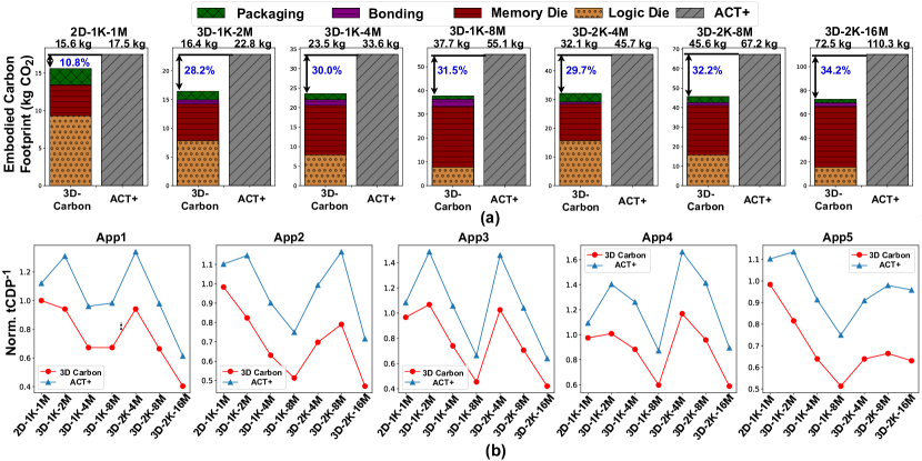
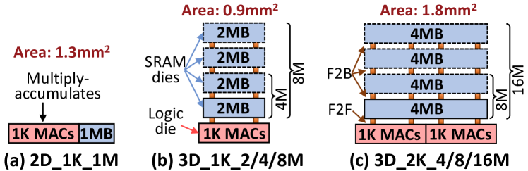
In [32], a series of 3D AR/VR accelerator prototypes is proposed to increase the on-chip SRAM memory capacity within the same chip area footprint, meeting the stringent form factor requirement. Fig. 7 shows the 2D baseline architecture alongside six 3D memory-stacked configurations. These configurations involve the vertical integration of one logic die with 1K or 2K MACs (multiple-accumulates) and 14 SRAM memory dies using hybrid bonding. The logic and SRAM dies employ 7nm technology. Different from a fixed standard BEOL configuration in ACT+, 3D-Carbon estimated the required number of BEOL layers using Eq. (24). Note that the bonding between the logic and SRAM dies follows the F2F approach, while multiple SRAM dies utilize the F2B approach for bonding. Additionally, we assume W2W stacking.
Fig. 6 (a) shows the total embodied carbon footprint using 3D-Carbon and ACT+ [12]. As ACT+, we use the globel grid for based on location. 3D-Carbon’s estimation demonstrates 10.8%34.2% less embodied emissions, despite accounting TSV and bonding overhead. This reduction is attributed to two factors that ACT+ excludes: (1) the use of fewer BEOL layers than ACT+ assumed due to small area (0.9 1.8 ) and decreased interconnect distances, leading to lower manufacturing carbon emissions, and (2) the compact form factor of the accelerator, reducing packaging carbon emissions. Fig. 6 (b) shows the normalized tCDP-1 metric. 3D-Carbon shows that even for a smaller SRAM capacity of 2M, 3D IC demonstrates a better trade-off than the 2D baseline for all considered five applications, motivating the shift to 3D ICs.
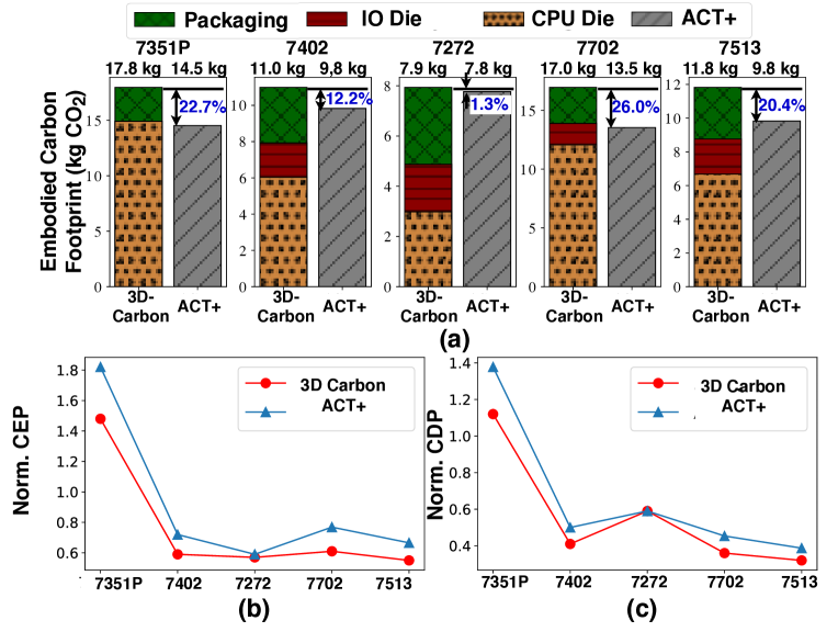
V-B Comparison and Discussion of 2.5D IC Embodied Carbon
Fig. 6 displays the carbon analysis outcomes for a series of AMD MCM 2.5D CPUs [10]. The CPU dies and IO dies are configured according to the specifications outlined in [10], utilizing different technology nodes: 14nm for CPU dies with IO driver circuits in 7351P and 7nm/14nm for CPU dies/IO dies in the remaining CPUs, respectively. Unlike ACT+, our 3D-Carbon model takes into account the manufacturing complexity: Firstly, we consider the BEOL configurations and set accordingly, recognizing that the CPU dies in 7351P have three more BEOL layers compared to the fixed configuration adopted in ACT+, while the CPU dies in other CPUs have two less BEOL layer compared to the fixed configuration assumed in ACT+; Secondly, we estimate packaging carbon emissions by considering the package area, which results in much higher (4288g) values compared to the fixed packaging carbon emissions (150g) in ACT+; Lastly, we enhance our model with more an up-to-date yield estimation.
Fig. 6 (a) illustrates the comparison of embodied carbon footprint estimated by two models. 3D-Carbon estimates embodied carbon emissions 1.3%26.0% higher than ACT+ due to its consideration of manufacturing complexity and yield, despite both models showing a similar trend. Using 3D-Carbon, we highlight the necessity of reducing packaging carbon emissions for CPUs with a smaller number of dies. In the case of 7272 with 2 CPU dies, packaging carbon emissions contribute to 32.7% of the total carbon footprint. Fig. 6 (b) and (c) demonstrate the CDP and CEP metrics, with 3D-Carbon identifying 7513 as the CEP-optimal configuration and ACT+ selecting 7272.
VI Carbon Efficient Design Space Exploration
VI-A Carbon Footprint Exploration
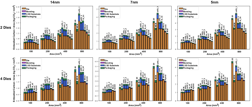
With 3D-Carbon for 2.5D and 3D ICs, the embodied carbon emissions at different design sizes and different process nodes can be compared to determine the switching points of the different 3D/2.5D integration technologies. This set of analyses encompasses both chip-first (InFO_1) and chip-last (InFO_2) approaches for InFO-based 2.5D designs, considering D2W stacking for all configurations. Notably, F2F bonding is employed for micro-bumping and hybrid bonding 3D in the case of 2 dies, while F2B bonding is utilized for the case of 4 dies. Since there is currently no 4-tier design available for M3D, we exclude M3D from the 4-die analysis.
Comparing 2D, 2.5D, and 3D ICs in Fig. 8, 3D ICs generally exhibit a reduced embodied carbon footprint compared due to their stacked dies with improved yield and constrained packaging overhead. The environmental sustainability advantages of 2.5D ICs are more pronounced for larger die areas (see Table III). Among the three types of 3D ICs, M3D and hybrid bonding 3D exhibit smaller embodied carbon emissions compared to micro-bumping 3D, primarily due to the absence of IO driver overhead. In terms of 2.5D ICs, chip-first InFO-based 2.5D ICs have a larger carbon footprint due to lower yield, while MCM-based 2.5D ICs are more carbon-efficient. However, the selection of the 2.5D IC type also depends on the required inter-die communication rate, with the other two 2.5D approaches supporting higher communication rates. In these scenarios, having a larger number of dies tends to result in lower embodied carbon emissions.
| Node | Num. of dies | Param. | MCM | InFO_2 | InFO_2 | Si_int | Micro | Hybrid | M3D |
| 14nm | 2 dies | 2D area | 210 | Inf | 981 | 831 | 60 | 45 | 0 |
| Gates (M) | 4734 | Inf | 22121 | 18756 | 1369 | 1173 | 0 | ||
| 4 dies | 2D area | 90 | 881 | 483 | 483 | 168 | 158 | N/A | |
| Gates (M) | 4664 | 45194 | 24791 | 24791 | 9066 | 8063 | N/A | ||
| 7nm | 2 dies | 2D area | 110 | 1329 | 657 | 659 | 89 | 83 | 0 |
| Gates (M) | 12491 | 29973 | 14830 | 14850 | 9921 | 9782 | 0 | ||
| 4 dies | 2D area | 60 | 1553 | 533 | 433 | 157 | 139 | N/A | |
| Gates (M) | 17442 | 169061 | 46054 | 13523 | 12319 | 9319 | N/A | ||
| 5nm | 2 dies | 2D area | 185 | Inf | 682 | 608 | 85 | 80 | 0 |
| Gates (M) | 9489 | Inf | 34992 | 31167 | 4389 | 4064 | 0 | ||
| 4 dies | 2D area | 85 | 583 | 384 | 359 | 283 | 253 | N/A | |
| Gates (M) | 9319 | 63469 | 41809 | 39102 | 23469 | 19865 | N/A |
VI-B Analysis of Carbon Efficiency for 3D ICs
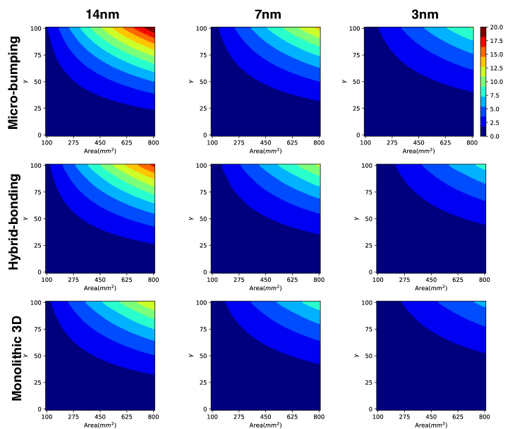
We sweep the relative ratio between operational and embodied carbon emissions to generate the trade-offs with the graph shown in Fig. 9. When using clean fab and with renewable energy for usage . Fig. 9 normalizes the resulting tCDP of 3D ICs to that of the 14nm 2D IC with 400 mm2 area and . A lower tCDP signifies a more favorable balance between overall carbon emissions and performance.
We show that the following trends hold for 3D ICs: Firstly, for small values of , indicating a focus on reducing embodied carbon emissions (or using clear fab), 3D ICs demonstrate better carbon efficiency due to their lower embodied carbon overhead and potential performance improvements; Secondly, as increases or chip area expands, micro-bumping 3D ICs tend to exhibit poorer tCDP first, highlighting the advantages of hybrid bonding and M3D in terms of carbon efficiency. However, it is important to consider other factors such as cost and signal integrity effects when evaluating these 3D approaches for real-world applications; Lastly, despite the manufacturing carbon overhead, advanced process nodes generally result in better carbon efficiency for 3D ICs.
VII Conclusion
To address the distinct lack of tools for understanding the carbon footprint of 3D and 2.5D ICs, coupled with the increasing prevalence of these advanced integration technologies, this work presents 3D-Carbon, a first-of-its-kind analytical carbon modeling tool that can capture the carbon footprint of commercial-grade 3D and 2.5D ICs at the early design stage. We believe that 3D-Carbon lays the initial foundation for future innovations in developing environmentally sustainable 3D and 2.5D ICs.
References
- [1] S. 2021, “Life Cycle Assessment Software.” https://sphera.com/product-sustainability-software/, 2021.
- [2] A. 2022, “AMD RDNA™ 3 Architecture with Chiplet Design,” https://www.amd.com/en/newsroom/press-releases/2022-11-3-amd-unveils-world-s-most-advanced-gaming-graphics-.html, 2022.
- [3] T. 2023, “TSMC 2023 North America Technology Symposium Overview,” https://semiwiki.com/semiconductor-manufacturers/tsmc/328139-tsmc-2023-north-america-technology-symposium-overview-part-3/, 2023.
- [4] A. Agnesina, M. Brunion, J. Kim, A. Garcia-Ortiz, D. Milojevic, F. Catthoor, M. Perumkunnil, and S. K. Lim, “Power, performance, area and cost analysis of memory-on-logic face-to-face bonded 3d processor designs,” in 2021 IEEE/ACM International Symposium on Low Power Electronics and Design (ISLPED). IEEE, 2021, pp. 1–6.
- [5] I. Akgun, D. Stow, and Y. Xie, “Network-on-chip design guidelines for monolithic 3-d integration,” IEEE Micro, vol. 39, no. 6, pp. 46–53, 2019.
- [6] AMD, “AMD Navi 31,” https://www.techpowerup.com/gpu-specs/amd-navi-31.g998, 2023.
- [7] A. S. Andrae and T. Edler, “On global electricity usage of communication technology: trends to 2030,” Challenges, vol. 6, no. 1, pp. 117–157, 2015.
- [8] R. U. Ayres, “Life cycle analysis: A critique,” Resources, conservation and recycling, vol. 14, no. 3-4, pp. 199–223, 1995.
- [9] M. G. Bardon, P. Wuytens, L.-Å. Ragnarsson, G. Mirabelli, D. Jang, G. Willems, A. Mallik, A. Spessot, J. Ryckaert, and B. Parvais, “DTCO including sustainability: Power-performance-area-cost-environmental score (PPACE) analysis for logic technologies,” in 2020 IEEE International Electron Devices Meeting (IEDM). IEEE, 2020, pp. 41–4.
- [10] C. Constantinescu, “AMD EPYC™ 7002 Series – A Processor with Improved Soft Error Resilience,” in 2021 51st Annual IEEE/IFIP International Conference on Dependable Systems and Networks - Supplemental Volume (DSN-S), 2021, pp. 33–36.
- [11] L. Eeckhout, “A first-order model to assess computer architecture sustainability,” IEEE Computer Architecture Letters, vol. 21, no. 2, pp. 137–140, 2022.
- [12] M. Elgamal, D. Carmean, E. Ansari, O. Zed, R. Peri, S. Manne, U. Gupta, G.-Y. Wei, D. Brooks, G. Hills et al., “Design space exploration and optimization for carbon-efficient extended reality systems,” arXiv preprint arXiv:2305.01831, 2023.
- [13] EVG, “EVG Bonding,” https://www.evgroup.com/products/bonding/.
- [14] Y. Feng and K. Ma, “Chiplet actuary: a quantitative cost model and multi-chiplet architecture exploration,” in Proceedings of the 59th ACM/IEEE Design Automation Conference, 2022, pp. 121–126.
- [15] C. Freitag, M. Berners-Lee, K. Widdicks, B. Knowles, G. S. Blair, and A. Friday, “The real climate and transformative impact of ICT: A critique of estimates, trends, and regulations,” Patterns, vol. 2, no. 9, p. 100340, 2021.
- [16] W. Gomes, S. Khushu, D. B. Ingerly, P. N. Stover, N. I. Chowdhury, F. O’Mahony, A. Balankutty, N. Dolev, M. G. Dixon, L. Jiang, S. Prekke, B. Patra, P. V. Rott, and R. Kumar, “8.1 Lakefield and Mobility Compute: A 3D Stacked 10nm and 22FFL Hybrid Processor System in 12×12mm2, 1mm Package-on-Package,” in 2020 IEEE International Solid- State Circuits Conference - (ISSCC), 2020, pp. 144–146.
- [17] A. Guler and N. K. Jha, “Mcpat-monolithic: An area/power/timing architecture modeling framework for 3-d hybrid monolithic multicore systems,” IEEE Transactions on Very Large Scale Integration (VLSI) Systems, vol. 28, no. 10, pp. 2146–2156, 2020.
- [18] U. Gupta, M. Elgamal, G. Hills, G.-Y. Wei, H.-H. S. Lee, D. Brooks, and C.-J. Wu, “ACT: Designing sustainable computer systems with an architectural carbon modeling tool,” in Proceedings of the 49th Annual International Symposium on Computer Architecture, 2022, pp. 784–799.
- [19] P. K. Huang, C. Y. Lu, W. H. Wei, C. Chiu, K. C. Ting, C. Hu, C. Tsai, S. Y. Hou, W. C. Chiou, C. T. Wang, and D. Yu, “Wafer Level System Integration of the Fifth Generation CoWoS®-S with High Performance Si Interposer at 2500 mm2,” in 2021 IEEE 71st Electronic Components and Technology Conference (ECTC), 2021, pp. 101–104.
- [20] D. B. Ingerly, S. Amin, L. Aryasomayajula, A. Balankutty, D. Borst, A. Chandra, K. Cheemalapati, C. S. Cook, R. Criss, K. Enamul, W. Gomes, D. Jones, K. C. Kolluru, A. Kandas, G.-S. Kim, H. Ma, D. Pantuso, C. Petersburg, M. Phen-givoni, A. M. Pillai, A. Sairam, P. Shekhar, P. Sinha, P. Stover, A. Telang, and Z. Zell, “Foveros: 3D Integration and the use of Face-to-Face Chip Stacking for Logic Devices,” in 2019 IEEE International Electron Devices Meeting (IEDM), 2019, pp. 19.6.1–19.6.4.
- [21] H. Jun, J. Cho, K. Lee, H.-Y. Son, K. Kim, H. Jin, and K. Kim, “HBM (High Bandwidth Memory) DRAM Technology and Architecture,” in 2017 IEEE International Memory Workshop (IMW), 2017, pp. 1–4.
- [22] J. Kim, L. Zhu, H. M. Torun, M. Swaminathan, and S. K. Lim, “Micro-bumping, hybrid bonding, or monolithic? A PPA study for heterogeneous 3D IC options,” in 2021 58th ACM/IEEE Design Automation Conference (DAC). IEEE, 2021, pp. 1189–1194.
- [23] J. H. Lau, “Recent advances and trends in advanced packaging,” IEEE Transactions on Components, Packaging and Manufacturing Technology, vol. 12, no. 2, pp. 228–252, 2022.
- [24] R. Mahajan and S. Sane, “Advanced packaging technologies for heterogeneous integration,” in IEEE Hot Chip Conference, 2021, pp. 22–24.
- [25] T. McLaurin, F. Frederick, H. Perry, S. Hung, and S. Sinha, “Applying ieee std 1838 to the 3dic design trishul–a case study,” in 2021 IEEE European Test Symposium (ETS). IEEE, 2021, pp. 1–4.
- [26] S. Naffziger, N. Beck, T. Burd, K. Lepak, G. H. Loh, M. Subramony, and S. White, “Pioneering Chiplet Technology and Design for the AMD EPYC™ and Ryzen™ Processor Families : Industrial Product,” in 2021 ACM/IEEE 48th Annual International Symposium on Computer Architecture (ISCA), 2021, pp. 57–70.
- [27] P. Nagapurkar and S. Das, “Economic and embodied energy analysis of integrated circuit manufacturing processes,” Sustainable Computing: Informatics and Systems, vol. 35, p. 100771, 2022.
- [28] NVIDIA, “NVIDIA Tesla P100,” https://www.nvidia.com/en-us/data-center/tesla-p100/, 2023.
- [29] D. Stow, I. Akgun, R. Barnes, P. Gu, and Y. Xie, “Cost and thermal analysis of high-performance 2.5 d and 3d integrated circuit design space,” in 2016 IEEE Computer Society Annual Symposium on VLSI (ISVLSI). IEEE, 2016, pp. 637–642.
- [30] N. C. Thompson, K. Greenewald, K. Lee, and G. F. Manso, “The computational limits of deep learning,” arXiv preprint arXiv:2007.05558, 2020.
- [31] J. Wuu, R. Agarwal, M. Ciraula, C. Dietz, B. Johnson, D. Johnson, R. Schreiber, R. Swaminathan, W. Walker, and S. Naffziger, “3D V-Cache: the Implementation of a Hybrid-Bonded 64MB Stacked Cache for a 7nm x86-64 CPU,” in 2022 IEEE International Solid- State Circuits Conference (ISSCC), vol. 65, 2022, pp. 428–429.
- [32] L. Yang, R. M. Radway, Y.-H. Chen, T. F. Wu, H. Liu, E. Ansari, V. Chandra, S. Mitra, and E. Beigné, “Three-Dimensional Stacked Neural Network Accelerator Architectures for AR/VR Applications,” IEEE Micro, vol. 42, no. 6, pp. 116–124, 2022.