Dynamic twisting and imaging of moiré crystals
††preprint: APS/123-QEDThe electronic band structure is an intrinsic property of solid-state materials that is intimately connected to the crystalline arrangement of atoms. Moiré crystals, which emerge in twisted stacks of atomic layers, feature a band structure that can be continuously tuned by changing the twist angle between adjacent layers Li et al. (2010); Bistritzer and MacDonald (2011); Yankowitz et al. (2012); Carr et al. (2017). This class of artificial materials blends the discrete nature of the moiré superlattice with intrinsic symmetries of the constituent materials, providing a versatile platform for investigation of correlated phenomena whose origins are rooted in the geometry of the superlattice, from insulating states at “magic angles” Kim et al. (2017); Iglovikov et al. (2014); Cao et al. (2018a, b) to flat bands in quasicrystals Moon et al. (2019). Here we present a route to mechanically tune the twist angle of individual atomic layers with a precision of a fraction of a degree inside a scanning probe microscope, which enables continuous control of the electronic band structure in situ. Using nanostructured rotor devices, we achieve the collective rotation of a single layer of atoms with minimal deformation of the crystalline lattice. In twisted bilayer graphene, we demonstrate nanoscale control of the moiré superlattice periodicity via external rotations, as revealed using piezoresponse force microscopy McGilly et al. (2020). We also extend this methodology to create twistable boron nitride devices, which could enable dynamic control of the domain structure of moiré ferroelectrics Zheng et al. (2020); Woods et al. (2021); Yasuda et al. (2021). This approach provides a route for real-time manipulation of moiré materials, allowing for systematic exploration of the phase diagrams at multiple twist angles in a single device.
In conventional solid-state materials, the band structure is a fixed property determined by the composition and arrangement of atoms in a crystalline lattice. Many recent breakthroughs have been enabled by synthesis of crystals with novel band structures, ranging from the development of flat band materials that host correlated phases to the discovery of quantum-relativistic crystals whose low energy electronic band structures give rise to charges that mimic relativistic particlesWehling et al. (2014); Derzhko et al. (2015). A contrasting “bottom-up” approach is the realization of artificial quantum matter using platforms such as ultracold atoms and trapped ions, which benefit from exquisite control and tunability Goldman et al. (2016); Spielman et al. (2010, 2007). However, the weakness of many-body interactions in these artificial systems has hampered investigation of certain classes of correlated states, while access to low temperature regimes has proven challenging. Two-dimensional moiré materials merge the best of both approaches by pairing strong correlations (and access to non-trivial band topology) with the tunability afforded by twisted heterostructures, for example enabling simulation of the Hubbard model in triangular superlattices Hubbard (1963); Li et al. (2010); Bistritzer and MacDonald (2011); Yankowitz et al. (2012); Carr et al. (2017); Tang et al. (2020); Mak and Shan (2022); Pan et al. (2020).
Twisted moiré superlattices – consisting of two atomic crystals rotated by an angle – exhibit behavior that departs dramatically from that of the constituent monolayers and form a highly tunable platform for exploration of emergent phenomena driven by interactions. Such artificially layered systems can be created in the lab by isolating single atomic layers from a bulk crystal and stacking them in a precise configuration using micromanipulators, a technique known as “van der Waals epitaxy” Novoselov et al. (2004); Geim and Grigorieva (2013); Dean et al. (2010). The moiré interference pattern features a modulation of the relative alignment between sublattice atoms, thus yielding spatial variations in the tunneling amplitude and interlayer potential difference across the superlattice. At small rotations that yield flat bands, electronic interactions dominate over the kinetic energy, giving rise to a rich phase diagram that can be tuned with twist angle Bistritzer and MacDonald (2011); Yankowitz et al. (2019); Kim et al. (2017); Wu et al. (2019). For example, twisted bilayer graphene exhibits a constellation of correlated states at a “magic angle” of , including superconductivity, Mott insulators, and a quantum anomalous Hall effect Bistritzer and MacDonald (2011); Cao et al. (2018a, b). In semiconductor Group IV transition metal dichalcogenides (TMDs), a richer picture emerges because broken inversion symmetry and spin-orbit coupling lift the spin degeneracy in the +/-K valence bands, which can lead to the formation of many-body topological phases in twisted heterostructures Wu et al. (2019); Pan et al. (2020); Zeng et al. (2023); Cai et al. (2023).
The periodic structure of the superlattice can also be leveraged for a broad range of practical applications, from the creation of photonic crystals for nano-light Sunku et al. (2018) to tunable angle-dependent platforms for electrochemistry Yu et al. (2022). However, existing methods for the construction of moiré heterostructures lock the atomic arrangement of the superlattice in place after device fabrication, so investigation of multiple twist angles requires measurements of ensembles of devices with different disorder profiles, strain, electrostatic environments. This motivates our development of a new technology to dynamically rotate individual layers of an active device structure, which should allow for continuous investigation of phase diagrams as a function of angle in a highly controlled setting.
In this work, we present a method for real-time rotation of individual atomic layers with a precision of a fraction of a degree, which should enable unprecedented control over the topology of the band structure and electronic interactions in moiré superlattices. We demonstrate manipulation of the superlattice periodicity with nanoscale resolution in response to this angular rotation, achieved through direct imaging of the moire superlattice using piezoresponse force microscopy (PFM) McGilly et al. (2020). Furthermore, the proposed nanomechanical approach offers a precise method of tuning the device to targeted angles that may host interesting phenomena, such as “magic angles” in twisted bilayer graphene or specific angles that host topological insulator states Bistritzer and MacDonald (2011); Pan et al. (2020); Cao et al. (2018b, a); Wu et al. (2019); Zeng et al. (2023); Cai et al. (2023).
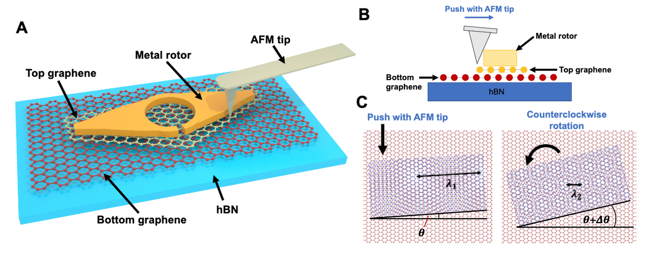
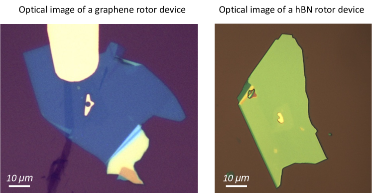
A schematic illustration of the rotor geometry and manipulation methodology is presented in Figure 1. We employ mechanical exfoliation and standard dry transfer methods to assemble twisted bilayer graphene and twisted double-layer hexagonal boron nitride (hBN) heterostructures, which are deposited onto a thicker hBN base layer Dean et al. (2010). As shown in Fig. 1 A, a nanostructured metal rotor is patterned on the top monolayer of the twisted heterostructure, allowing it to rotate freely with respect to the bottom flake. The rotor frame provides structural support that enables rigid rotation of the entire top atomic layer, minimizing the likelihood of stretching or tearing during the mechanical manipulation process. The rotors are patterned with electron beam (e-beam) lithography, followed by e-beam evaporation of 15 nm Cr / 100 nm Au (Fig. S1 in the Supplementary Information). The rotor is designed to cover most of the exposed area of the top monolayer, which allows the entire flake to move freely without being pinned onto the lower layer.
A Park NX20 scanning probe microscope with combined atomic force microscopy (AFM) and piezoresponse force microscopy (PFM) capabilities is used to both image and manipulate the twisted heterostructures in situ. As demonstrated in prior work, an AFM cantilever probe can be used to controllably apply lateral forces and move nanostructures (including multilayer hBN and graphite flakes) on a flat surface Koren et al. (2016); Chari et al. (2016); Ribeiro-Palau et al. (2018); Hu et al. (2022); Kapfer et al. (2022); Barabas et al. (2023); Yang et al. (2020); Inbar et al. (2023). Our in situ rotation process for twisted bilayer graphene is conceptually illustrated in Fig.1 B. When the moving AFM probe comes into contact with the metal rotor, it will exert a horizontal force on the structure. The adhesive force between the gold rotor frame and the top flake is considerably larger than the inter-layer friction and van der Waals forces between the graphene layers; therefore, the rotor-supported top flake will rigidly rotate on the surface of the bottom flake once the force exerted by the AFM probe exceeds the static friction limit between the two layers. Thus, the rotation process can be precisely controlled by programming the trace of the contact-mode AFM line scans. The rotation of the top layer with respect to the lower layer directly changes the moiré periodicity, as illustrated in Fig. 1 C.
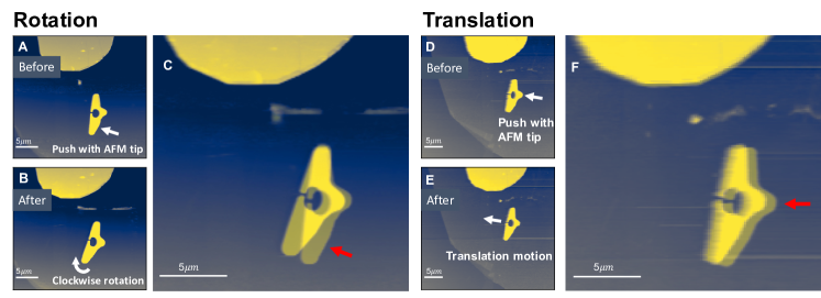
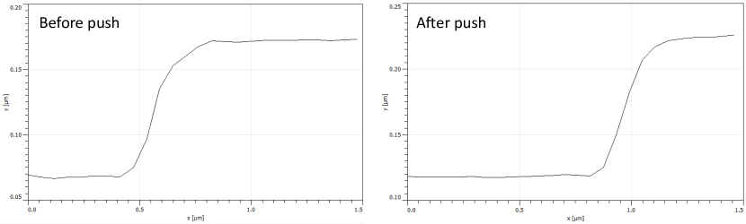
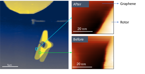
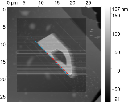
This in situ manipulation procedure allows for highly controlled translational and rotational inter-layer movement in twisted heterostructures, as shown in Fig. 2. The first step involves acquisition of a tapping-mode AFM image encompassing the entire metal frame and the surrounding area, which serves as a reference for later manipulation steps (Fig. 2 A, D). To obtain precise information on the initial orientation of the metal frame, high resolution AFM scans of the targeted pushing point on the lever arm are also obtained (Fig. S2 in the Supplementary Information). The manipulation process is performed with the AFM tip in contact mode, and the scanning direction of the tip should be oriented perpendicular to the lever arm of the rotor. The white arrow in Fig. 2A indicates the point of contact between the scanning tip and the rotor, and the resulting direction of the induced rotation is shown in Fig. 2B. When the AFM tip is scanned from the substrate towards the lever arm, the tip will push on the side wall of the rotor and a large longitudinal force exceeding is applied to the metal frame. (The forces required to achieve in situ twisting of double-layer graphene typically fall within the range of to .) Note that the contact-mode scan window should be defined to have a high aspect ratio or even be set to a single line scan, which pinpoints the specific location of the point of contact between the tip and rotor. The rotation angle can be tuned by changing the distance pushed by the AFM tip and the location of the point of contact on the rotor. Once the manipulation step is completed, another tapping-mode AFM image of the entire rotor frame and the surrounding area is obtained to quantify the induced rotation (Fig. 2B). To track the change in orientation of the rotor, Fig. 2 C plots the “before” and “after” images superimposed on top of each other. By comparing the two images, it is possible to resolve the twisting of the heterostructure (see Fig. S3 in the Supplementary Information). To more accurately identify the twist angle of the bilayer before and after the manipulation, PFM can be used to image the moiré pattern and extract its periodicity.
Fig. 2 D-F shows the second type of manipulation: lateral translation of the rotor. While tip-controlled manipulation can be used to induce both rotation and translation, their relative proportions can be controlled by adjusting the position of the push point. Nearly pure translation could be achieved by aligning the tip contact point with the center of mass of the metal rotor structure. The sliding resistance between the two graphene sheets arises mainly from interlayer friction and resistive forces caused by uneven topography and organic residues from nanofabrication. We find that contact-mode cleaning, a standard technique for improving the surface cleanliness of van der Waals heterostructuresGoossens et al. (2012); Lindvall et al. (2012), effectively reduces the sliding resistance between two layers by removing organic residues from the e-beam lithography process. Additionally, heating the sample stage decreases the interlayer friction, which facilitates the nanomechanical manipulation process.
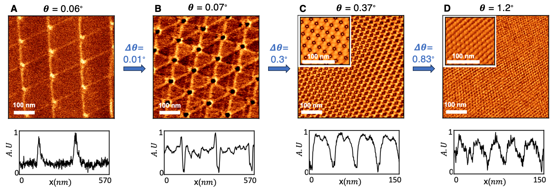
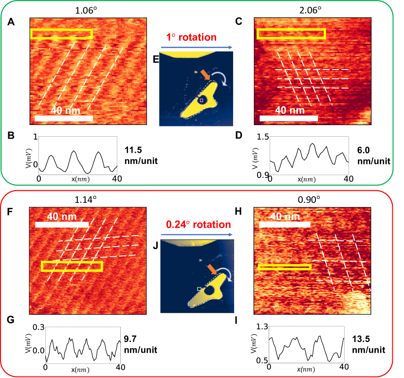
The main goal of this manipulation technique is to exert precise, controllable changes to the structure and unit cell size of a moiré crystal. In Fig. 3, we demonstrate dynamic rotation of a single monolayer within a twisted bilayer graphene heterostructure and observe a series of controlled changes in the superlattice period. During the rotation process, the device was tuned to four distinct twist angles: 0.06°, 0.07°, 0.37°, and 1.20°. The sequence of PFM images in Fig.3A-D show the evolution of the moiré pattern with twist angle; all scans were captured from the same location on the heterostructure. These images reveal nearly isotropic changes in the period of the superlattice for each successive twist angle change . The twist angle for each configuration can be extracted experimentally from the measured superlattice period, as discussed in the Supplementary Information. From the PFM data, we observe no obvious stretching or deformation introduced to the superlattice during the rotation process. This is one difference between the proposed approach and other methods for mechanical manipulation of van der Waals heterostructures, which can simultaneously introduce strain in the process. To show reproducibility, we also demonstrate the twisting-induced manipulation of the moiré superlattice in a separate twisted bilayer graphene device, which exhibits similar behavior (see Fig.S6 in the Supplementary Information).
To achieve the sequence of rotations featured in Fig.3A-D, the sample stage was heated up to to lower the interlayer friction between the graphene flakes, and the longitudinal forces used in the AFM manipulation process ranged from to . The smallest twist angle change that we could demonstrate experimentally is roughly , as illustrated in Fig. 3A-B, which was achieved by inducing a displacement of the rotor arm. The differences between the expected rotation angle (, estimated based on the lateral displacement of the lever arm) and the actual twist angle change (, extracted experimentally from the measured superlattice period) can be attributed to the natural scale errors in the AFM scanning program and the lateral deflection of the tip during the pushing process, which adds a small offset to the tip travel distance (see Supplementary Information for details). AFM images of the rotor device used for these measurements are provided in Supplementary Figs. S4-S5.
In order to demonstrate the broader applicability of this method for other classes of 2D materials, we extend this technique to twisted double-layer hBN, which for example could enable in situ tuning of the ferroelectric domain structure by changing the twist angle Zheng et al. (2020); Woods et al. (2021); Yasuda et al. (2021).
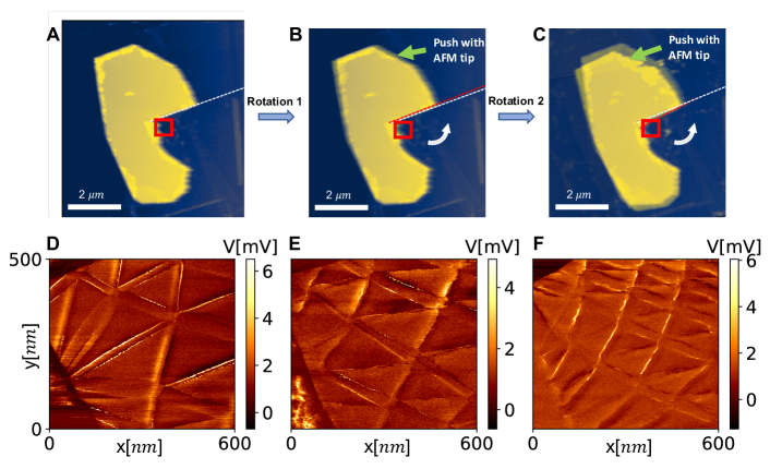
The fabrication procedure and heterostructure geometry are conceptually similar that illustrated schematically in Fig. 1A (see Fig.4 and Fig. S1 in the Supplementary Information).
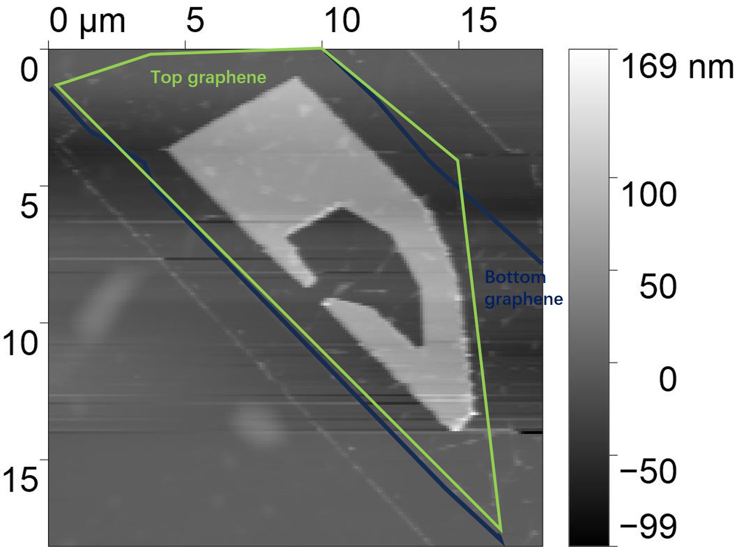
Fig. 4A-C show tapping-mode AFM images of the rotor configurations prior to manipulation, after the first rotation, and after the second rotation, respectively.
By manipulating the rotor, we are able to induce corresponding changes in the moiré domain structure, as revealed in the PFM images displayed in Fig. 4 D-F.
The longitudinal forces required to manipulate hBN rotors, which fall in the range of to , are typically smaller than those required to rotate twisted bilayer graphene.
Conclusion and Outlook. In contrast to many existing state-of-the-art twisted bilayer heterostructures, in which the atoms are locked into a specific configuration after fabrication, the devices presented here offer a new route to dynamically tune and image moiré superlattices. This is achieved via controlled rotation of a single atomic layer with respect to another, which can be performed in situ within a microscope. The high level of angular control provides access to multiple twist angles and superlattice configurations, which enables systematic investigation of a wide variety of phenomena within a single device. This method can also be extended to monolayer van der Waals materials beyond graphene, opening the door to dynamic control over the ferroelectric domain structure in angle-aligned hBN and TMDs Wang et al. (2022), or manipulation of the periodicity of topological spin textures in moiré magnetsXie et al. (2023).
The twisted heterostructure remains exposed throughout the entire rotation process to allow for easy interrogation with optical or scanning probes, which could be useful for a broad range of experiments across many scientific disciplines. The in situ twisting technique presented here does not require any specialized scanning probe microscopy instrumentation to perform; it can be implemented using a commercial AFM and nanofabrication equipment available in a standard cleanroom. We hope that this accessibility will allow for broad adoption of this methodology across the community.
Acknowledgements
We gratefully acknowledge funding support from the UC Office of the President, specifically the UC Laboratory Fees Research Program (award LFR-20-653926) and the AFOSR Young Investigator Program (award FA9550-20-1-0035). This work was performed, in part, at the San Diego Nanotechnology Infrastructure (SDNI) of UCSD, a member of the National Nanotechnology Coordinated Infrastructure, which is supported by the National Science Foundation (Grant ECCS-2025752).
References
- Li et al. (2010) Guohong Li, A Luican, JMB Lopes dos Santos, AH Castro Neto, A Reina, J Kong, and EY Andrei, “Observation of van hove singularities in twisted graphene layers,” Nature physics 6, 109–113 (2010).
- Bistritzer and MacDonald (2011) Rafi Bistritzer and Allan H MacDonald, “Moiré bands in twisted double-layer graphene,” Proceedings of the National Academy of Sciences 108, 12233–12237 (2011).
- Yankowitz et al. (2012) Matthew Yankowitz, Jiamin Xue, Daniel Cormode, Javier D Sanchez-Yamagishi, K Watanabe, T Taniguchi, Pablo Jarillo-Herrero, Philippe Jacquod, and Brian J LeRoy, “Emergence of superlattice dirac points in graphene on hexagonal boron nitride,” Nature physics 8, 382–386 (2012).
- Carr et al. (2017) Stephen Carr, Daniel Massatt, Shiang Fang, Paul Cazeaux, Mitchell Luskin, and Efthimios Kaxiras, “Twistronics: Manipulating the electronic properties of two-dimensional layered structures through their twist angle,” Physical Review B 95, 075420 (2017).
- Kim et al. (2017) Kyounghwan Kim, Ashley DaSilva, Shengqiang Huang, Babak Fallahazad, Stefano Larentis, Takashi Taniguchi, Kenji Watanabe, Brian J LeRoy, Allan H MacDonald, and Emanuel Tutuc, “Tunable moiré bands and strong correlations in small-twist-angle bilayer graphene,” Proceedings of the National Academy of Sciences 114, 3364–3369 (2017).
- Iglovikov et al. (2014) VI Iglovikov, F Hébert, B Grémaud, GG Batrouni, and RT Scalettar, “Superconducting transitions in flat-band systems,” Physical Review B 90, 094506 (2014).
- Cao et al. (2018a) Yuan Cao, Valla Fatemi, Ahmet Demir, Shiang Fang, Spencer L Tomarken, Jason Y Luo, Javier D Sanchez-Yamagishi, Kenji Watanabe, Takashi Taniguchi, Efthimios Kaxiras, et al., “Correlated insulator behaviour at half-filling in magic-angle graphene superlattices,” Nature 556, 80–84 (2018a).
- Cao et al. (2018b) Yuan Cao, Valla Fatemi, Shiang Fang, Kenji Watanabe, Takashi Taniguchi, Efthimios Kaxiras, and Pablo Jarillo-Herrero, “Unconventional superconductivity in magic-angle graphene superlattices,” Nature 556, 43–50 (2018b).
- Moon et al. (2019) Pilkyung Moon, Mikito Koshino, and Young-Woo Son, “Quasicrystalline electronic states in 30°rotated twisted bilayer graphene,” Physical Review B 99, 165430 (2019).
- McGilly et al. (2020) Leo J McGilly, Alexander Kerelsky, Nathan R Finney, Konstantin Shapovalov, En-Min Shih, Augusto Ghiotto, Yihang Zeng, Samuel L Moore, Wenjing Wu, Yusong Bai, et al., “Visualization of moiré superlattices,” Nature Nanotechnology 15, 580–584 (2020).
- Zheng et al. (2020) Zhiren Zheng, Qiong Ma, Zhen Bi, Sergio de La Barrera, Ming-Hao Liu, Nannan Mao, Yang Zhang, Natasha Kiper, Kenji Watanabe, Takashi Taniguchi, et al., “Unconventional ferroelectricity in moiré heterostructures,” Nature 588, 71–76 (2020).
- Woods et al. (2021) CR Woods, P Ares, H Nevison-Andrews, MJ Holwill, R Fabregas, Francisco Guinea, AK Geim, KS Novoselov, NR Walet, and L Fumagalli, “Charge-polarized interfacial superlattices in marginally twisted hexagonal boron nitride,” Nature communications 12, 347 (2021).
- Yasuda et al. (2021) Kenji Yasuda, Xirui Wang, Kenji Watanabe, Takashi Taniguchi, and Pablo Jarillo-Herrero, “Stacking-engineered ferroelectricity in bilayer boron nitride,” Science 372, 1458–1462 (2021).
- Wehling et al. (2014) Tim O Wehling, Annica M Black-Schaffer, and Alexander V Balatsky, “Dirac materials,” Advances in Physics 63, 1–76 (2014).
- Derzhko et al. (2015) Oleg Derzhko, Johannes Richter, and Mykola Maksymenko, “Strongly correlated flat-band systems: The route from heisenberg spins to hubbard electrons,” International Journal of Modern Physics B 29, 1530007 (2015).
- Goldman et al. (2016) Nathan Goldman, Jan C Budich, and Peter Zoller, “Topological quantum matter with ultracold gases in optical lattices,” Nature Physics 12, 639–645 (2016).
- Spielman et al. (2010) Ian B Spielman, Nathan Goldman, Indubala I Satija, Predrag Nikolic, Alejandro Bermudez, Miguel A Martin-Delgado, and Maciej Lewenstein, “Engineering time-reversal invariant topological insulators with ultra-cold atoms,” (2010).
- Spielman et al. (2007) Ian B Spielman, William D Phillips, and James V Porto, “Mott-insulator transition in a two-dimensional atomic bose gas,” Physical Review Letters 98, 080404 (2007).
- Hubbard (1963) Hubbard, “Electron correlations in narrow energy bands,” Proceedings of the Royal Society of London. Series A. Mathematical and Physical Sciences 281, 401–419 (1963).
- Tang et al. (2020) Yanhao Tang, Lizhong Li, Tingxin Li, Yang Xu, Song Liu, Katayun Barmak, Kenji Watanabe, Takashi Taniguchi, Allan H MacDonald, Jie Shan, et al., “Simulation of hubbard model physics in wse2/ws2 moiré superlattices,” Nature 579, 353–358 (2020).
- Mak and Shan (2022) Kin Fai Mak and Jie Shan, “Semiconductor moiré materials,” Nature Nanotechnology 17, 686–695 (2022).
- Pan et al. (2020) Haining Pan, Fengcheng Wu, and Sankar Das Sarma, “Quantum phase diagram of a moiré-hubbard model,” Physical Review B 102, 201104 (2020).
- Novoselov et al. (2004) Kostya S Novoselov, Andre K Geim, Sergei V Morozov, De-eng Jiang, Yanshui Zhang, Sergey V Dubonos, Irina V Grigorieva, and Alexandr A Firsov, “Electric field effect in atomically thin carbon films,” science 306, 666–669 (2004).
- Geim and Grigorieva (2013) Andre K Geim and Irina V Grigorieva, “Van der waals heterostructures,” Nature 499, 419–425 (2013).
- Dean et al. (2010) Cory R Dean, Andrea F Young, Inanc Meric, Chris Lee, Lei Wang, Sebastian Sorgenfrei, Kenji Watanabe, Takashi Taniguchi, Phillip Kim, Kenneth L Shepard, et al., “Boron nitride substrates for high-quality graphene electronics,” Nature nanotechnology 5, 722–726 (2010).
- Yankowitz et al. (2019) Matthew Yankowitz, Shaowen Chen, Hryhoriy Polshyn, Yuxuan Zhang, K Watanabe, T Taniguchi, David Graf, Andrea F Young, and Cory R Dean, “Tuning superconductivity in twisted bilayer graphene,” Science 363, 1059–1064 (2019).
- Wu et al. (2019) Fengcheng Wu, Timothy Lovorn, Emanuel Tutuc, Ivar Martin, and AH MacDonald, “Topological insulators in twisted transition metal dichalcogenide homobilayers,” Physical review letters 122, 086402 (2019).
- Zeng et al. (2023) Yihang Zeng, Zhengchao Xia, Kaifei Kang, Jiacheng Zhu, Patrick Knüppel, Chirag Vaswani, Kenji Watanabe, Takashi Taniguchi, Kin Fai Mak, and Jie Shan, “Integer and fractional chern insulators in twisted bilayer mote2,” arXiv preprint arXiv:2305.00973 (2023).
- Cai et al. (2023) Jiaqi Cai, Eric Anderson, Chong Wang, Xiaowei Zhang, Xiaoyu Liu, William Holtzmann, Yinong Zhang, Fengren Fan, Takashi Taniguchi, Kenji Watanabe, et al., “Signatures of fractional quantum anomalous hall states in twisted mote2 bilayer,” arXiv preprint arXiv:2304.08470 (2023).
- Sunku et al. (2018) SS Sunku, GuangXin Ni, Bor-Yuan Jiang, Hyobin Yoo, Aaron Sternbach, AS McLeod, T Stauber, Lin Xiong, Takashi Taniguchi, Kenji Watanabe, et al., “Photonic crystals for nano-light in moiré graphene superlattices,” Science 362, 1153–1156 (2018).
- Yu et al. (2022) Yun Yu, Kaidi Zhang, Holden Parks, Mohammad Babar, Stephen Carr, Isaac M Craig, Madeline Van Winkle, Artur Lyssenko, Takashi Taniguchi, Kenji Watanabe, et al., “Tunable angle-dependent electrochemistry at twisted bilayer graphene with moiré flat bands,” Nature Chemistry 14, 267–273 (2022).
- Koren et al. (2016) Elad Koren, Itai Leven, Emanuel Lörtscher, Armin Knoll, Oded Hod, and Urs Duerig, “Coherent commensurate electronic states at the interface between misoriented graphene layers,” Nature nanotechnology 11, 752–757 (2016).
- Chari et al. (2016) Tarun Chari, Rebeca Ribeiro-Palau, Cory R Dean, and Kenneth Shepard, “Resistivity of rotated graphite–graphene contacts,” Nano letters 16, 4477–4482 (2016).
- Ribeiro-Palau et al. (2018) Rebeca Ribeiro-Palau, Changjian Zhang, Kenji Watanabe, Takashi Taniguchi, James Hone, and Cory R Dean, “Twistable electronics with dynamically rotatable heterostructures,” Science 361, 690–693 (2018).
- Hu et al. (2022) Cheng Hu, Tongyao Wu, Xinyue Huang, Yulong Dong, Jiajun Chen, Zhichun Zhang, Bosai Lyu, Saiqun Ma, Kenji Watanabe, Takashi Taniguchi, et al., “In-situ twistable bilayer graphene,” Scientific Reports 12, 204 (2022).
- Kapfer et al. (2022) Mäelle Kapfer, Bjarke S Jessen, Megan E Eisele, Matthew Fu, Dorte R Danielsen, Thomas P Darlington, Samuel L Moore, Nathan R Finney, Ariane Marchese, Valerie Hsieh, et al., “Programming moir’e patterns in 2d materials by bending,” arXiv preprint arXiv:2209.10696 (2022).
- Barabas et al. (2023) Andrew Z Barabas, Ian Sequeira, Yuhui Yang, Aaron H Barajas-Aguilar, Takashi Taniguchi, Kenji Watanabe, and Javier D Sanchez-Yamagishi, “Mechanically reconfigurable van der waals devices via low-friction gold sliding,” Science Advances 9, eadf9558 (2023).
- Yang et al. (2020) Yaping Yang, Jidong Li, Jun Yin, Shuigang Xu, Ciaran Mullan, Takashi Taniguchi, Kenji Watanabe, Andre K. Geim, Konstantin S. Novoselov, and Artem Mishchenko, “In situ manipulation of van der waals heterostructures for twistronics,” Science Advances 6, eabd3655 (2020).
- Inbar et al. (2023) A. Inbar, J. Birkbeck, J. Xiao, T. Taniguchi, K. Watanabe, B. Yan, Y. Oreg, Ady Stern, E. Berg, and S. Ilani, “The quantum twisting microscope,” Nature 614, 682–687 (2023).
- Goossens et al. (2012) AM Goossens, VE Calado, A Barreiro, K Watanabe, T Taniguchi, and LMK Vandersypen, “Mechanical cleaning of graphene,” Applied Physics Letters 100 (2012).
- Lindvall et al. (2012) Niclas Lindvall, Alexey Kalabukhov, and August Yurgens, “Cleaning graphene using atomic force microscope,” Journal of Applied Physics 111 (2012).
- Wang et al. (2022) Xirui Wang, Kenji Yasuda, Yang Zhang, Song Liu, Kenji Watanabe, Takashi Taniguchi, James Hone, Liang Fu, and Pablo Jarillo-Herrero, “Interfacial ferroelectricity in rhombohedral-stacked bilayer transition metal dichalcogenides,” Nature nanotechnology 17, 367–371 (2022).
- Xie et al. (2023) Hongchao Xie, Xiangpeng Luo, Zhipeng Ye, Zeliang Sun, Gaihua Ye, Suk Hyun Sung, Haiwen Ge, Shaohua Yan, Yang Fu, Shangjie Tian, et al., “Evidence of non-collinear spin texture in magnetic moiré superlattices,” Nature Physics , 1–6 (2023).
Supplementary Information
The estimated rotation angle () extracted from the tapping-mode AFM images is calculated based on the push distance of the rotor and rotation radius. The pushing distance can be extracted from the 1D line scan curve before and after the push (Fig. S2), while the rotation radius is determined from superimposed tapping-mode AFM images (Fig. 2; Fig. S3). The push distance can be finely controlled by pausing the tip in the middle of the contact mode line scan. The rotation radius is determined by drawing extension lines along one straight edge of the rotor before and after the rotation; the cross point can be considered as the rotation center.
The actual twist angles extracted from the measured moiré patterns are calculated using the following equation:
where is the moiré periodicity, is the lattice constant, and is the twist angle. For a graphene lattice, . The moiré periodicity can be determined experimentally from the piezoresponse force microscopy images (Fig. 3; Fig. S6).