Spin-splitting in electric-potential-difference antiferromagnetism
Abstract
The antiferromagnetic (AFM) materials are robust to external magnetic perturbation due to missing any net magnetic moment. In general, the spin splitting in the band structures disappears in these antiferromagnets. However, the altermagnetism can achieve spin-split bands in collinear symmetry-compensated antiferromagnet with special magnetic space group. Here, we propose a new mechanism that can achieve spin splitting in two-dimensional (2D) Janus A-type AFM materials. Since the built-in electric field caused by Janus structure creates a layer-dependent electrostatic potential, the electronic bands in different layers will stagger, producing the spin splitting, which can be called electric-potential-difference antiferromagnetism (EPD-AFM). We demonstrate that Janus monolayer is a possible candidate to achieve the EPD-AFM by the first-principles calculations. It is proposed that the spin splitting can be tuned in EPD-AFM by piezoelectric effect. Our works provide a new design principle for generating spin polarization in 2D AFM materials.
I Introduction
The spin splitting in the band structures can be produced by utilizing the effect of spin-orbit coupling (SOC)gs1 . A general form of the SOC Hamiltonian in solid-state materials with a lack of inversion symmetry can be expressed asgs2 ; gs3 :
| (1) |
Where the is known as a spin-orbit field (SOF) as an effective magnetic field, is the strength of the SOC, is the local electric field induced by the crystal inversion asymmetry, is is the wave vector, and =(, , ) are the Pauli matrices.
If a two-dimensional (2D) material possesses out-of-plane built-in electric field, Equation 1 will become:
| (2) |
This is known as Rashba SOC Hamiltoniangs4 , and is the so-called Rashba parameter. Here, the spin only has the in-plane components and , which depend on the momentum of electrons. The impurities and defects can change the momentum of electrons, which can randomize the spin due to the -dependent SOF, and then induce spin decoherence through the Dyakonov-Perel (DP) mechanismgs5 .
If a 2D material possesses in-plane built-in electric field, for example along direction, Equation 1 will be reduced into:
| (3) |
Here, the spin only has the out-of-plane component . The SOF orientation of Equation 3 is unidirectional, which will lead to a spatially periodic mode of the spin polarization, known as the persistent spin helix (PSH)p7 ; p8 . The PSH can suppress spin dephasing due to SU(2) spin rotation symmetry, producing an extremely long spin lifetimep7 ; p9 .
The spin splitting can also be observed in ferromagnetic (FM) materials. Superior to FM materials, the antiferromagnetic (AFM) materials are robust to external magnetic perturbation due to missing any net magnetic moment, which allows high-speed device operationk1 ; k2 . In general, the spin splitting in the band structures is lacking in these antiferromagnets. However, the spin splitting has been realized in collinear symmetry-compensated antiferromagnet, and the SOC is not needed, which is called altermagnetismk4 ; k5 ; k6 . Several 2D materials have been predicted to be altermagnetic materials, such as k11 ; k12 , k12-1 and k13 .
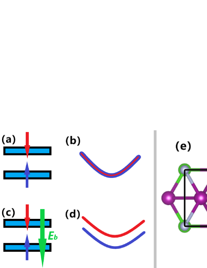
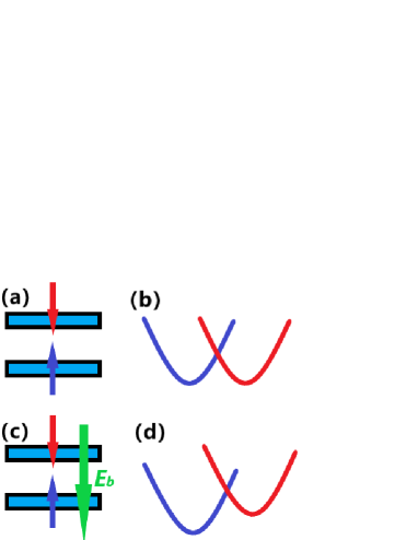
Here, we propose a new mechanism to achieve spin splitting in AFM materials. For a 2D material, the magnetic atoms have opposite layer spin polarization, namely A-type AFM ordering. If the out-of-plane built-in electric field is lacking, the degeneration of electron spin in the band structures is observed (Figure 1 (a) and (b)). For a 2D Janus material, the magnetic configuration is still A-type AFM ordering, but it has an out-of-plane built-in electric field , which will destroy the degeneration of electron spin in the band structures (Figure 1 (c) and (d)). This is because the built-in electric field creates a layer-dependent electrostatic potential, and the electronic bands in different layers will stagger, which gives rise to the spin splitting. The spin splitting in 2D Janus A-type AFM materials can be called electric-potential-difference antiferromagnetism (EPD-AFM).
Recently, the electric-field control of spin polarization in 2D A-type AFM semiconductor has been reported, and the 100% spin polarization via electric field can be achievedk14 . Based on , Janus monolayer is constructed by replacing one of two Cl layers with F atoms, which is proved to be a possible candidate to achieve the EPD-AFM by the first-principles calculations. Calculated results show that EPD-AFM in is robust against the electronic correlation. The piezoelectric properties of are also investigated, and the out-of-plane piezoelectric response may be used to tune the spin splitting. These findings enrich the types of spin splitting, which is useful for spintronic device applications.
II Computational detail
Within density functional theory (DFT)1 , the spin-polarized first-principles calculations are carried out within the projector augmented-wave (PAW) method by using the standard VASP codepv1 ; pv2 ; pv3 . We use the generalized gradient approximation of Perdew-Burke-Ernzerhof (PBE-GGA)pbe as the exchange-correlation functional. To account for electron correlation of Mn-3 orbitals, we use a Hubbard correction =4.00 eVu1 ; u2 ; u3 within the rotationally invariant approach proposed by Dudarev et al. The kinetic energy cutoff of 500 eV, total energy convergence criterion of eV, and force convergence criterion of 0.0001 are set to obtain the accurate results. A vacuum of more than 16 is used to avoid out-of-plane interaction.
The elastic stiffness tensor and piezoelectric stress tensor are calculated by using strain-stress relationship (SSR) method and density functional perturbation theory (DFPT) methodpv6 , respectively. The / has been renormalized by =/=, where the is the length of unit cell along direction. We use a 21211 k-point meshes to sample the Brillouin zone (BZ) for calculating electronic structures and elastic properties, and a 10211 k-point meshes for piezoelectric calculations. The interatomic force constants (IFCs) are calculated by using a 551 supercell within finite displacement method, and the phonon dispersion spectrum can be calculated by the Phonopy codepv5 . The elastic, piezoelectric, phonon and ab-initio molecular dynamics (AIMD) calculations are all performed with AFM1 magnetic configuration.
III Crystal structure and stability
Monolayer possesses similar crystal structures with k14 , consisting of four atomic layers in the sequence of Cl-Mn-Mn-F (see Figure 1 (e) and (f)). It is clearly seen that the magnetic Mn atoms distribute in two layers, and an intrinsic polar electric field along the out-of-plane direction can be induced due to the different electronegativity of the Cl and F elements, which provides possibility to realize EPD-AFM. The Janus monolayer can be constructed by replacing one of two Cl layers with F atoms in monolayer . The possesses space group (No.164), and the space group of is reduced into (No.156) due to broken horizontal mirror symmetry, which will produce both in-plane and out-of-plane piezoelectricity.
To determine magnetic ground state of , the rectangle supercell (see Figure 1 (e)) is used to construct FM and three AFM configurations (AFM1, AFM2 and AFM3). These magnetic configurations are shown in FIG.1 of electronic supplementary information (ESI), and the AFM1 is called A-type AFM state. Calculated results show that the AFM1 configuration is ground state of , and its energy per unit cell is 0.43 eV, 0.32 eV and 0.23 eV lower than those of FM, AFM2 and AFM3 cases by GGA+. The optimized lattice constants ==3.43 by GGA+ for AFM1 case. The magnetic easy-axis is confirmed by magnetic anisotropy energy (MAE), which is defined as the energy difference of the magnetization orientation along the (100) and (001) cases within SOC. The Calculated MAE is only 1 /Mn, which indicates that the easy-axis of is out-of-plane.
To validate the dynamic, thermal and mechanical stabilities of , the phonon spectra, AIMD and elastic constants are calculated, respectively. The calculated phonon spectrum of with no obvious imaginary frequencies is plotted in FIG.2 of ESI, indicating its dynamic stability. The AIMD simulations using NVT ensemble are carried out for more than 8000 fs with a time step of 1 fs by using a 441 supercell at 300 K. According to FIG.3 of ESI, during the simulation, the crystal structures of are maintained without structural fracture, and the energies are kept stable, confirming its thermal stability. Two independent elastic constants and of are 56.66 and 17.22 , which satisfy the Born criteria of mechanical stability: and ela , confirming its mechanical stability.
IV electronic structures
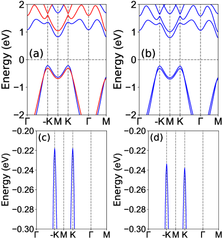
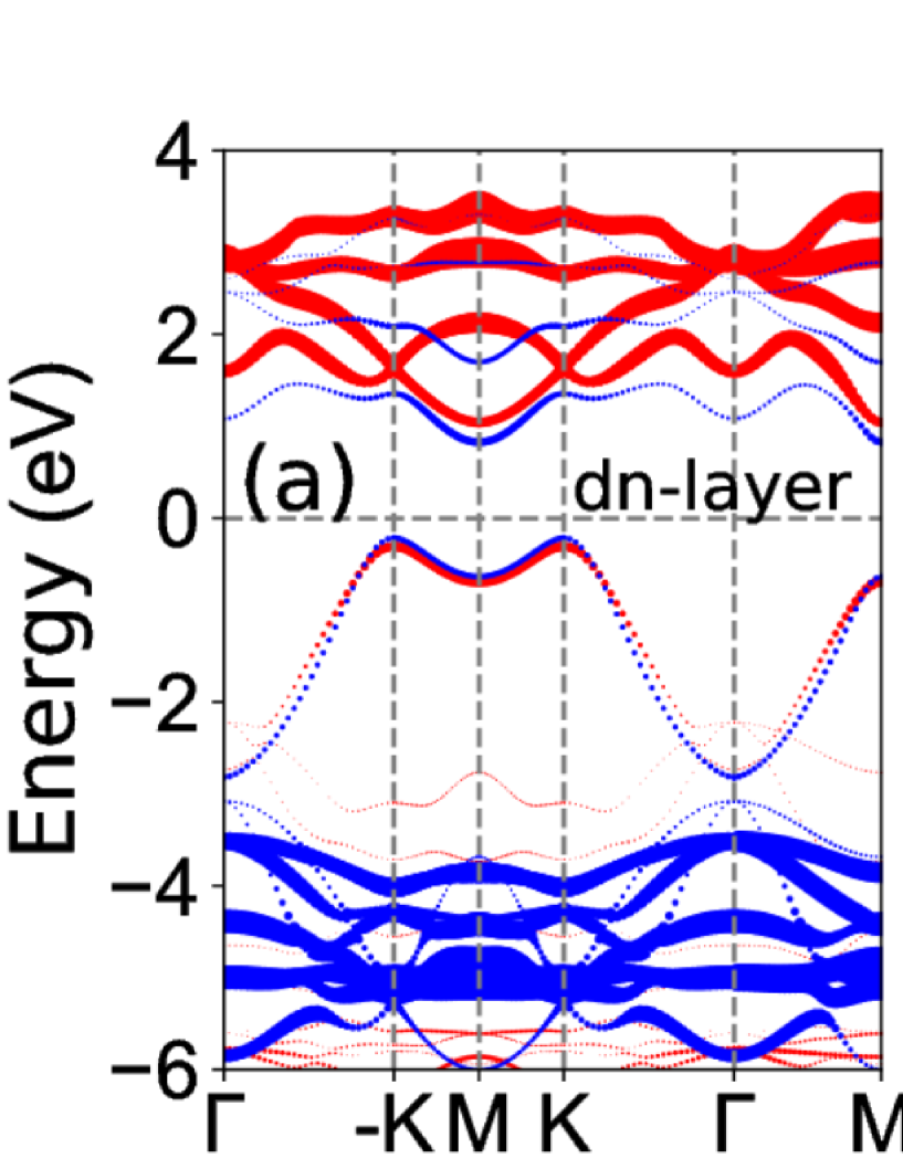
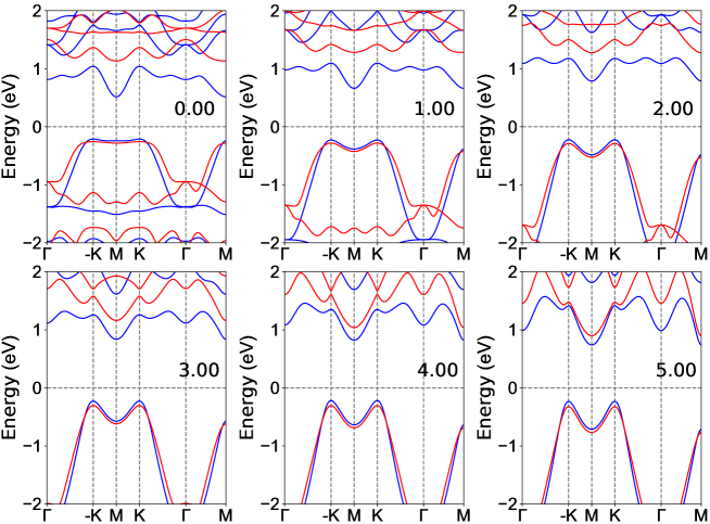
The magnetic moments of bottom and top Mn atoms are 4.57 and -4.52 , and total magnetic moment per unit cell is strictly 0.00 . In general, no spin splitting can be observed for AFM material. However, our proposed shows obvious spin splitting from calculated energy band structures without SOC in Figure 2 (a). This is very different from energy band structures of (see FIG.4 of ESI), where no spin splitting exists. This difference is because the possesses the out-of-plane polar electric field, while the built-in electric field of disappears. It is clearly seen that is an indirect band gap semiconductor with gap value of 1.043 eV. The valence band maximum (VBM) and conduction band bottom (CBM) are at high symmetry K/-K and M points, respectively, and they are provided by the same spin-up channel. When including the SOC, the energy band structures of have very small changes, and it is still an indirect bandgap semiconductor with reduced gap value of 1.028 eV (Figure 2 (b)). Without considering SOC, the K and -K valleys of valence bands are exactly degenerate (Figure 2 (c)). However, when SOC is switched on, the energy degeneracy between the K and - K valleys is lifted due to broken space- and time-inversion symmetries, leading to an interesting phenomenon of the spontaneous valley polarization with very small valley splitting of 4.3 meV (Figure 2 (d)). This is different from the common valley splitting in FM materialsduan . Recently, the spontaneous valley polarization is also predicted in 2D AFM with a valley splitting of 16.3 meVjmc . For , the layer-characters energy band structures without SOC and with SOC are plotted in Figure 3. Calculated results show that the weights of spin-up and spin-down of both valence and conduction bands are reversed in different Mn layers (Figure 3 (a) and (b)), which gives rise to the obvious spin splitting. According to Figure 3 (c), it is clearly seen that two Mn layers are non-equivalent due to a layer-dependent electrostatic potential caused by the built-in electric field.
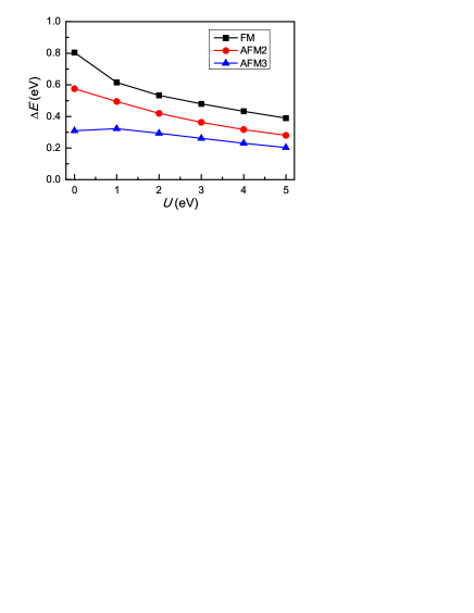
The electronic correlation can produce important effects on the magnetic ground state, electronic structures and topological properties of 2D magnetic materialsre1 ; re2 ; re3 ; re4 ; re5 . To confirm robust EPD-AFM, the electronic correlation effects on physical properties of are considered by using different values. Firstly, the lattice constants of are optimized by GGA+ (0-5 eV), and then calculate its related physical properties. Based on FIG.5 of ESI, the lattice constants (3.286 -3.447 ) increases with increasing . To achieve EPD-AFM, the AFM1 magnetic configuration as the ground state of is a crucial factor. So, the energy differences between FM/AFM2/AFM3 and AFM1 (per unit cell) as a function of are plotted in Figure 4. It is found that is always a AFM1 ground state in considered range. The evolutions of energy band structures as a function of are plotted in Figure 5, and the total gap vs is shown in FIG.6 of ESI. In considered range, the is always an indirect gap semiconductor, and shows obvious spin splitting. The VBM and CBM are always at high symmetry K/-K and M points, which are provided by the same spin-up channel. Finally, the MAE as a function of is plotted in FIG.7 of ESI. When is less than about 4.7 eV, the out-of-plane magnetic anisotropy can be maintained. These results show that the EPD-AFM of is robust.
V Piezoelectric properties
The monolayer possesses no piezoelectricity because of inversion symmetry. However, due to broken horizontal mirror symmetry, the monolayer has both in-plane and out-of-plane piezoelectricity. The piezoelectric response of a material can be described by the third-rank piezoelectric stress tensor and strain tensor , which can be expressed as the sum of ionic and electronic contributions:
| (4) |
In which , and are polarization vector, strain and stress, respectively. The superscripts / means electronic/ionic contribution. The and are called clamped-ion piezoelectric coefficients, while the and are called relaxed-ion piezoelectric coefficients. The is related with by elastic tensor :
| (5) |
By using Voigt notation, when only considering the in-plane strain and stressyd1 ; yd2 ; yd3 , the Equation 5 with symmetry can be reduced into:
| (6) |
With an imposed uniaxial in-plane strain, both in-plane and out-of-plane piezoelectric polarization can be produced (/0 and /0). However, when a biaxial in-plane strain is applied, the in-plane component will disappear(/=0), but the out-of-plane component still exists (/0). By solving the Equation 6, the two independent and can be derived:
| (7) |
The orthorhombic supercell (see Figure 1 (e)) as the computational unit cell is used to calculate the / of . The calculated / is -0.745/-0.191 C/m with ionic part -0.647/0.372 C/m and electronic part -0.098/-0.563 C/m. For , the same signs can be observed for the electronic and ionic contributions, and the ionic part plays a decisive role. However, for , the electronic and ionic contributions have opposite signs, and the electronic part dominates the piezoelectricity. Based on Equation 7, the calculated and of are -1.89 and -0.26 pm/V, respectively. The predicted is higher than or compared with those of other 2D known materialsyd1 ; yd2 ; yd3 , which provides possibility to tune spin splitting in by piezoelectric effect.
Electric-field induced spin splitting in has been confirmed by the first-principles calculationsk14 . The out-of-plane electric field can tune the spin splitting in . When a biaxial in-plane strain is imposed, only out-of-plane appears, and an out-of-plane electric field can be induced, which can be used to tune spin splitting in . Piezotronic effect on Rashba spin splitting in a ZnO/P3HT nanowire array structure has been studied experimentallyydt . It is found that the Rashba spin splitting can be effectively tuned by inner-crystal piezo-potential created inside the ZnO nanowires. So, the coupling between spin splitting and piezoelectric effect may be observed by EPD-AFM.
VI Discussion and Conclusion
For a 2D altermagnet, the magnetic atoms have opposite layer spin polarization (A-type AFM ordering). If the out-of-plane built-in electric field is lacking, the obvious spin splitting in the band structures can still be observed (Figure 6 (a) and (b)). However, the spin-valley polarization is lacking. Recently, this have been achieved in 2D yz . For a 2D Janus altermagnet, the magnetic configuration is still A-type AFM ordering, but it has an out-of-plane built-in electric field , which will produce spin-valley polarization(Figure 6 (c) and (d)). This is because a layer-dependent electrostatic potential makes electronic bands in different layers stagger, producing the spin-valley polarization. The out-of-plane polarization filed is equivalent to an external electric fieldar1 . By applying a gate field of 0.2 eV/, monolayer possesses a significant spin-valley splitting up to 123 meVyz . So, an out-of-plane built-in electric field can induce spin-valley polarization. The 2D Janus A-type altermagnetic material can be called electric-potential-difference altermagnet (EPD-AM).
In summary, we propose an alternative strategy to obtain spin splitting based on 2D Janus A-type antiferromagnet. It is demonstrated that 2D is a possible candidate for realizing EPD-AFM, which is dynamically, mechanically and thermally stable. It is proved that the EPD-AFM is robust against electron correlation in . The structural symmetry-breaking leads to out-of-plane piezoelectric response, providing a possibility to tune spin splitting in by piezoelectric effect. Our works reveal a new 2D family of AFM materials with spin splitting, which allow high-speed spintronic device applications.
Acknowledgements.
This work is supported by Natural Science Basis Research Plan in Shaanxi Province of China (2021JM-456). We are grateful to the China University of Mining and Technology (CUMT) for VASP software to accomplish this work. We are grateful to Shanxi Supercomputing Center of China, and the calculations were performed on TianHe-2.References
- (1) J. Nitta, T. Akazaki, H. Takayanagi, and T. Enoki, Phys. Rev. Lett. 78, 1335 (1997).
- (2) J. Nitta, T. Akazaki, H. Takayanagi and T. Enoki, Phys. Rev. Lett. 78, 1335 (1997).
- (3) A. Manchon, H. C. Koo, J. Nitta, S. M. Frolov and R. A. Duine, Nat. Mater. 14, 871 (2015).
- (4) E. I. Rashba, Sov. Phys. Solid State 2, 1224 (1960).
- (5) M. I. Dyakonov and V. I. Perel, Sov. Phys. Solid State 13, 3023 (1972).
- (6) B. A. Bernevig, J. Orenstein, and S.-C. Zhang, Phys. Rev. Lett. 97, 236601 (2006).
- (7) J. Schliemann, Rev. Mod. Phys. 89, 011001 (2017).
- (8) P. Altmann, M. P. Walser, C. Reichl, W. Wegscheider, and G. Salis, Phys. Rev. B 90, 201306(R) (2014).
- (9) X. Hu, Adv. Mater. 24, 294 (2012).
- (10) T. Jungwirth, J. Sinova, A. Manchon, X. Marti, J. Wunderlich and C. Felser, Nat. Phys. 14, 200 (2018).
- (11) L. mejkal, J. Sinova and T. Jungwirth, Phys. Rev. X 12, 031042 (2022).
- (12) I. Mazin Phys. Rev. X 12, 040002 (2022).
- (13) L. mejkal, J. Sinova and T. Jungwirth, Phys. Rev. X 12, 040501 (2022).
- (14) X. Chen, D. Wang, L. Y. Li and B. Sanyal, Preprint at https://arxiv.org/abs/2104.07390 (2021).
- (15) P. J. Guo, Z. X. Liu and Z. Y. Lu, npj Comput. Mater. 9, 70 (2023).
- (16) S. D. Guo, X. S. Guo, K. Cheng, K. Wang and Y. S. Ang, Preprint at https://doi.org/10.48550/arXiv.2306.04094 (2023).
- (17) H.-Y. Ma, M. L. Hu, N. N. Li, J. P. Liu, W. Yao, J. F. Jia and J. W. Liu, Nat. Commun. 12, 2846 (2021).
- (18) Y. J. Niu, H. F. Lv, X. J. Wu and J. L. Yang, J. Phys. Chem. Lett. 14, 4042 (2023).
- (19) P. Hohenberg and W. Kohn, Phys. Rev. 136, B864 (1964); W. Kohn and L. J. Sham, Phys. Rev. 140, A1133 (1965).
- (20) G. Kresse, J. Non-Cryst. Solids 193, 222 (1995).
- (21) G. Kresse and J. Furthmller, Comput. Mater. Sci. 6, 15 (1996).
- (22) G. Kresse and D. Joubert, Phys. Rev. B 59, 1758 (1999).
- (23) J. P. Perdew, K. Burke and M. Ernzerhof, Phys. Rev. Lett. 77, 3865 (1996).
- (24) Q. L. Sun and N. Kioussis, Phys. Rev. B 97, 094408 (2018).
- (25) C. Ma, X. J. Chen, K. J. Jin et al., J. Phys. Chem. Lett. 14, 825 (2023).
- (26) Q. Y. Ma, W. H. Wan, Y. M. Li and Y. Liu, Appl. Phys. Lett. 120, 112402 (2022).
- (27) X. Wu, D. Vanderbilt and D. R. Hamann, Phys. Rev. B 72, 035105 (2005).
- (28) A. Togo, F. Oba and I. Tanaka, Phys. Rev. B 78, 134106 (2008).
- (29) R. C. Andrew, R. E. Mapasha, A. M. Ukpong and N. Chetty, Phys. Rev. B 85, 125428 (2012).
- (30) W. Y. Tong, S. J. Gong, X. Wan, and C. G. Duan, Nat. Commun. 7, 13612 (2016).
- (31) P. Jiang, X. H. Zheng, L. L. Kang, X. X. Tao, H. M. Huang, X. C. Dong and Y. L. Li, J. Mater. Chem. C 11, 2703 (2023).
- (32) S. D. Guo, J. X. Zhu, M. Y. Yin and B. G. Liu, Phys. Rev. B 105, 104416 (2022).
- (33) S. D. Guo, W. Q. Mu and B. G. Liu, 2D Mater. 9, 035011 (2022).
- (34) S. D. Guo, Y. L. Tao, W. Q. Mu and B. G. Liu, Front. Phys. 18, 33304 (2023).
- (35) S. Li, Q. Q. Wang, C. M. Zhang, P. Guo and S. A. Yang, Phys. Rev. B 104, 085149 (2021).
- (36) W. Y. Pan, Phys. Rev. B 106, 125122 (2022).
- (37) L. Dong, J. Lou and V. B. Shenoy, ACS Nano, 11, 8242 (2017).
- (38) M. N. Blonsky, H. L. Zhuang, A. K. Singh and R. G. Hennig, ACS Nano 9, 9885 (2015).
- (39) K. N. Duerloo, M. T. Ong and E. J. Reed, J. Phys. Chem. Lett. 3, 2871 (2012).
- (40) L. Zhu, Y. Zhang, P. Lin et al., ACS Nano 12, 1811 (2018).
- (41) R. W. Zhang, C. X. Cui, R. Z. Li, J. Y. Duan, L. Li, Z. M. Yu and Y. G. Yao, Preprint at https://doi.org/10.48550/arXiv.2306.08902 (2023).
- (42) A. O. Fumega and J. L. Lado, Nanoscale 15, 2181 (2023).