DeePTB: A deep learning-based tight-binding approach with ab initio accuracy
Abstract
Simulating electronic behavior in materials and devices with realistic large system sizes remains a formidable task within the ab initio framework. We propose DeePTB, an efficient deep learning-based tight-binding (TB) approach with ab initio accuracy to address this issue. By training with ab initio eigenvalues, our method can efficiently predict TB Hamiltonians for unseen structures. This capability facilitates efficient simulation of large-size systems under external perturbations like strain, which are vital for semiconductor band gap engineering. Moreover, DeePTB, combined with molecular dynamics, can be used to perform efficient and accurate finite temperature simulations of both atomic and electronic behavior simultaneously. This is demonstrated by computing the temperature-dependent properties of a GaP system with atoms.
Despite much progress, the simulation of materials and devices with practically relevant system sizes still remains a significant challenge within the ab initio framework. For instance, obtaining accurate electronic structure information with computationally expensive hybrid functionals [1, 2] is crucial for band-gap engineering.However, at the moment, performing such calculations for realistic large-scale systems is quite infeasible. In addition, atomic vibration at finite temperatures is inevitable and often influences the electronic structure. Thermal-driven structural changes and insulator-to-metal phase transitions, with applications in areas like thermal sensors [3, 4], require comprehensive simulations that consider both atomic and electronic degrees of freedom. Furthermore, the computational demands associated with accessing accurate electronic Hamiltonians for quantum transport simulations [5, 6] on large systems are implausible within the current density functional theory (DFT) framework. Incorporating the effects of atomic vibrations in the investigation of temperature-dependent transport properties adds further complexity [7]. Such simulations are beyond the capabilities of ab initio approaches and hence often require simplified approaches that can bear the computational cost.
In this regard, the tight-binding (TB) method offers a more practical alternative for describing electronic Hamiltonians using smaller and more sparse matrices [8, 9]. Traditionally, TB Hamiltonians are constructed using empirical parameters [8, 10, 11], but their accuracy and transferability are often questioned. To address this issue, the ab initio approach has been developed to improve the accuracy and reliability of TB models [12, 13, 14, 15]. It involves the projection of self-consistent ab initio Hamiltonians onto localized bases formed by Wannier functions [12], quasi-atomic orbital [14, 15], etc. Although one gains accuracy, the construction of the Hamiltonian remains time-consuming due to the cost associated with the ab initio calculations and the projection step. Furthermore, the ab initio TB Hamiltonian obtained this way lacks transferability to new structural configurations, limiting its applicability for electronic simulations. Hence, a trade-off between accuracy and efficiency is inevitable in both the traditional and ab initio TB methods.
Several attempts have been made to address the dilemma of accuracy versus efficiency in modeling the electronic Hamiltonians using machine learning (ML) techniques. Some are designed to learn the electronic Hamiltonians for molecular systems [16, 17]. For solid systems, ML approaches have been proposed to learn the Kohn-Sham Hamiltonians [18, 19, 20] directly obtained from a specific DFT package based on the linear combination of atomic orbitals (LCAO) basis [21]. While learning the DFT Hamiltonian is straightforward, it is limited to working with only the LCAO DFT packages. It is also less efficient since they are usually larger and denser than the TB ones. Wang et. al. [22] designed the ML-based algorithms for generating TB matrices from electronic eigenvalues. However, no atomic structure information was considered in this case, prohibiting its transferability to “unseen” structures. A subset of the authors was involved in the TBworks [23] method, where TB Hamiltonians were constructed by learning the ab initio eigenvalues. This approach has only been applied to one-dimensional chains. Clearly, a more general ML-based approach is warranted to efficiently generate accurate and transferable TB Hamiltonians.
In this work, we propose a deep learning-based TB method, dubbed DeePTB hereafter, to efficiently represent the electronic structure of materials with ab initio accuracy. We adopt the Slater-Koster (SK) framework [8], where TB Hamiltonians are constructed using gauge-invariant parameters. DeePTB maps these parameters from symmetry-preserving local environment descriptors to obtain the TB Hamiltonian and its corresponding eigenvalues. This goes beyond the traditional two-center approximation in the empirical approaches. After supervised learning from training structures with ab initio eigenvalues, DeePTB can directly predict accurate TB Hamiltonians for unseen structures during the atomic structure explorations. We found that using eigenvalues as the training labels makes DeePTB much more flexible and independent of the choice of various bases and the form of the exchange-correlation (XC) functionals used in preparing the training labels. In addition, DeePTB can handle systems with strong spin-orbit coupling (SOC) effects.
Results
We now describe the main architecture and framework of DeePTB in great detail and demonstrate its capabilities in terms of accuracy, transferability, and flexibility. We use the group-IV elemental substances and III-V group compounds as test cases. Our choice of test materials is based on the fact that they are extensively utilized in various electronic devices. Our method is expected to be an accurate and efficient surrogate model of DFT and applicable to a wide range of materials. The capability of DeePTB in dealing with realistic large-scale and long-time material simulations is demonstrated by considering a cell of one million () atoms of gallium phosphide (GaP) system and calculating the electronic density of states (DOS), optical conductivity, dielectric function, and refractive index at finite temperatures. This further opens up previously inaccessible or challenging avenues of computational science research.
Theoretical framework of DeePTB. The TB Hamiltonian in DeePTB takes a simplified form of the full Kohn-Sham Hamiltonian [24] and is based on a minimal set of localized basis functions . is the site index at position . and are angular and magnetic quantum numbers, respectively. The elements of TB Hamiltonian matrices can be expressed as:
| (1) |
For , , and orbitals, () . () ranges from to . In this paper, we set the bases to be orthogonal. The parameterization of Hamiltonian elements in Eq. 1 takes the SK formulation [8]. As for the hopping elements (), it can be obtained as,
| (2) |
Here is the transformation matrix dependent solely on the direction cosines (where ) between the two sites and SK integrals are for -type bond. For instance, - SK integrals include and for and bonds respectively.
As for the on-site matrix (), a generalized strain-dependent onsite formalism by Niquet et. al. [25] is adopted in our work. This allows our model to simulate the strain effect,
| (3) |
Here, is the orbital energy. runs over all the neighbors of site within a cut-off radius. represents the SK-like integrals for the onsite matrix elements between the site and its neighbors. It is always possible to set all to zero, which returns to the onsite formalism of the original SK method [8].
Additionally, for the systems with non-negligible SOC effect (usually the case of heavy atoms), this effect must be considered, which can be formulated as [26],
| (4) |
Here, and are the orbital and spin momentum operators with interaction strength . The full Hamiltonian with SOC effect can be constructed as , where is the identity matrix and is the Kronecker product.
In short, as described in Eq.(2-4), to construct the TB Hamiltonians, one needs to define the bond-wise parameters, i.e. and , as well as the atomic parameters including and . It is worth noting that in the empirical TB approach, the SK integrals are obtained based on the two-center approximation and depend only on the relative separation of the two centers, while the atomic parameters depend only on the nature of the atomic species. Within DeePTB, the TB parameters have not only analytical bond length dependence but also local environment-dependent corrections from neural networks. Hence, our approach is highly expressive and goes beyond the two-center approximation. The detailed NN architecture will be discussed next.
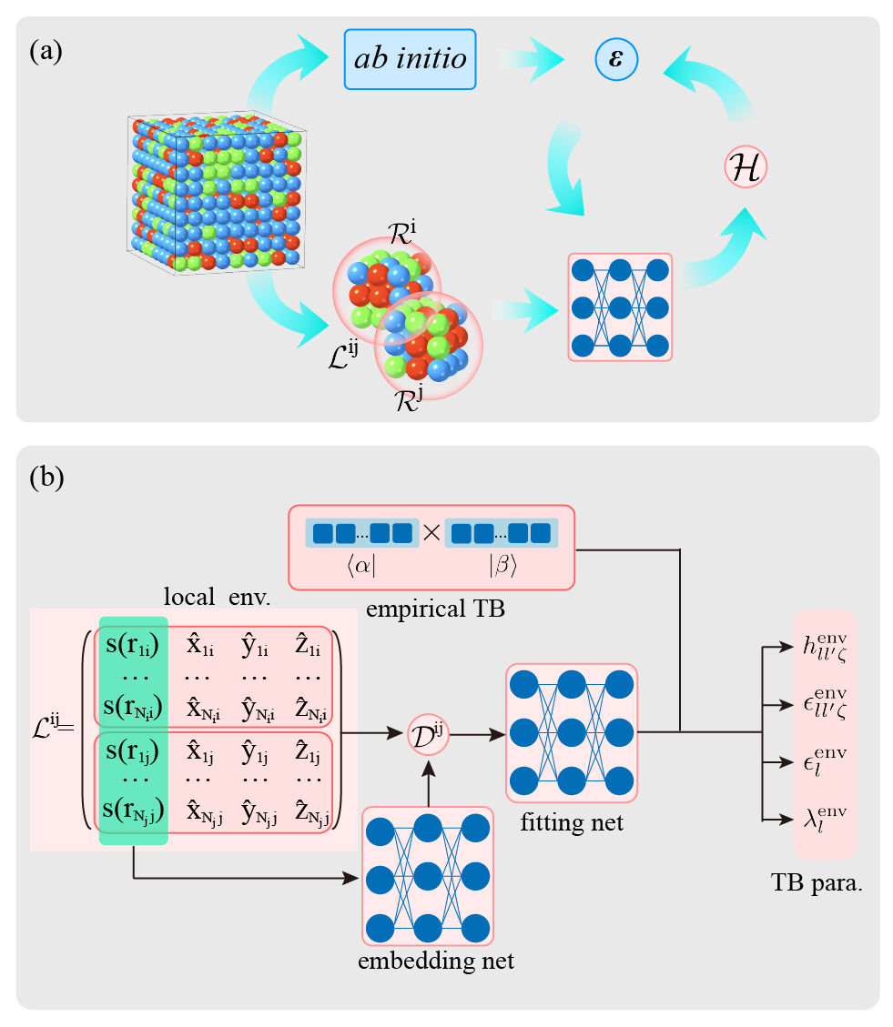
Neural network architecture of DeePTB. The general architecture of DeePTB is presented in Figure 1. The DeePTB broadly involves a three-step process. We first construct an empirical TB Hamiltonian for a system described by structure . Then in the second step, DeePTB extracts the local chemical environments, which are subsequently utilized to construct symmetry-preserving environment descriptors. These descriptors are then fed into the NN to obtain the environment-dependent TB parameters. In the third and final step, we train our NN model with the ab initio electronic bands as the target. Here, are the band and lattice momentum indices respectively. Formally, these parameters can be represented as,
| (5) |
For brevity, we only present the SK hopping integrals as an example. Here is the bond length as described earlier and is the local environment descriptor of bond-. Descriptors are invariant under the translational, permutational, and rotational symmetry operations. maps the and to correct the empirical parameters to provide the environment-based . is the atomic orbital on atom . Other parameters can be obtained in a similar fashion, that is using environment descriptors for the correction of empirical parameters. We now introduce the details of each term in Eq.(5).
For the empirical TB parameters terms, they are defined as analytical functions of the bond length with several coefficients to be fitted, such as the power-law formula defined in Ref. [8, 11]. For each coefficient, we generate two vectors by sets of neurons, and represent them by the inner product . This way, the empirical parameters, which give a good start for the environment corrections, can be fitted efficiently with NN-based optimization when trained on the ab initio band structures.
The local environment descriptors are constructed from the local chemical environment of each site. For site-, its local chemical environment can be defined as a tensor ,
| (6) |
where is the index of neighboring the atoms lying within a sphere of radius centered at . is the total number of and is a smooth function of the scalars . The environment descriptor , inspired by DeepPot-SE model [27], is constructed from and . Here, we define bond-environment matrix as as shown in Fig. 1(b), containing the information of atomic positions. Similarly, we can define an embedding matrix , where each contains the embeddings of . is mapped by a embedding neural network . Here denotes the chemical species of atom-. Finally, the descriptor of bond- is constructed as,
| (7) |
where takes only columns of , to reduce the size of descriptors. Descriptors are proved to be invariant to the translational, permutational, and rotational symmetry operations. The invariance under the interchange of two center atoms to is automatically guaranteed in . Therefore, only the bonds- with need to be calculated.
The embedding neural network is a function that maps the radial information of each bond to an embedding vector. The vectors are later used to construct the environmental descriptors. The fitting network takes environmental descriptors as input and generates TB parameters as output. and is composed of multiple layers of standard fully connected NN with optional residual connections [28]. The fully connected NN is composed of a series of linear transformations and nonlinear activation functions. Formally, each layer is expressed as where is weighted by a matrix and biased by a vector . It is then fed into the non-linear function ( in our settings). When with residual connections, the output of layer is added with an identity mapping, giving as the layer output. We employ up or downsampling techniques when the input and output dimensions mismatch.
In the last step, the obtained parameters are then transformed to the Hamiltonian matrix as defined in Eq. 2-3. It finally leads to the environment-dependent TB Hamiltonian , which is exactly diagonalized to obtain the eigenvalues. The embedding and fitting NNs are trained by minimizing the loss function defined as:
| (8) |
Here, the and are the eigenvalues from the predicted TB Hamiltonian and ab initio calculations, respectively. Depending on the choice of TB basis set, the is chosen from the low energy subspace of the full KS eigenvalues. The eigenvalues are sorted by their magnitude, determining the order of band-, which is weighted by user-defined weights . is the difference of the eigenvalues between and a randomly chosen . In the training process, optimization algorithms such as Adam [29] are available for the optimal parameters. The detailed training process is described in the Method section. Next, we proceed to showcase the performance and abilities of our DeePTB approach, considering various materials from IV and III-V groups as examples.
Validation on MD trajectories.
We demonstrate the generalization ability of DeePTB to accurately predict TB Hamiltonians for unseen snapshots in MD trajectories. This ability is particularly valuable for electronic simulations, where the dynamic effects and interplay of ionic and electronic degrees of freedom are crucial. We present the test results in predicting TB Hamiltonians for unseen configurations from MD trajectories of 4 group-IV systems including diamond (C), silicon (Si), germanium (Ge), and alpha-tin (-Sn), as well as 12 compounds formed by group-III elements (aluminum (Al), gallium (Ga) and indium (In)) and group-V elements (nitrogen (N), phosphorus (P), arsenic (As) and antimony (Sb)). For the group-IV systems, we focused on their cubic phase, specifically the diamond structure, as it is the most thermodynamically stable under standard conditions. Regarding the III-V group systems, we considered both the cubic phase (zincblende structure) and the hexagonal phase (wurtzite structure). This distinction is necessary because certain III-V materials are stabilized in the hexagonal phase, while others exhibit the cubic phase.
The NVT ensemble MD simulations are performed by LAMMPS package [30] using the Tersoff potential [31, 32] at a temperature K with Nose-Hoover thermostat [33, 34]. Each material was simulated within the conventional unit cell for a duration of 500 picoseconds (ps). Throughout the MD simulations, structure snapshots were saved every 500 femtoseconds (fs) to eliminate correlations between adjacent structures for subsequent training and testing. The obtained structure snapshots were then used to calculate the ab initio eigenvalues using the ABACUS package [35, 36]. In these DFT calculations, we employed the double-zeta polarization (DZP) basis set and norm-conserving Vanderbilt type (ONCV) [37] Perdew-Burke-Ernzerhof (PBE) [38] functional. We select the first 100 snapshots of structures in each MD trajectory as the training and the last 500 snapshots as the testing data set. This choice minimizes the correlations between the training and testing data, thereby providing a robust assessment of the predictive power of our DeePTB model. More details about the MD simulations and DFT calculations can be found in the Method section.
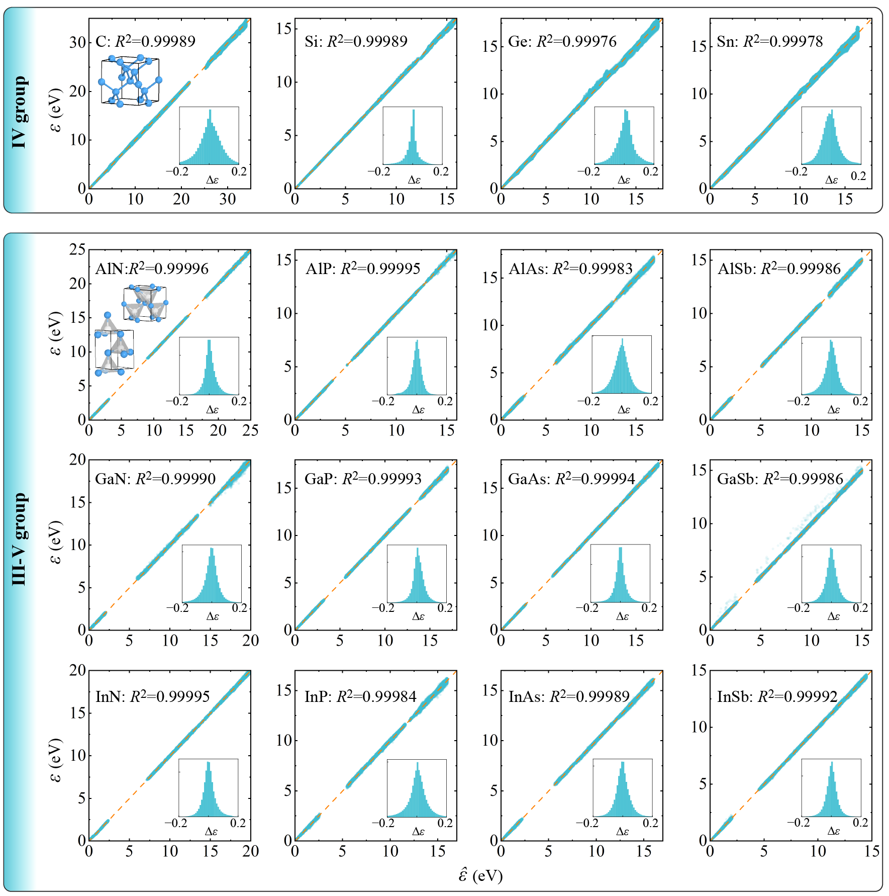
To accurately represent the ab initio eigenvalues from low energy subspace, DeePTB utilizes a minimal set of orbitals as the basis and incorporates hoppings up to the third nearest neighbors in the TB Hamiltonians. For the local environment, the cut-off radius is also set to include 3rd nearest neighbors. For instance, in the case of Si Å. The DeePTB models are initially trained on the primitive unit cell to get a starting point for training on the MD-simulated configurations. Once training converges, the DeePTB models are employed to predict the TB Hamiltonians for unseen structures in the testing data. The accuracy of the predicted Hamiltonians is assessed by comparing their eigenvalues with their ab initio counterparts. The upper panel of Fig. 2 shows a parity plot comparing the DeePTB-predicted and ab initio eigenvalues for structures of the group-IV materials, namely C, Si, Ge, and -Sn in the cubic phase. The ideal crystal structure is shown in the inset of the plot for the C system and Fig.S1 in Supplementary Materials (SM). The MD trajectories include distorted structures with bond length variations of approximately 10% around the ensemble-averaged value, as depicted in Figure S2 in the SM. The parity plots in Fig. 2 for the group-IV systems exhibit an exceptional agreement, as indicated by the coefficient of determination of 0.9999. Furthermore, the mean absolute errors (MAE) for all the group-IV systems are 40 meV, as presented in Table S1. These low MAE values further reinforce the high accuracy achieved by our method. Additionally, Fig. S3 in the SM demonstrates that the DeePTB models successfully reproduce the primitive band structures of the group-IV systems. All these results clearly indicate that our DeePTB models accurately captured the underlying microscopic physics and relationships between the structural and ab initio eigenvalues from training data.
As for III-V group systems, the ideal zincblende and wurtzite structures are shown in the inset of the plot for AlN in Fig. 2 and Fig.S1 in SM. Despite their similar local tetrahedral structure in both phases, their band structures differ due to distinct lattice symmetries. It poses challenges for the transferability of cubic 1st nearest neighbor empirical TB models to hexagonal structures, calling for separate parameterizations or more sophisticated models for different phases. Considering this particular case, we demonstrate the capability of our DeePTB model which can handle both cubic and hexagonal phases simultaneously. We start with training and testing our accurate model only on the cubic () phase with MAE of about 20 30 meV, as shown in the column of Table S1 in SM. Subsequently, we utilized the cubic DeePTB models as a starting point and trained them further on mixed () data from both cubic and hexagonal () phases. The resulting MAE values of the obtained DeePTB models for both phases range approximately meV, as one can see in the detailed values in Table S1 in SM. The lower panel of Fig. 2 illustrates the predicted eigenvalues against their ab initio counterparts for structures from both phases, exhibiting 0.9999. This confirms the high accuracy and reliability of our DeePTB model in capturing the underlying physics and accurately predicting eigenvalues for structures in both cubic and hexagonal phases. Additionally, Figures S3 and S4 in the SM demonstrate that the DeePTB model faithfully reproduces the primitive band structures of both phases, further affirming its fidelity and competence. To summarize this part, we demonstrated the high competence and versatility of the DeePTB approach in predicting electronic structures of different phases.
Validation on the larger-size and strained structures. Above, we explored the generalization capability of the DeePTB approach to unseen structures of the same size as the training set. The design of TB parameters in the DeePTB architecture, which depend on the local environment, enables its straightforward transferability to larger-size structures.
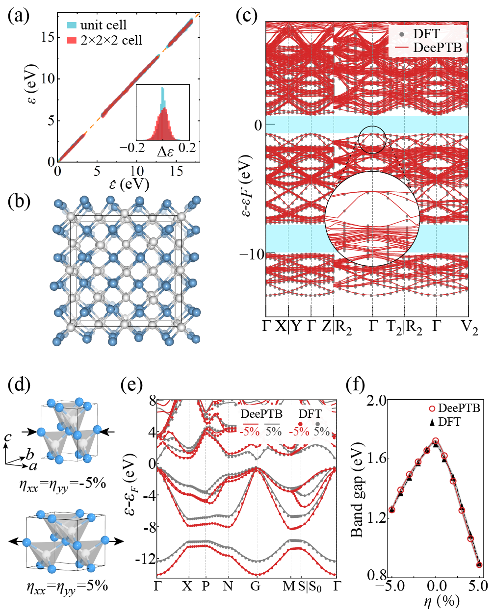
To demonstrate this generalization to larger-size structures, we consider the example of cubic GaP. We extract 500 testing structure snapshots from the MD trajectory of a supercell simulation box under the NVT ensemble at a temperature of K. This supercell dataset is then used to validate the DeePTB model, which was previously trained on the conventional smaller unit cell. The eigenvalues obtained from DeePTB and ab initio calculations for the supercell structures are plotted on top of the conventional unit cell in Fig. 3(a). Clearly, the DeePTB model exhibits excellent agreement with ab initio eigenvalues in both cases. In the supercell case, the and testing MAE is 26 meV, which is only slightly larger than meV achieved in the conventional unit cell case. Fig. 3(b) displays a distorted structure from the testing data, where the bond length varies up to 10% w.r.t. the undistorted ideal structure. Its complex ab initio band structure is well reproduced by the DeePTB as shown in Fig. 3(c). In particular, the separation of 2.4 eV and band gap 1.5 eV as indicated by the shaded regions are also well reproduced. These results highlight the strength of the DeePTB approach in terms of its transferability to larger-size structures.
In many cases, particularly for tuning electronic band structures and carrier mobility [39, 40], one often relies on strain engineering. However, the underline physical changes with strain can not be straightforwardly predicted. To account for strain effects, we incorporated an on-site correction term (Eq. (3)) and also introduced the local environment within our DeePTB framework. Here, considering the example of cubic GaP, we further demonstrate the performance of DeePTB on strained structures. We apply the biaxial stress perpendicular to the direction. Owing to the orthogonal lattice vectors of GaP, only non-zero strain tensor elements are and . Fixing , we get the strained lattice structures as illustrated in Figure 3(d). We set to vary from to , incorporating relatively large deformations that may exceed the elastic limit of materials. The DeePTB model was then further trained and validated on the strained configurations. As an explicit example, Fig. 3(e) displays the comparison between the DeePTB predicted and ab initio band structures for . One can see the excellent agreement between these two band structures. Additionally, Fig. 3(f) demonstrates that the band gaps for all strained cases (), are accurately reproduced by our DeePTB model, with a mean absolute error (MAE) of 26 meV. These results illustrate that the DeePTB model can successfully be generalized to larger-size structures as well as accurately capture the lattice strain effects on the electronic band structure.
Flexibility to different bases, XC functionals, and SOC effect. Previously, we employed the LCAO basis set and PBE functional for generating training eigenvalues. However, it is widely recognized that the accuracy and efficiency of DFT calculations depend on several factors, such as the choice of basis sets, XC functionals, and the inclusion of SOC effects. Unlike the approaches that directly learn DFT Kohn-Sham Hamiltonians only on the LCAO basis, DeePTB offers the advantage of being independent of such choices. To illustrate this flexibility, we consider GaAs as an example. The example of Si is shown in Fig.S5 in SM.
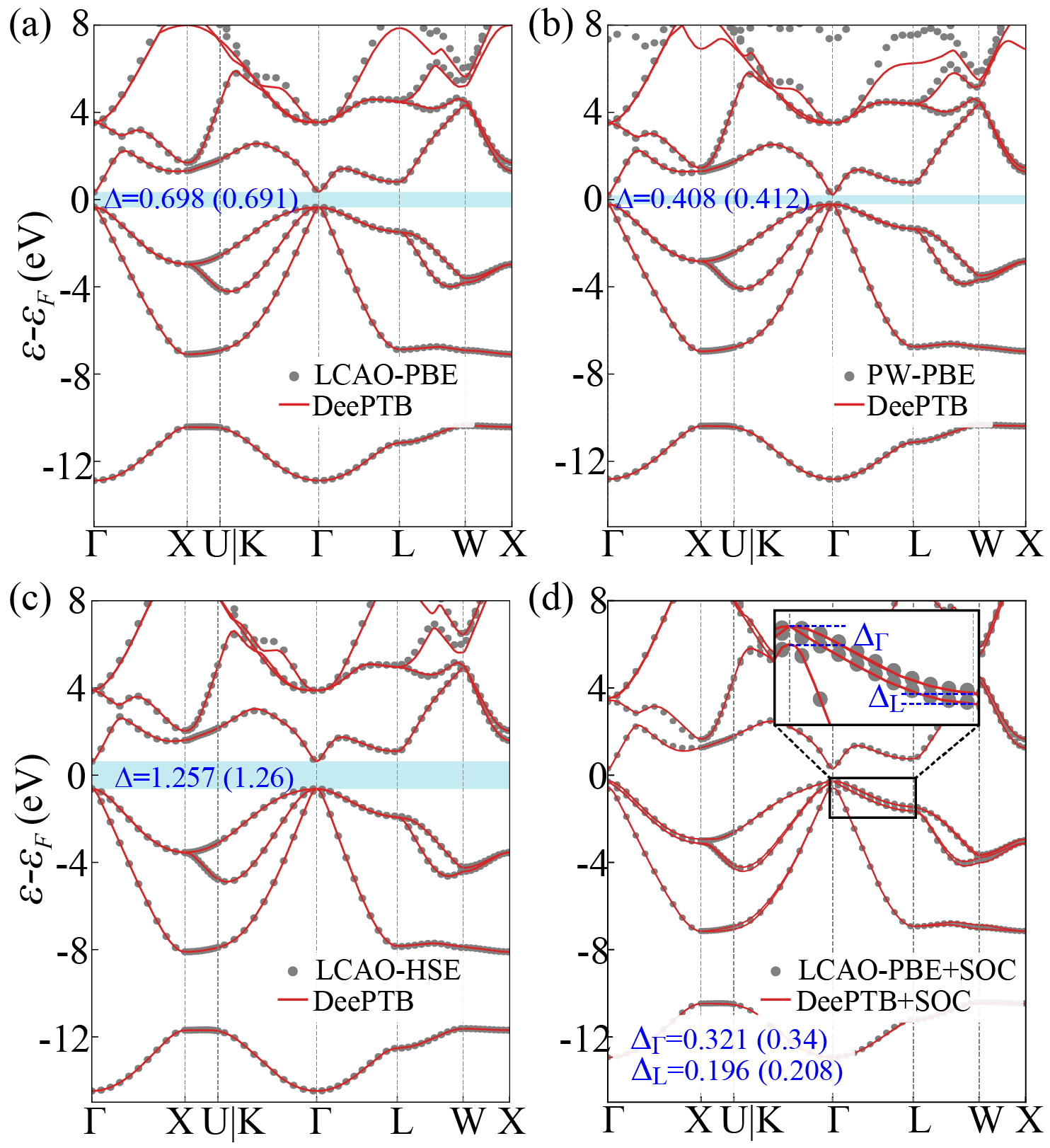
Fig. 4 showcases the DeePTB representation of DFT band structures calculated with different basis sets (LCAO and PW bases) and XC functionals (PBE and Heyd-Scuseria-Ernzerhof (HSE) hybrid functional) and the exclusion/inclusion of SOC effects. In the case of basis sets, we compare the LCAO and PW representations of GaAs band structures using the same PBE functional. Fig. 4(a)(b) showcase the DeePTB representation of ab initio band structures for these different basis sets. We utilize a DZP orbital within the LCAO basis and a plane wave cutoff of 100 Ry for the PW basis. Remarkably, despite the differences in the basis sets, the DeePTB accurately reproduces the subtle variations in the band structures. Furthermore, we investigate the impact of different XC functionals within the LCAO basis. Fig. 4(a)(c) illustrate the DeePTB band structures for GaAs calculated with the PBE and HSE functionals. The PBE functional tends to underestimate the band gap, resulting in a value of 0.691 eV for GaAs. In contrast, the HSE functional provides a more accurate band gap of 1.26 eV, much closer to the experimental value of 1.52 eV. The DeePTB approach exhibits the ability to accurately capture the dispersion and the distinct band gaps for both XC functionals.
As for the SOC effect, which is known to be significant for heavy atoms, we consider the cases of excluding/including SOC effects of GaAs system using the same basis and XC functionals as shown in Fig. 4(a)(d). Please refer to Fig.S6 for the cases of Sn and InSb. Fig.4(a)(d) demonstrates that the DeePTB band structures of GaAs agree well with the DFT-calculated ones, both with and without considering the SOC effect. The SOC effect leads to the splitting of certain energy bands, as shown in Fig.4(d). The energy splitting is most pronounced along the path, with a splitting magnitude of eV and eV at the and points, respectively. These splittings are accurately captured by DeePTB. The inset of Fig. 4(d) provides a zoomed-in view of the two split bands along the path.
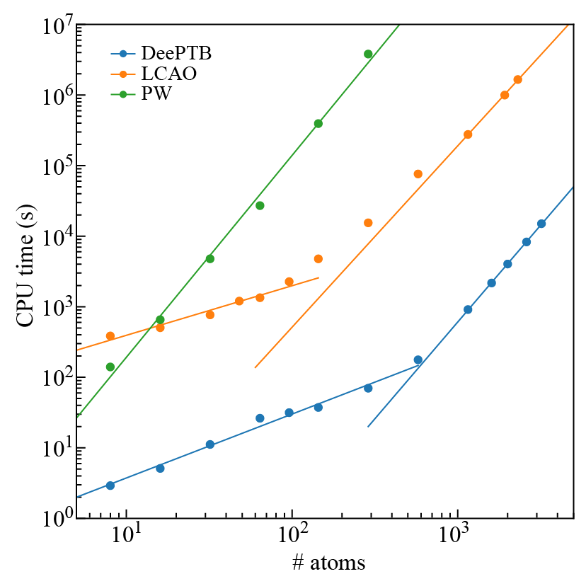
Computational efficiency In the case of computational simulations on large-size systems, one often has to choose between the computational cost and the accuracy of calculations. With DeePTB we intend to overcome this computational bottleneck. Having shown the accuracy being the ab initio level, we now demonstrate the high efficiency of our DeePTB approach. For this purpose, we compare the CPU time costs for computing the electronic eigenvalues in DeePTB and that from the ab initio calculations with PBE functionals. We again consider DZP orbital for LCAO basis, 100 Ry for energy cutoff in PW basis. The CPU times are obtained on a computing node equipped with Intel(R) Xeon(R) Platinum 8163 CPU @ 2.50GHz (64 cores). As shown in Fig. 5, for smaller-size systems, both our DeePTB and LCAO ab initio approach scale linearly with the number of atoms . This is primarily because, for smaller-sized systems, the majority of computational costs are expended on the Hamiltonian construction procedure. At this stage, the CPU times used by DeePTB are 2 orders of magnitude smaller than that of LCAO ab initio calculations. For system size larger than , where the diagonalization procedure takes the central stage in terms of computational cost, both the DeePTB and LCAO ab initio calculations scale roughly . Here, DeePTB has the advantage of being 3 orders faster than LCAO calculations in CPU times. As for the PW case, it exhibits a cubic scaling behavior for all the system sizes. For the larger-size systems, DeePTB is highly efficient with 5 order of magnitude faster than PW calculations in terms of CPU time. This indicates that DeePTB provides a dramatic speedup in the simulation of electronic properties making it accessible to larger system sizes.
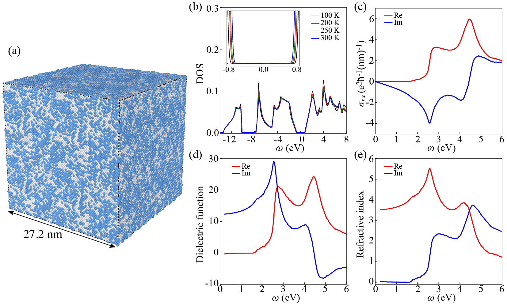
Application to one million atoms Now that we have demonstrated the efficiency and capabilities of DeePTB, we will showcase its ability to simulate finite temperature electronic properties using an example of cubic phase GaP. To this end, we consider a large system with dimensions of conventional supercell containing atoms ( orbitals), resulting in a simulation box with a length of approximately 27.2 nm, as illustrated in Fig. 6(a). In such a case, the evolution and sampling of ionic configurations are performed using deep potential MD simulations powered by DeePMD-kit package [41, 27]. Subsequently, DeePTB is utilized to predict the TB Hamiltonians for the structures from the obtained ionic trajectories. These Hamiltonians are then post-processed to explore electronic properties using the TB propagation method (TBPM) [42, 43] implemented in the TBPLaS package [44].
In our first demonstration, we computed the temperature-dependent electronic DOS. For a given instantaneous ionic structure , the corresponding electronic DOS can be calculated using time correlation function as,
Here, represents the correlation function for the ionic configuration . denotes the time-dependent wave function, where is the Hamiltonian operator and is the reduced Planck’s constant. By averaging over the MD trajectory, the temperature-dependent DOS can be obtained as , where the ionic dynamical effects on the electronic structure are intrinsically incorporated. Thanks to the sparsity of our DeePTB Hamiltonians, the time evolution operator can be efficiently applied to wave functions. This in turn guarantees a significant reduction in computational complexity from to nearly for systems with -atoms. This advantage is particularly valuable when dealing with large-scale systems. The temperature-dependent DOS is presented in Fig.6(b). Consistent with our expectation for a semiconductor, the band gap decreases as temperature increases, as illustrated in the inset of Fig.6(b).
To substantiate our claim about the application of DeePTB, we further calculated the electronic response properties, which include optical conductivity, dielectric function, and refractive index. Optical conductivity, a response of the induced current density in a material to an applied optical electric field of frequency , can be calculated using the Kubo formula [45] as follows,
Here, represents the volume of the system, denotes the current density operator, and represents the Fermi-Dirac distribution. Within the TBPM method, the current-current correlation enables the efficient computation of the real part of optical conductivity, denoted as . The imaginary part, , can be extracted using the Kramers-Kronig relation. Fig. 6(c) illustrates both the and in the energy range (0 – 6 eV). Notably, exhibits an onset threshold corresponding to the optical band gap value at eV. After the onset threshold, increases within the energy range of 1.5 to 4.5 eV, exhibiting two peaks at 2.8 and 4.5 eV with the maximum value of at 4.5 eV. From the obtained optical conductivity, we can straightforwardly derive the dielectric function as , where represents the vacuum permittivity. Similarly, the refractive index can be obtained from the dielectric function. Plots of the dielectric function and refractive index are shown in Figure 6(d) and (e), respectively. Our findings are in accordance with previous available theoretical and experimental studies [46, 47, 48]. A slight discrepancy in the peak positions may arise from the fact that exchange-correlation functionals, such as GGA, which were used to train our DeePTB model, tend to underestimate the electronic band gap of semiconductor materials.
Summary and discussion
In this work, we have introduced DeePTB, a general deep-learning-based TB approach, for predicting electronic Hamiltonians with ab initio accuracy. DeePTB is designed to be independent of the choice of the basis sets and the XC functionals for generating training labels, as well as the additional capability of handling the SOC effect. The most compelling aspect of DeePTB is its ability to sample various electronic properties during the structural configuration simulations, and the ability to explicitly consider the effects of external perturbations like strain. We demonstrated the capabilities of DeePTB by considering the examples of III-V and IV group materials. By considering a very large GaP system of atoms, we substantiate our claim about the power of DeePTB by calculating temperature-dependent properties such as DOS, optical conductivity, dielectric function, and refractive index.
A few remarks about the potential of the DeePTB framework are in order. For different XC functionals, the dispersive features of the band structures are more or less the same. Therefore, one may, in principle, first train the model on computationally efficient XC functionals like LDA or GGA, and further transfer it to more costly and accurate functionals like SCAN or HSE. This enables the highly accurate description of experimentally observable quantities for large-scale simulations needed in cases like material simulations that are close to reality. Also, for large-scale samples, simulations of strain effects on electronic properties are computationally cumbersome tasks. DeePTB can accelerate these simulations efficiently by training the model on smaller samples and transferring it to larger systems. This leads to advantages in the theoretical study of strain engineering on electronic structures. MD can provide the simulation of the ionic degree of freedom, that is analogous to the temperature probes of crystal structures, where ionic vibrations are a ground reality. DeePTB can be applied to simulate the temperature and structure-dependent electronic properties in cases where large-scale and long-time simulations are needed. Large-scale DeePTB simulations of electronic Hamiltonian can be used to perform quantum transport simulation using techniques like NEGF. DeePTB makes it possible and feasible to consider other practical scenarios like defects or impurities and their influence on the electronic structure. Another direction for DeePTB to explore is the simulation of the properties of magnetic systems. Given these diverse potential applications of DeePTB, we are confident that it can have far-reaching implications in the arena of electronic simulations.
Methods
Structure data preparation The test materials contain the cubic phase group-IV systems and both cubic and hexagonal phase for III-V systems. We performed the MD simulations at NVT ensemble using LAMMPS [30] package based on the Tersoff force-field [31, 32] to generate the distorted structures for training and testing. The simulation boxes are set to be the conventional unit cell, which is large enough to 3rd the nearest independent neighbors for the local environment. The lattice structures are shown in Fig. S1. For all the MD simulations, the temperature is set to be K using the Nose-Hoover thermostat [33, 34]. The simulation runs for 550000 MD steps (550 ps) with a time step of 0.001 fs. The first 50 ps of simulations are thermalization. We take the snapshot configurations every 0.5 ps to get 1000 snapshots for each phase of the materials. We randomly select 100 configurations from the first 500 structures as the training set, while the rest 500 is used as the testing set to minimize the correlations between the training and testing data. In order to test the generalization ability of DeePTB to a larger size, MD simulations on of conventional supercell of the GaP system are performed for further testing.
Electronic eigenvalues preparation The electronic eigenvalues data are obtained by the ab initio calculations using the atomic-orbital based ABACUS package [35, 36]. The DFT calculations are performed using LCAO bases formed by DZP orbitals with the Perdew-Burke-Ernzerhof (PBE) functional [38] and the SG15 Optimized Norm-Conserving Vanderbilt (ONCV) pseudopotentials [37]. To demonstrate the flexibility of DeePTB with various choices of basis sets and XC functionals, we perform the DFT calculations for testing data with different basis sets (LCAO and PW bases) and XC functionals (PBE, and HSE hybrid functional). In this case, We also consider DZP orbital within the LCAO basis, while for the PW basis, an energy cutoff of 100 Ry is used for the plane waves. In the case of SOC calculations, the fully-relativistic ONCV pseudopotentials are employed. In the self-consistent calculations, -mesh is taken as for the conventional unit cell and for the supercell. The convergence threshold is set to be for the charge density error between two sequential iterations. The band structures are then calculated along the high-symmetry paths. After the DFT calculation, the valence bands and lower energy conduction bands are picked out, whereas the high energy empty bands and core eleven bands are ignored in the TB models.
Training process The training consists of two sub-steps. First, the empirical TB parameters are initialized and trained. Here, we emphasize that the best way forward to start training is by first considering the minimal basis sets and nearest bond neighbors, which provides a rough estimation of the TB parameters. This step is physically meaningful, as it is the general scenario in solid systems where the first neighbor hoppings are the strongest. We use the minimal basis sets initially, mainly to obtain the simplest TB Hamiltonian and simultaneously to prohibit overfitting of the parameters. Then, our framework supports adding more neighbors and bases in subsequent steps and features like strain corrections and SOC effects. In the second step, we turn on the environment correction in DeePTB, which is then trained on samples from perturbed structures or MD trajectories to learn the environment dependency. The converged model can predict the TB Hamiltonians of new structures, which can generalize to systems with different sizes and local distortions.
DeePMD simulations The deep potential MD simulations were performed using the LAMMPS [30] package, employing a deep learning interatomic potential (DP) model provided by DeePMD-kit [41, 27]. The DP model was trained using the concurrent learning scheme implemented in the Deep-Potential Generator (DP-GEN). The training data set consisted of DFT calculations from the ABACUS package, employing TZDP basis sets and the PBE functional. The DP model achieves the accuracy of a root mean square error (RMSE) value of eV/atom for predicting the total energy and eV/Å for predicting forces. Using the DP model, MD simulations were performed at different temperatures for 100 ps on a supercell with dimensions of , containing atoms to generate the sampling of structures for temperature-dependent electronic properties calculations.
TBPM calculations The TBPM [42, 43] calculations were performed using the TBPLaS package [44] utilizing the DeePTB Hamiltonian to obtain electronic properties for large-size supercells of the GaP system. The supercell structures were constructed by enlarging snapshots obtained from DeePMD simulations to a supercell, containing a total of atoms. In TBPM, to evaluate the various time correlation functions, the random state wave functions are propagated a total of 2048 steps with a time-step of 0.105 . Due to the large-size structure, only one random state sample is used to obtain the electronic properties of each structure.
Acknowledgements.
Q. G. gratefully acknowledges fruitful discussions about the TBPLaS package with Prof. Shengjun Yuan and thanks Jianchuan Liu for providing the DP model for GaP system. We acknowledge the support of computing resources provided by the Bohrium Cloud Platform (https://bohrium.dp.tech) from DP TechnologyReferences
- Becke [1993] A. D. Becke, A new mixing of Hartree–Fock and local density‐functional theories, J. Chem. Phys. 98, 1372 (1993).
- Heyd et al. [2003] J. Heyd, G. E. Scuseria, and M. Ernzerhof, Hybrid functionals based on a screened Coulomb potential, J. Chem. Phys. 118, 8207 (2003).
- Kim et al. [2007] B.-J. Kim, Y. W. Lee, B.-G. Chae, S. J. Yun, S.-Y. Oh, H.-T. Kim, and Y.-S. Lim, Temperature dependence of the first-order metal-insulator transition in VO2 and programmable critical temperature sensor, Appl. Phys. Lett. 90, 023515 (2007).
- Strelcov et al. [2009] E. Strelcov, Y. Lilach, and A. Kolmakov, Gas Sensor Based on Metal-Insulator Transition in VO2 Nanowire Thermistor, Nano Letters 9, 2322 (2009).
- Brandbyge et al. [2002] M. Brandbyge, J.-L. Mozos, P. Ordejón, J. Taylor, and K. Stokbro, Density-functional method for nonequilibrium electron transport, Phys. Rev. B 65, 165401 (2002).
- Louis et al. [2003] E. Louis, J. A. Vergés, J. J. Palacios, A. J. Pérez-Jiménez, and E. SanFabián, Implementing the keldysh formalism into ab initio methods for the calculation of quantum transport: Application to metallic nanocontacts, Phys. Rev. B 67, 155321 (2003).
- Liu et al. [2015] Y. Liu, Z. Yuan, R. J. H. Wesselink, A. A. Starikov, M. Van Schilfgaarde, and P. J. Kelly, Direct method for calculating temperature-dependent transport properties, Phys. Rev. B 91, 220405 (2015).
- Slater and Koster [1954] J. C. Slater and G. F. Koster, Simplified LCAO method for the periodic potential problem, Phys. Rev. 94, 1498 (1954).
- Goringe et al. [1997] C. M. Goringe, D. R. Bowler, and E. Hernández, Tight-binding modelling of materials, Rep. Prog. Phys. 60, 1447 (1997).
- Goodwin et al. [1989] L. Goodwin, A. J. Skinner, and D. G. Pettifor, Generating transferable tight-binding parameters: Application to silicon, Europhysics Letters 9, 701 (1989).
- Harrison [1989] W. A. Harrison, Electronic Structure and the Properties of Solids: The Physics of the Chemical Bond (Dover Publications Inc., 1989).
- Marzari et al. [2012] N. Marzari, A. A. Mostofi, J. R. Yates, I. Souza, and D. Vanderbilt, Maximally localized Wannier functions: Theory and applications, Rev. Mod. Phys. 84, 1419 (2012).
- Andersen and Saha-Dasgupta [2000] O. K. Andersen and T. Saha-Dasgupta, Muffin-tin orbitals of arbitrary order, Phys. Rev. B 62, R16219 (2000).
- Lu et al. [2004] W. C. Lu, C. Z. Wang, T. L. Chan, K. Ruedenberg, and K. M. Ho, Representation of electronic structures in crystals in terms of highly localized quasiatomic minimal basis orbitals, Phys. Rev. B 70, 041101 (2004).
- Qian et al. [2008] X. Qian, J. Li, L. Qi, C.-Z. Wang, T.-L. Chan, Y.-X. Yao, K.-M. Ho, and S. Yip, Quasiatomic orbitals for ab initio tight-binding analysis, Phys. Rev. B 78, 245112 (2008).
- Schütt et al. [2019] K. T. Schütt, M. Gastegger, A. Tkatchenko, K.-R. Müller, and R. J. Maurer, Unifying machine learning and quantum chemistry with a deep neural network for molecular wavefunctions, Nat. Commun. 10, 5024 (2019).
- Nigam et al. [2022] J. Nigam, M. J. Willatt, and M. Ceriotti, Equivariant representations for molecular Hamiltonians and N-center atomic-scale properties, J. Chem. Phys. 156, 014115 (2022).
- Hegde and Bowen [2017] G. Hegde and R. C. Bowen, Machine-learned approximations to density functional theory Hamiltonians, Scientific Reports 7 (2017).
- Li et al. [2022] H. Li, Z. Wang, N. Zou, M. Ye, R. Xu, X. Gong, W. Duan, and Y. Xu, Deep-learning density functional theory Hamiltonian for efficient ab initio electronic-structure calculation, Nat. Comput. Sci. 2, 367 (2022).
- Zhang et al. [2022] L. Zhang, B. Onat, G. Dusson, A. McSloy, G. Anand, R. J. Maurer, C. Ortner, and J. R. Kermode, Equivariant analytical mapping of first principles Hamiltonians to accurate and transferable materials models, npj Comput. Mater. 8, 1 (2022).
- Larsen et al. [2009] A. H. Larsen, M. Vanin, J. J. Mortensen, K. S. Thygesen, and K. W. Jacobsen, Localized atomic basis set in the projector augmented wave method, Phys. Rev. B 80, 195112 (2009).
- Wang et al. [2021] Z. Wang, S. Ye, H. Wang, J. He, Q. Huang, and S. Chang, Machine learning method for tight-binding Hamiltonian parameterization from ab-initio band structure, npj Comput. Mater. 7, 11 (2021).
- Gu et al. [2022] Q. Gu, L. Zhang, and J. Feng, Neural network representation of electronic structure from ab initio molecular dynamics, Science Bulletin 67, 29 (2022).
- Kohn and Sham [1965] W. Kohn and L. J. Sham, Self-consistent equations including exchange and correlation effects, Phys. Rev. 140, A1133 (1965).
- Niquet et al. [2009] Y. M. Niquet, D. Rideau, C. Tavernier, H. Jaouen, and X. Blase, Onsite matrix elements of the tight-binding Hamiltonian of a strained crystal: Application to silicon, germanium, and their alloys, Phys. Rev. B 79, 245201 (2009).
- Gu et al. [2023] Q. Gu, S. K. Pandey, and R. Tiwari, A computational method to estimate spin–orbital interaction strength in solid state systems, Comput. Mater. Sci. 221, 112090 (2023).
- Zhang et al. [2018a] L. Zhang, J. Han, H. Wang, W. Saidi, R. Car, and W. E, End-to-end symmetry preserving inter-atomic potential energy model for finite and extended systems, Adv. Neural Inf. Process. Syst. 32, 4436 (2018a).
- He et al. [2016] K. He, X. Zhang, S. Ren, and J. Sun, Deep residual learning for image recognition, in Proceedings of the IEEE Conference on Computer Vision and Pattern Recognition (CVPR) (2016).
- Kingma and Ba [2015] D. P. Kingma and J. Ba, Adam: A method for stochastic optimization, in 3rd International Conference on Learning Representations (ICLR) (2015).
- Plimpton [1995] S. Plimpton, Fast parallel algorithms for short-range molecular dynamics, J. Comput. Phys. 117, 1 (1995).
- Nakamura et al. [2000] M. Nakamura, H. Fujioka, K. Ono, M. Takeuchi, T. Mitsui, and M. Oshima, Molecular dynamics simulation of III–V compound semiconductor growth with MBE, J. Cryst. Growth 209, 232 (2000).
- Powell et al. [2007] D. Powell, M. Migliorato, and A. Cullis, Optimized Tersoff potential parameters for tetrahedrally bonded III-V semiconductors, Phys. Rev. B 75, 115202 (2007).
- Nosé [1984] S. Nosé, A molecular dynamics method for simulations in the canonical ensemble, Mol. Phys. 52, 255 (1984).
- Hoover [1985] W. G. Hoover, Canonical dynamics: Equilibrium phase-space distributions, Phys. Rev. A 31, 1695 (1985).
- Chen et al. [2010] M. Chen, G.-C. Guo, and L. He, Systematically improvable optimized atomic basis sets for ab initio calculations, J. Phys. Condens. Matter 22, 445501 (2010).
- Li et al. [2016] P. Li, X. Liu, M. Chen, P. Lin, X. Ren, L. Lin, C. Yang, and L. He, Large-scale ab initio simulations based on systematically improvable atomic basis, Comput. Mater. Sci. 112, 503 (2016).
- Hamann [2013] D. R. Hamann, Optimized norm-conserving Vanderbilt pseudopotentials, Phys. Rev. B 88, 085117 (2013).
- Perdew et al. [1996] J. P. Perdew, K. Burke, and M. Ernzerhof, Generalized gradient approximation made simple, Phys. Rev. Lett. 77, 3865 (1996).
- Lee et al. [2004] M. L. Lee, E. A. Fitzgerald, M. T. Bulsara, M. T. Currie, and A. Lochtefeld, Strained Si, SiGe, and Ge channels for high-mobility metal-oxide-semiconductor field-effect transistors, J. Appl. Phys. 97 (2004).
- Lloyd et al. [2016] D. Lloyd, X. Liu, J. W. Christopher, L. Cantley, A. Wadehra, B. L. Kim, B. B. Goldberg, A. K. Swan, and J. S. Bunch, Band gap engineering with ultralarge biaxial strains in suspended monolayer MoS2, Nano Letters 16, 5836 (2016).
- Zhang et al. [2018b] L. Zhang, J. Han, H. Wang, R. Car, and W. E, Deep potential molecular dynamics: A scalable model with the accuracy of quantum mechanics, Phys. Rev. Lett. 120, 143001 (2018b).
- Yuan et al. [2010] S. Yuan, H. De Raedt, and M. I. Katsnelson, Modeling electronic structure and transport properties of graphene with resonant scattering centers, Phys. Rev. B 82, 115448 (2010).
- Yuan et al. [2011] S. Yuan, R. Roldán, and M. I. Katsnelson, Excitation spectrum and high-energy plasmons in single-layer and multilayer graphene, Phys. Rev. B 84, 035439 (2011).
- Li et al. [2023] Y. Li, Z. Zhan, X. Kuang, Y. Li, and S. Yuan, TBPLaS: A tight-binding package for large-scale simulation, Comput. Phys. Commun. 285, 108632 (2023).
- Kubo [1957] R. Kubo, Statistical-mechanical theory of irreversible processes. i. general theory and simple applications to magnetic and conduction problems, J. Phys. Soc. Japan 12, 570 (1957).
- Aspnes and Studna [1983] D. E. Aspnes and A. A. Studna, Dielectric functions and optical parameters of Si, Ge, GaP, GaAs, GaSb, InP, InAs, and InSb from 1.5 to 6.0 ev, Phys. Rev. B 27, 985 (1983).
- Adachi [1989] S. Adachi, Optical dispersion relations for GaP, GaAs, GaSb, InP, InAs, InSb, AlxGa1-xAs, and In1-xGaxAsyP1-y, J. Appl. Phys. 66, 6030 (1989).
- Akinlami and Olatunji [2014] J. Akinlami and O. Olatunji, Optical properties of gallium phosphide (GaP), J. Nat. Sci. Eng. Technol. 13, 18 (2014).
Supplementary materials
.1 Cubic and hexagonal crystal structures
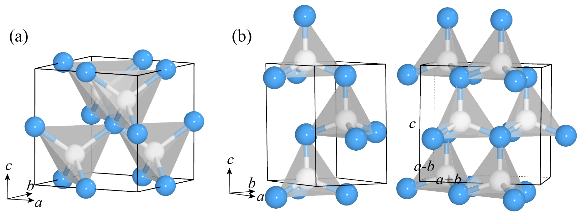
Fig. S1(a) presents the conventional unit cell of cubic phase for both the group-IV elementary substance and group III-V compounds. In the cubic cell, the lattice constants are equal, with , and the angles between the lattice vectors are all 90 degrees, denoted as . The cubic phase of both the III-V group and the IV group materials share the same structure but with different types of atoms. In the case of group-IV systems, the cubic unit cell has a diamond structure and crystallizes in the cubic space group. On the other hand, for group III-V systems, the cubic unit cell adopts a zincblende structure and crystallizes in the cubic space group. In these compounds, there are two types of elements. Each atom in the group-III/V is bonded to four equivalent atoms, forming corner-sharing / tetrahedra. Figure S1(b) illustrates both the primitive unit cell and the orthorhombic supercell of the hexagonal phase in group III-V compounds. The hexagonal phase has a wurtzite structure and crystallizes in the hexagonal space group. The lattice constants for the hexagonal primitive unit cell are , with the angles and . As depicted in Fig. S1(b), the orthorhombic supercell is constructed using the lattice vectors , , and , where , , and are the lattice vectors of the primitive unit cell. Similar to the cubic phase structures, in the hexagonal phase, each atom in group-III/V is also bonded to four atoms to form corner-sharing / tetrahedra with very small deviations to the for bond length compared to the cubic phase.
.2 Mean absolute errors for testing IV and III-V group materials.
Table S1 displays the mean absolute errors (MAE) for evaluating the generalization capability of DeePTB using both group-IV and III-V systems. The notations in the table represent the training data types: cubic () and mixed (), and the testing data types: cubic () and hexagonal ().
| Systems | MAE | ||
|---|---|---|---|
| C | 0.048 | - | - |
| Si | 0.031 | - | - |
| Ge | 0.044 | - | - |
| Sn | 0.045 | - | - |
| AlN | 0.020 | 0.021 | 0.031 |
| AlP | 0.026 | 0.028 | 0.028 |
| AlAs | 0.033 | 0.037 | 0.054 |
| AlSb | 0.029 | 0.036 | 0.037 |
| GaN | 0.022 | 0.024 | 0.048 |
| GaP | 0.016 | 0.019 | 0.036 |
| GaAs | 0.029 | 0.022 | 0.030 |
| GaSb | 0.027 | 0.031 | 0.046 |
| InN | 0.021 | 0.022 | 0.038 |
| InP | 0.027 | 0.028 | 0.053 |
| InAs | 0.028 | 0.032 | 0.039 |
| InSb | 0.027 | 0.024 | 0.028 |
.3 Distributions of bond lengths from training and testing data sets
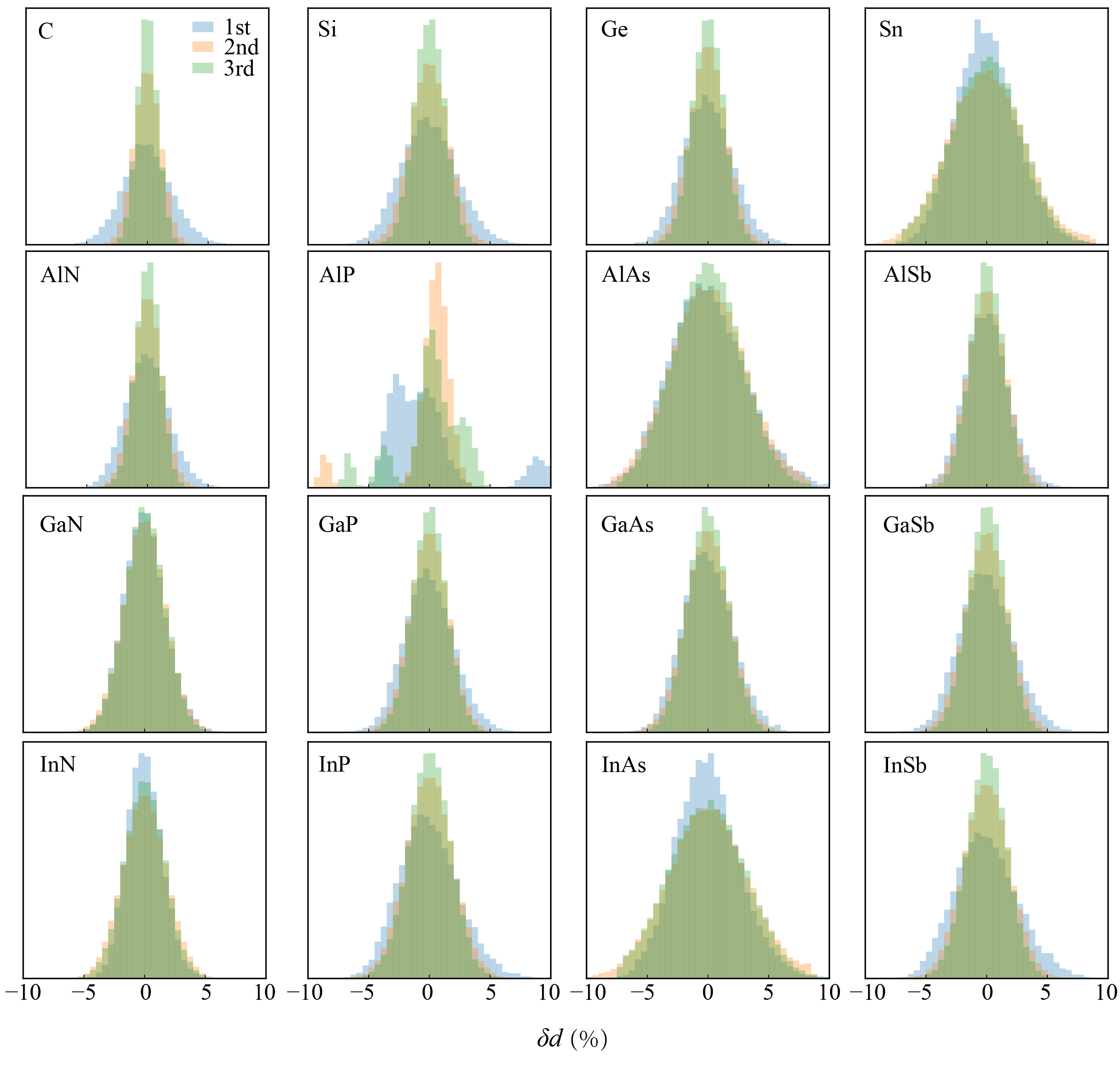
Here, we present the statistical distributions of bond lengths, which represent the separations between pairs of atoms, including up to the 3rd nearest neighbors in the training and testing data sets, which consist of the sampled configurations of MD trajectories. To obtain these distributions, we compute the separations of pair atoms in each configuration individually and then sort them based on their magnitude. We classify the bond lengths based on their magnitude and the types of pair atoms involved. For example, in the case of GaP, the 1st and 3rd bonds correspond to Ga-P bonds, while the 2nd bond corresponds to Ga-Ga and P-P bonds. The variation ratio is calculated by dividing the instantaneous bond length by its equilibrium value. The resulting bond variations for each nearest neighbor are then plotted as distribution density, as shown in Fig. S2. From the figure, we observe that the percentage change in bond lengths is relatively consistent for all the bonds within the same trajectory. Most variations in the materials fall within the range of , generating suitably distorted structures for training and testing our DeePTB model.
.4 Reproduction of ab initio band structures
In the main text, we have demonstrated the ability of the converged DeePTB model to accurately predict the ab initio eigenvalues for unseen structures. To further validate the performance of DeePTB, we compare the predicted band structures with the ab initio counterparts for the undistorted structures with primitive unit cells in all the systems discussed in the main text. The comparison of band structures is presented in Fig.S3 and Fig.S4.
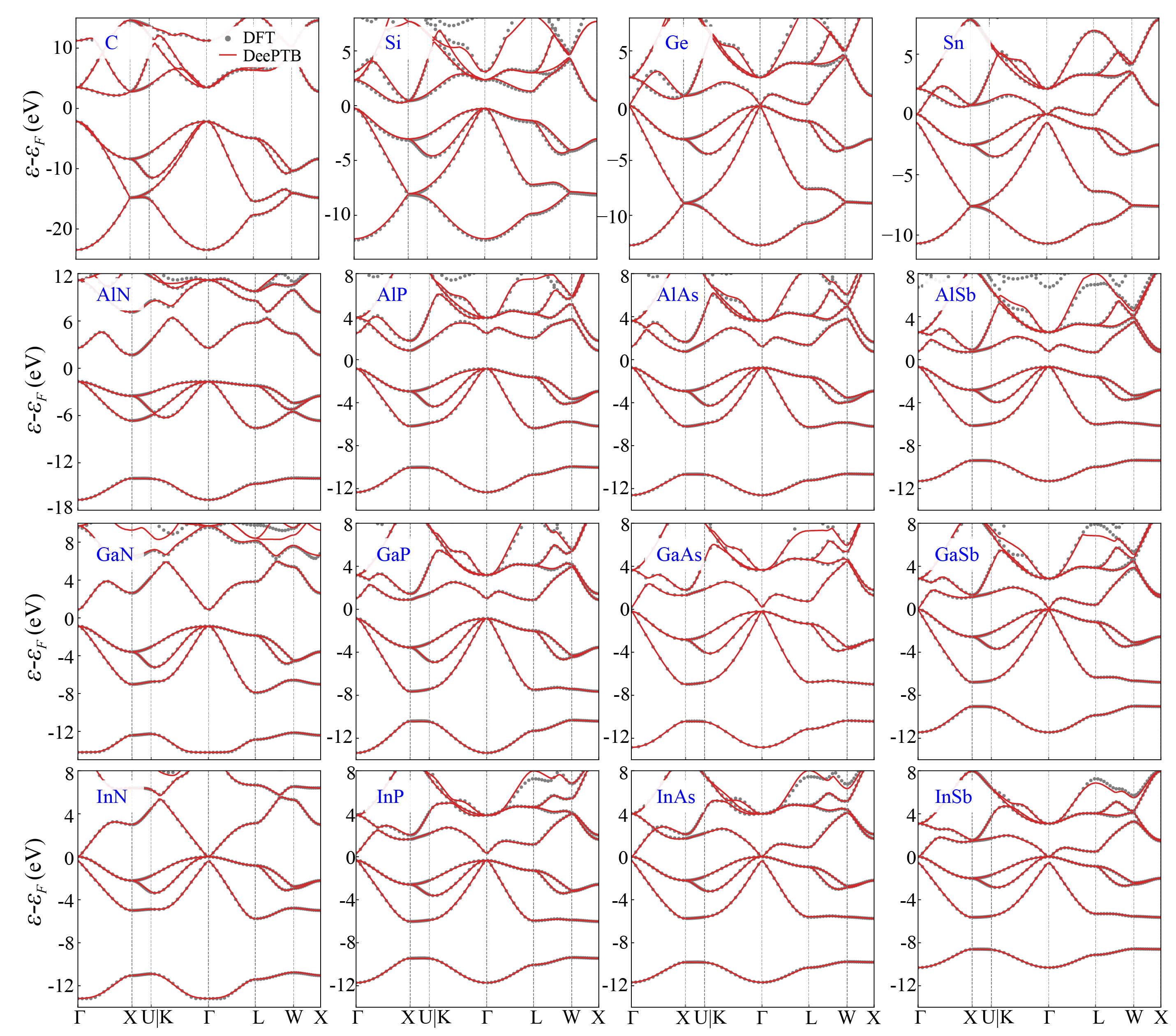
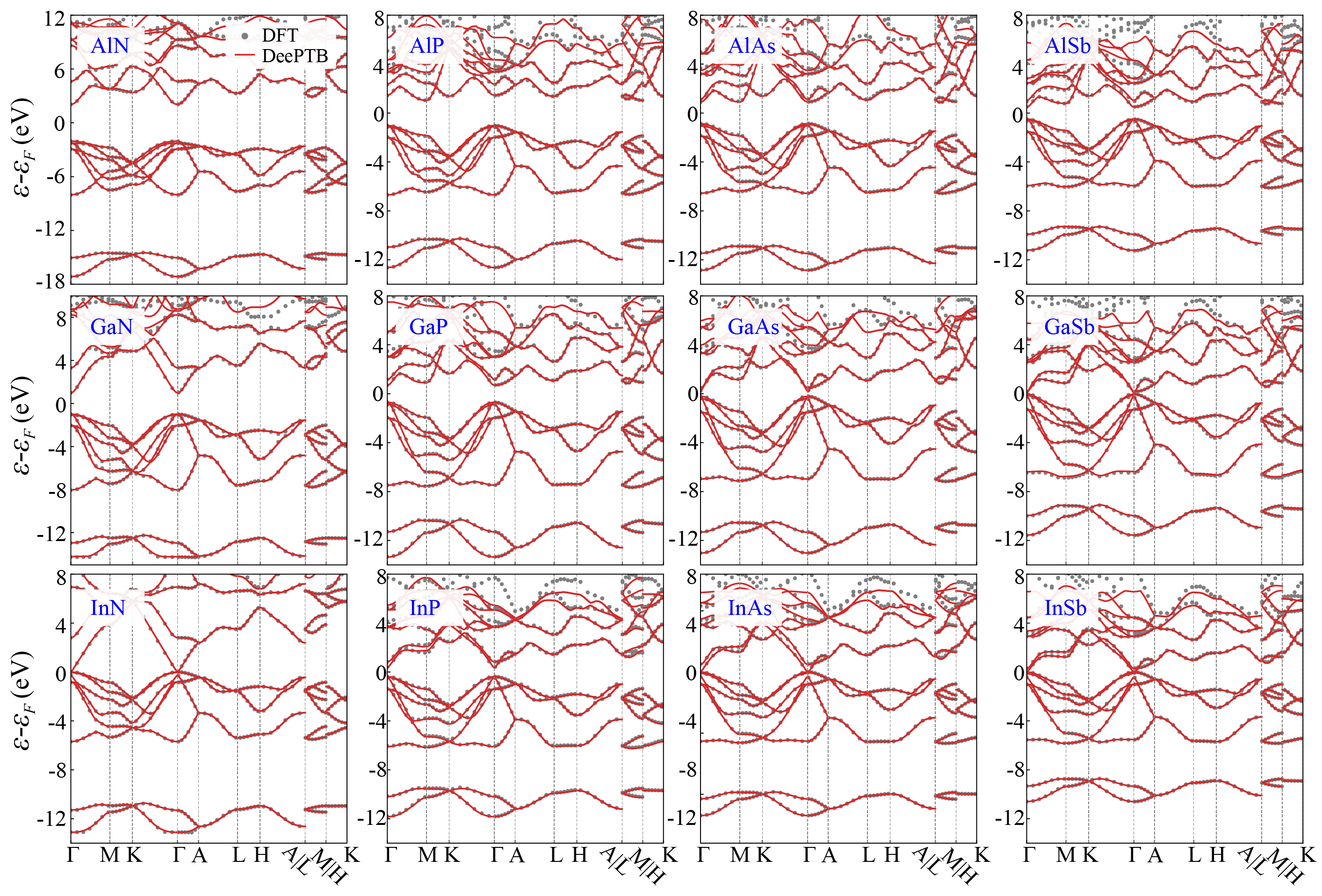
For the cubic phase, the primitive unit cell consists of only two atoms, with a total of 8 valence electrons. In the case of group IV elements, both atoms have an atomic configuration of . On the other hand, for III-V group compounds, the atomic configurations are for group-III elements and for group-V elements, where and are the principal quantum numbers. As a result, there are a total of 4 valence bands, taking into account the spin degeneracy. In our DeePTB model, we consider these 4 valence bands together with the lowest 3 conduction bands as the training labels. To accomplish this, we set a fitting energy window [,], which includes the valence bands and low-energy conduction bands as part of the training labels. We claim that this energy window is independent of the supercell size. After training, the DeePTB model successfully reproduces the band structures, as depicted in Fig. S3, for both group IV and III-V systems. Despite sharing the same lattice structure, the band structures of group IV and III-V systems exhibit notable differences, which are well captured by our DeePTB models. As observed in the results, the DeePTB predictions accurately match the ab initio eigenvalues. For the hexagonal phase of III-V group systems, the primitive unit cell consists of 4 atoms, with 2 atoms belonging to group III and 2 atoms belonging to group V, resulting in a total of 16 valence electrons. As a result, there are 8 valence bands, taking into account spin degeneracy. In our DeePTB model, these 8 valence bands, along with the lowest 4 conduction bands, are utilized as training labels. As depicted in Fig. S4, it is evident that DeePTB accurately reproduces all the considered valence and conduction bands for all the systems.
.5 Flexibility to a different basis, functional and SOC cases
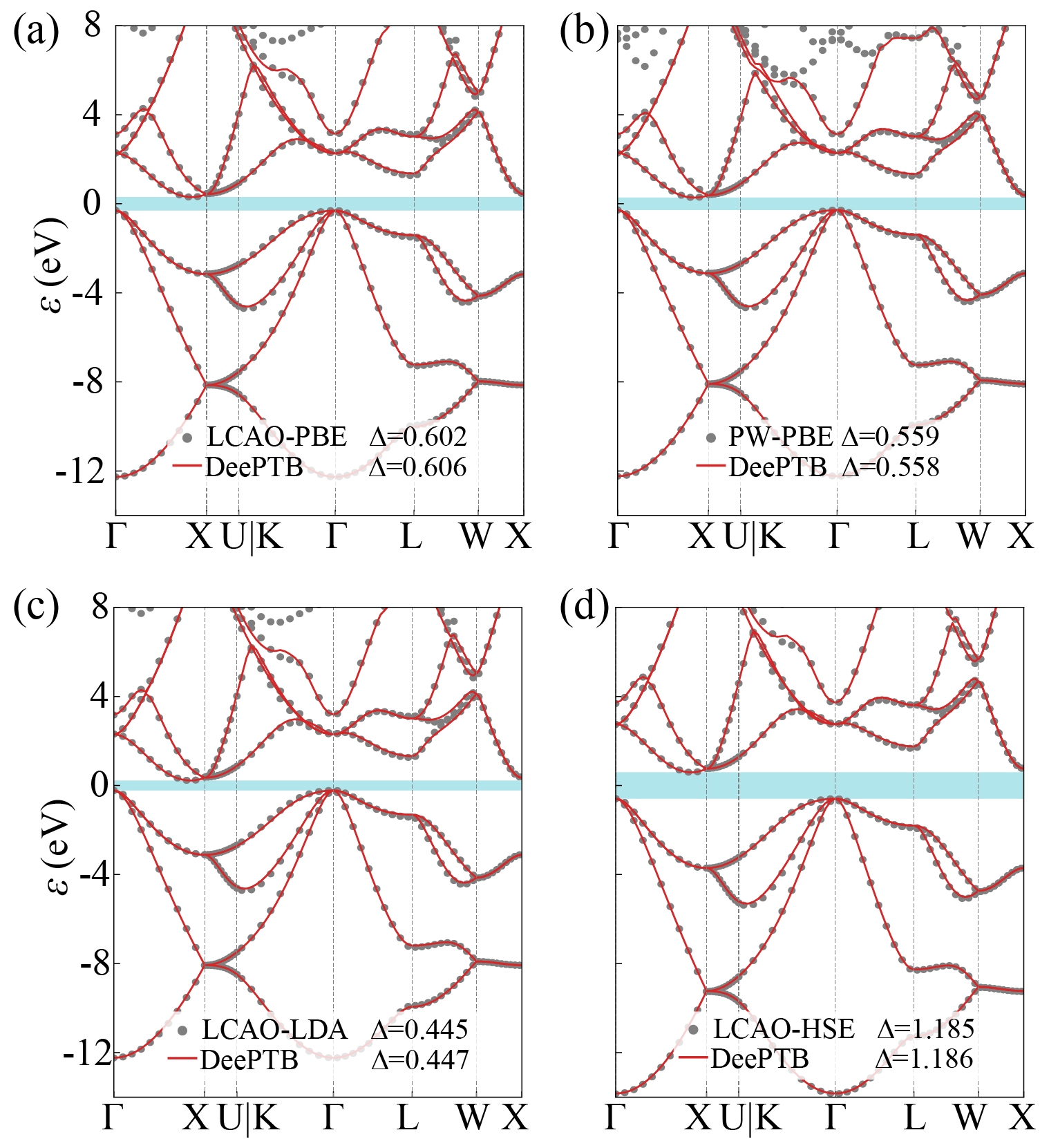
Besides the GaAs example discussed in the main text, we also utilize Si as an additional example to demonstrate the versatility of DeePTB in handling different basis sets and XC functionals. Additionally, we showcase the capability of DeePTB to incorporate the SOC effect in band structures by considering two more examples: InSb and Sn. Figure S5 presents the DeePTB representation of ab initio band structures calculated using various basis sets (LCAO and PW) bases) and XC functionals (LDA, PBE, and HSE). For the LCAO basis, DZP orbitals are employed, while a 100 Ry energy cutoff is utilized for the PW basis The orbitals and 3rd nearest neighbors for both bonds and local environments are utilized in DeePTB, as mentioned previously. To analyze the impact of different basis sets and XC functionals on the band structures of Si, we compare various cases. In Fig.S5(a) and (b), we present the band structures of Si obtained using different basis sets but with the same PBE functional. On the other hand, Fig.S5(a), (c), and (d) depict the results obtained using different XC functionals within the same LCAO basis. While the dispersion of the valence bands and low-energy conduction bands exhibits similarities across these different cases, the band gaps vary significantly. In particular, the ab initio calculations yield a band gap of 0.602 eV and 0.445 eV for the PBE and LDA functionals in the LCAO basis, respectively. However, the HSE functional provides a more accurate band gap of 1.185 eV, which is in closer agreement with the experimental value of 1.17 eV.
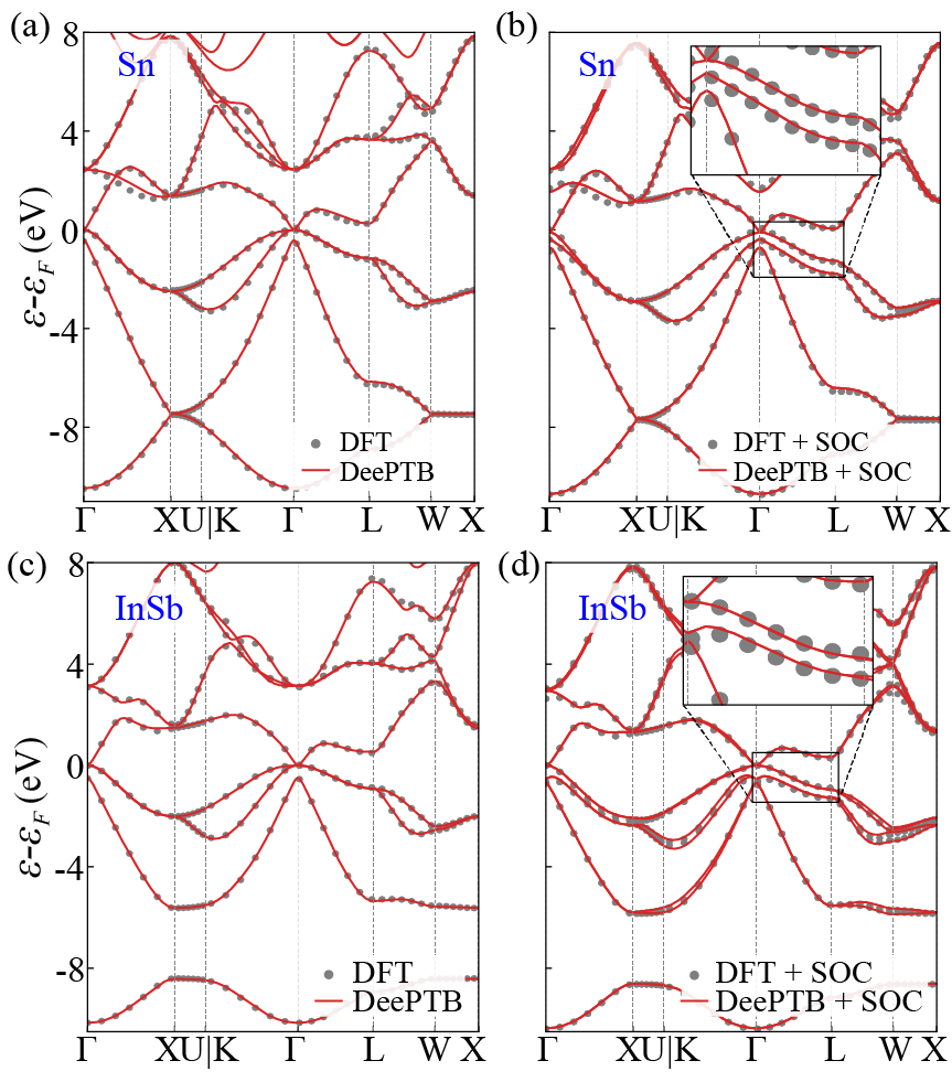
The band structures of InSb and Sn, considering the SOC effect, are displayed in Fig.S6. In these examples, the DeePTB band structures of InSb and Sn exhibit good agreement with the DFT-calculated results, both with and without considering the SOC effect. The presence of SOC leads to the splitting of some degenerate bands observed in the non-SOC band structures, as illustrated in Fig.S6(b) and (d), respectively. The energy splitting is particularly noticeable along the path, with a magnitude of approximately 0.5 eV (Sn) and 0.4 eV (InSb) at the point for both systems. These splitting patterns are accurately captured by DeePTB. The inset of Fig. S6(b) and (d) provides a blow-up view of the two split bands along the path.
The accurate reproduction of the band structures in the above results provides additional evidence that the DeePTB approach is advantageous in its independence from the choices of XC functionals and basis sets, while accurately capturing the effect of SOC. This flexibility of the DeePTB model enables its application in various scenarios that previously required ab initio simulations at different levels of accuracy.