Modelling the response of a CsI(Tl)-PiN photodiode Microscintillator Detector
Abstract
The full instrument response of a superminiaturised CsI(Tl)-PiN photodiode radioactivity detector, intended for deployment on a meteorological radiosonde, has been modelled by combining a physics-based model of the sensor with the detector circuit response, obtained via an LTspice simulation. The model uses the incident energy of a gamma ray as an input, and produces the pulse expected from the detector. The detector response was verified by comparing the simulated energy calibration with a laboratory source. The measurement circuit is found to control the minimum detectable energy of 26 keV, and the maximum detectable energy is 10 MeV. The energy sensitivity of the PiN detector is 0.29 0.02 mV/keV in the 0-800 keV range. The simulation and laboratory calibrations were consistent to better than 5% over the calibration range of the instrument.
keywords:
Radioactivity Detector , Ionisation , Scintillator , PiN Photodiode , Simulation , LTspice[1]organization=Faculty of Engineering, University of Bristol,addressline=Queen’s Building, University Walk, city=Bristol, postcode=BS8 1TR, country=United Kingdom
1 Introduction
There is a lack of readily available instrumentation to study ionisation in the atmosphere, and the effects of energetic particles on weather and climate [1]. The creation of atmospheric ions by galactic cosmic rays, solar UV radiation, and electron precipitation events means that the effects of these ions manifest in different regions of the atmosphere. For instance, neutron monitoring stations provide a global understanding of galactic cosmic ray intensities, however at altitudes below 5 km, it has been shown that there is little correlation between neutron counts and measured ionisation rates [2]. Predominantly, satellites have been used for primary particle detection [3], and ground-based instruments for secondary particle detection, however the intermediary region creates an opportunity for a new, balloon-borne detector.
A novel microscintillator ionisation detector, here called the PiN detector, capable of measuring energy and count rate, has been developed for deployment on meteorological radiosondes (weather balloons). Hundreds of these balloons are launched daily for weather forecasting purposes, but as they are not routinely retrieved, and have limited capability to carry additional payloads, the cost is limited to a few hundred pounds and the mass to tens of grams. Geigersondes are suitable for balloon applications but do not offer energy detection [2]. A miniaturised CsI(Tl) scintillator coupled to a PiN diode both meets the radiosonde power and mass requirements, and adds energy detection capability. The detector was first deployed on a meteorological radiosonde in 2016 to investigate the transition region where surface-borne energetic particles cease to be the dominant source of ionising radiation, in favour of high-energy particles in the free troposphere [4]. During balloon deployment in 2018, the detector unexpectedly observed stratospheric X-rays, which was corroborated by NOAA POES spacecraft data [5]. Deployment of the detector is well-established, however the work presented in this paper analyses and discusses the instrumentation in more detail than previously. This will allow both for retrospective analysis of previous flight data and for future development.
The PiN detector sensor is an Advatech CsI(Tl) scintillator, measuring 10108 mm3, coupled to a silicon PiN RD100 photodiode [6, 7]. There are two stages in particle detection within the sensor. First, incident radiation generates a light pulse in the scintillator, described by characteristic decay times. The second stage of particle detection involves the conversion of a light pulse to a current pulse. The magnitude of the current pulse is proportional to the energy of the incident ionising radiation. The next stage of particle detection involves the current passing through the electronics of the detector. Figure 1 shows the detection process where the current flows from the PiN photodiode to a transimpedance amplifier, located physically close to the photodiode on the board to minimise losses. The signal then passes through a frequency dependent gain stage, followed by the signal conditioning circuitry.
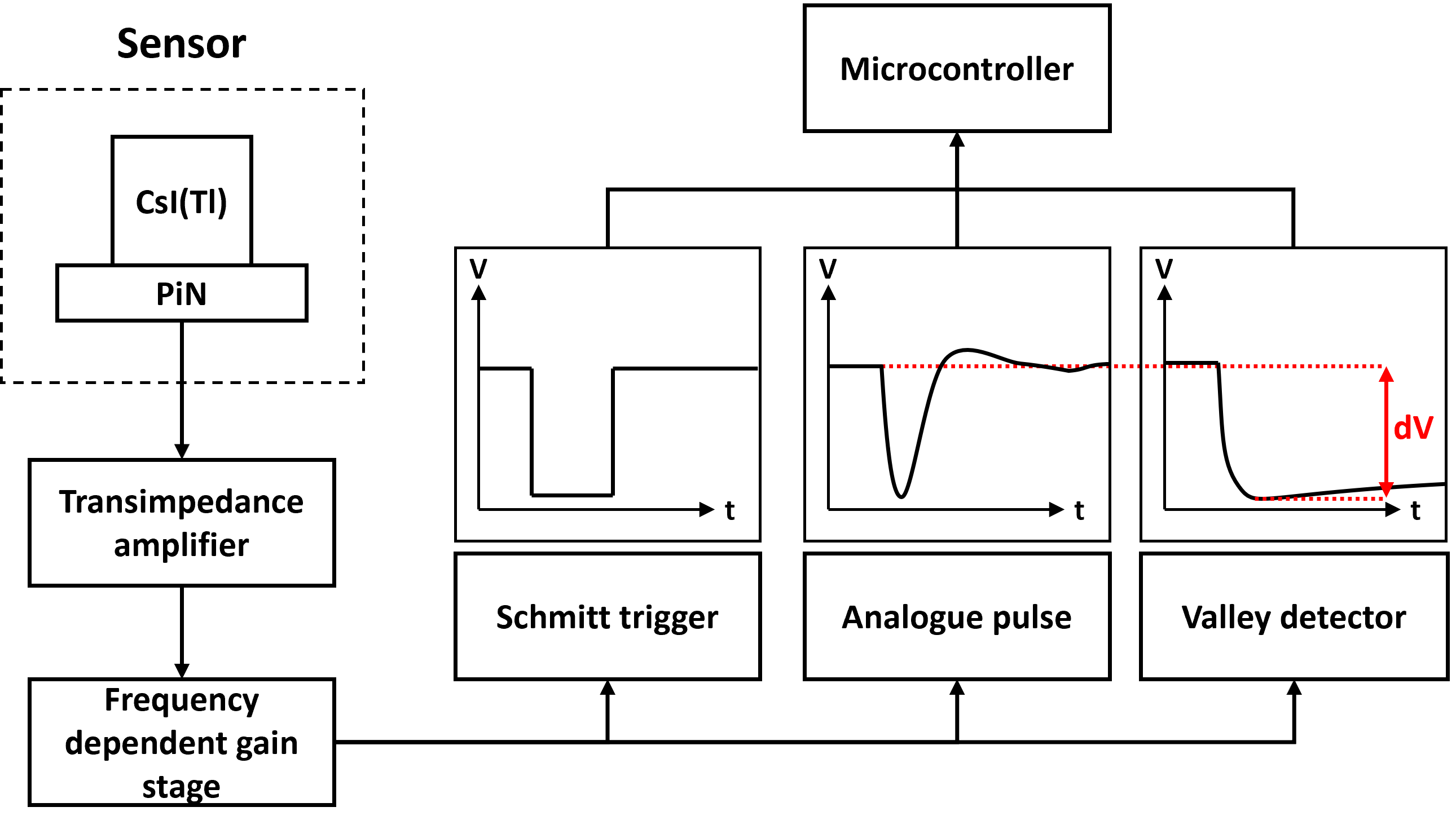
There are three key components in the signal conditioning circuit: a Schmitt trigger, an analogue pulse, and a negative peak detection circuit (valley detector). The trigger activates an interrupt routine in the PIC16F676 microcontroller code, signalling the microcontroller to measure the voltages on the analogue pulse and the valley signal.
A pulse height, , is calculated by the difference between a reference point on the analogue pulse and the valley trace. The measured analogue pulse value is larger than the measured valley value, as the analogue pulse is a negative pulse.
Regarding the detector data collection, the microcontroller has a 10-bit analogue-digital converter (ADC), which with a 5 V supply, gives 5 V as 1023 ADC counts (referred to in the following text as ‘ADC’). The reference voltage level rests at 3.211 V (657 ADC). The pulse height should then not exceed 657 ADC. The microcontroller samples the reference and valley voltage values separately, timestamps them, and sends them to a serial output.
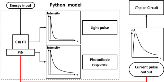
We present, for the first time, a full-stack model of the detector response, from the initial interaction of the scintillator with ionising radiation, through to the production of signals which are passed to the microcontroller for measurement. A physics-based model written in Python emulates the response of the sensor, the signals from which are used as input to a Simulation Program with Integrated Circuit Emphasis (SPICE) simulation to emulate the electronics response of the detector. The model therefore takes a single input energy and produces the corresponding pulse from the detector electronics - modelling the monoenergetic response.
Software packages such as Geant4, FLUKA, and MCNPX are often used to simulate the interactions between ionising radiation and scintillator crystals [8]. FLUKA was not suitable as the desired light pulse output needed to be in the time-domain, to combine with the photodiode response; whereas FLUKA produces quantities such as spatial energy depositions, emission spectra, and particle fluence, among others. Using Geant4 in combination with SPICE programs has been suggested as a method of investigating the overall response of a detector and would likely be a valid approach [9]. However, as the scintillator is a commercial product with its typical response provided by the manufacturer, it would be unnecessary to model its response from first principles. Additionally, as the goal is simulation of the total response of the detector, the response of electronic components used in the signal conditioning circuit are as important as the detailed physics of the sensor itself. This motivates an analytical approach to the model, rather than focusing on the small differences likely to arise between a numerical and analytical approach [10].
Like the scintillator, the photodiode is governed by characteristic decay times (rise- and fall-times); however, as a commercial component, only typical rise times, at a specific reverse bias and for a given wavelength, are provided. Therefore, the rise time has been determined by using estimated parameters, and the fall time was determined during a tuning phase of the model development. Convolution has been used as the method of interfacing the scintillator and photodiode responses [9], ultimately producing a current pulse. Figure 2 illustrates the detection process, noting the output from each stage of the Python model. Finally, the SPICE simulation has been created using LTspice; the current pulse from the physics model is used as an input for the simulation. Relevant circuit components have been recreated in LTspice, allowing for analogue voltage traces to be measured.
Accompanying the model and simulation, a laboratory calibration with a radioactive source is presented, serving as the primary method of validation for the model. Section 2 details the model method, with the scintillator response in Section 2.1, the photodiode response in Section 2.2, and the current pulse in Section 2.3. Simulation of the detector electronics is detailed in Section 2.4, and the laboratory calibration is explored in Section 3. Finally, a comparison of the model and detector is given in Section 4.
2 Model Method
Modelling the PiN detector response was split into two sections: the physics model, and the electronics simulation. Within the physics model, the responses of the scintillator and photodiode are considered, resulting in their combination which produces a current pulse proportional to the incident radiation. The current pulse serves as an input for the electronics simulation. The simulation models the remainder of the detector until the data acquisition stage.
2.1 CsI(Tl) Scintillator Response
To model the production of photons by the interaction of radiation with the scintillator, the following assumptions were made [11, 12]:
-
1.
Total number of photons generated are determined by the light yield - the number of photons emitted per unit energy () - of the scintillator
-
2.
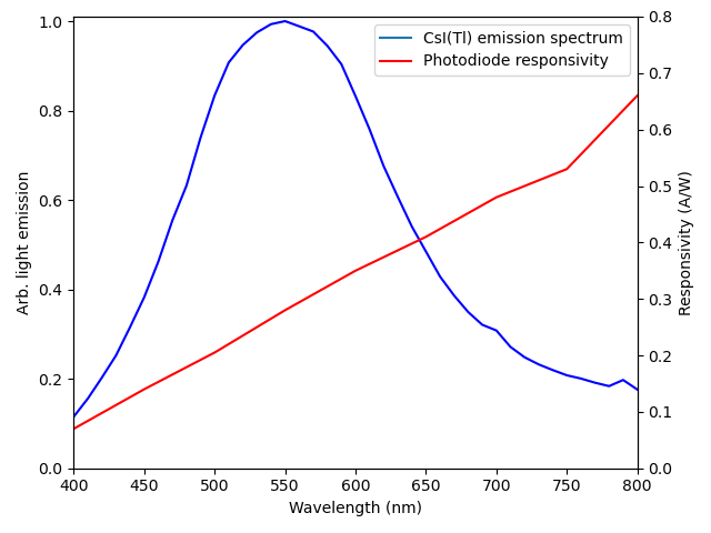
Photons are emitted over a range of wavelengths in different proportions, described by the emission spectrum
-
3.
The light pulse generated is characterised by at least two decay times
The scintillator emission decay curve is described by Equation 1
| (1) |
where is scintillator rise time, are the fast and slow decay times, respectively, and their proportions. If additional decay components are desired, they can be added to Equation 1, with the limit that the summation of proportions is equal to one. In the instance of the CsI(Tl) crystal present in the PiN detector, the manufacturer reports a single decay time, therefore in the model . The scintillator parameters are given in Table 1, and different numbers of decay components are considered in Section 4.3.
The model uses discretised wavelength steps to determine the energy generated by scintillation photons during an interaction. For each wavelength, , a number of photons, are produced described by the light yield , incident energy , and emission spectrum proportion :
| (2) |
The emission spectrum, shown in Figure 3, was digitised using a Python-based plot digitiser and linear interpolation [13, 14]. This processes allows for the scintillator emission spectrum and the photodiode responsivity to be evaluated at the same steps (every 10 nm) over the model’s wavelength range (400-800 nm). Therefore, a summation of the energy of a single wavelength photon, , multiplied by the corresponding number of photons, over this range, yields the total energy emitted by the scintillator for a single event.
| (3) |
It is necessary to convert the energy emitted from the scintillator into a power quantity, because the photodiode responsivity relates incident optical power to an output photocurrent - discussed in Section 2.3. Therefore, an energy dependent function (cutoff time), , has been empirically determined.
| (4) |
The cutoff time function returns a single value in s. The function was determined by evaluating test values until a small (2 %) percentage difference was present between the model output and the expected output (determined by the laboratory calibration).
The final expression for the power output from the scintillator is then
| (5) |
| Parameter | Symbol | Value | Source |
|---|---|---|---|
| Scintillator rise time | 50 ns | Estimated [15] | |
| Fast decay time | 900 ns | Datasheet [6] | |
| Slow decay time | N/A | N/A | |
| Cutoff time | - Variable | Empirical function | |
| Fast decay proportion | 1 | Datasheet [6] | |
| Slow decay proportion | 0 | N/A | |
| Light yield | LY | 54000 /MeV | Datasheet [6] |
2.2 PiN Photodiode Response
The temporal response of the photodiode is governed by the rise time , typically composed of: drift and diffusion times, and the RC time constant of the diode circuit. The relationship between the three components is given by:
| (6) |
where , , and are the RC, drift times, and diffusion times, given in Equation 7, 11, and 12 respectively.
The derivation of the RC time constant and its dependencies are given in Equations 7-10 which denote the RC time constant, the junction capacitance , the depletion width , and the series resistance [16]:
| (7) |
where is the load resistance which has been estimated;
| (8) |
where is the relative permittivity of silicon, is the permittivity of free space, and mm2 is the active area of the photodiode;
| (9) |
where is the charge of an electron, V is the applied bias, V is estimated value of the built-in bias of silicon (which has typical forward bias between 0.6-0.7 V), and is the doping concentration;
| (10) |
where is the resistivity of silicon and is the electron mobility, =0 is the assumed contact resistance in the diode, and is the silicon substrate width.
The substrate width and doping concentration were estimated by considering the case where V, and the photodiode is completely depleted, meaning . Using the previous assumption, Equation 8 and the typical value of the junction capacitance, 50 pF, under such conditions, the substrate width is estimated to be m. Following, an estimate for the doping concentration can be obtained using this result and Equation 9, giving .
Additionally, the electron mobility of silicon =1350 cm2(Vs)-1 [17].
The drift time [16] component is given by:
| (11) |
The diffusion time [16] is given by:
| (12) |
where is the hole mobility equal to 480 cm2(Vs)-1 [17].
A summary of the photodiode model parameters are given in Table 2.
The PiN photodiode response curve is given by
| (13) |
where the photodiode fall-time .
The rise time governs the rate at which the photodiode can respond to a pulse of light. Typical literature values for the rise time are reported for the case where the photodiode is operated in its fully depleted mode at a reverse bias of 75 V. It was therefore necessary to obtain a rise time for the conditions employed in practice. This was completed by setting the reverse bias to 12 V and using Equations 6-12 with the above calculated and . A rise time of 15.08 s was obtained as a result. The photodiode fall time was determined by matching the ADC pulse height for the 137Cs 662 keV energy peak in the simulation and the calibration and remained fixed at this value. This parameter, ultimately, serves as a “catch-all” for inaccuracies which might arise in the estimation of the doping concentration of silicon, or the substrate width. Therefore, while model parameters have been chosen in Table 2, there are other possible combinations which yield the same rise time.
| Parameter | Symbol | Value | Source |
|---|---|---|---|
| Silicon doping concentration | 2.985 1018 | Estimated from [7] | |
| Substrate width | 210.7252 m | Estimated from [7] | |
| Load resistance | 50 | Estimated [7] | |
| Contact resistance | 0 | Assumed | |
| Electron mobility | 1350 | Estimated [17] | |
| Hole mobility | 480 | Estimated [17] | |
| Silicon built-in bias | 0.65 V | Estimated | |
| Photodiode rise time | 15.08 s | Derived | |
| Photodiode fall time | 32 s | Empirical |
2.3 Current Pulse
The current pulse is given by a convolution of the scintillator and photodiode response, using the photodiode responsivity - digitised and shown in Figure 3 - to convert from the scintillator power to electrical current [18]. The current pulse, is given by:
| (14) |
where is the photodiode responsivity over the same wavelength range as the scintillator emission spectrum. The responsivity is the ratio of current generated to optical power. The magnitude of the current pulse is given explicitly by:
| (15) |
Where, , denotes the maximum value of the convolution therefore serving as a normalisation factor.
2.4 Electronics Simulation
The current pulse from the physics model has been used as a current source input in LTspice. The current source is connected to the transimpedence amplifier, yielding a voltage trace. The remainder of the circuit - until the microcontroller - was built in LTspice, following the layout given in Figure 1. The measurement of the pulse analogue and valley detector voltages were completed manually, converting the voltage into an analogue-to-digital count. By varying the input energy, a relationship between incident energy and pulse height was determined.
3 Laboratory Calibration
To validate the model, a PiN detector was calibrated using a Cesium-137 (137Cs) radioactive source, and a P-2000 NaI(Tl) spectrometer. The P-2000 uses a 3.8 cm diameter by 2.5 cm thick NaI(Tl) crystal coupled to a photomultiplier tube (PMT) with diameter of 5.1 cm. The PMT is connected to a 1 kV multi-channel analyser, with data recorded via the Genie2000 software. The probe reports a resolution of 8.5 %. The experimental setup for the 137Cs source can be seen in Figure 4(a). During 137Cs data collection, both instruments were aligned as seen in Figure 4(b). The activity of the 137Cs source was Bq and both instruments were placed 45 1 cm from the source. The PiN detector was exposed to the source for 287.96 seconds, and the spectrometer was exposed for 421 seconds.
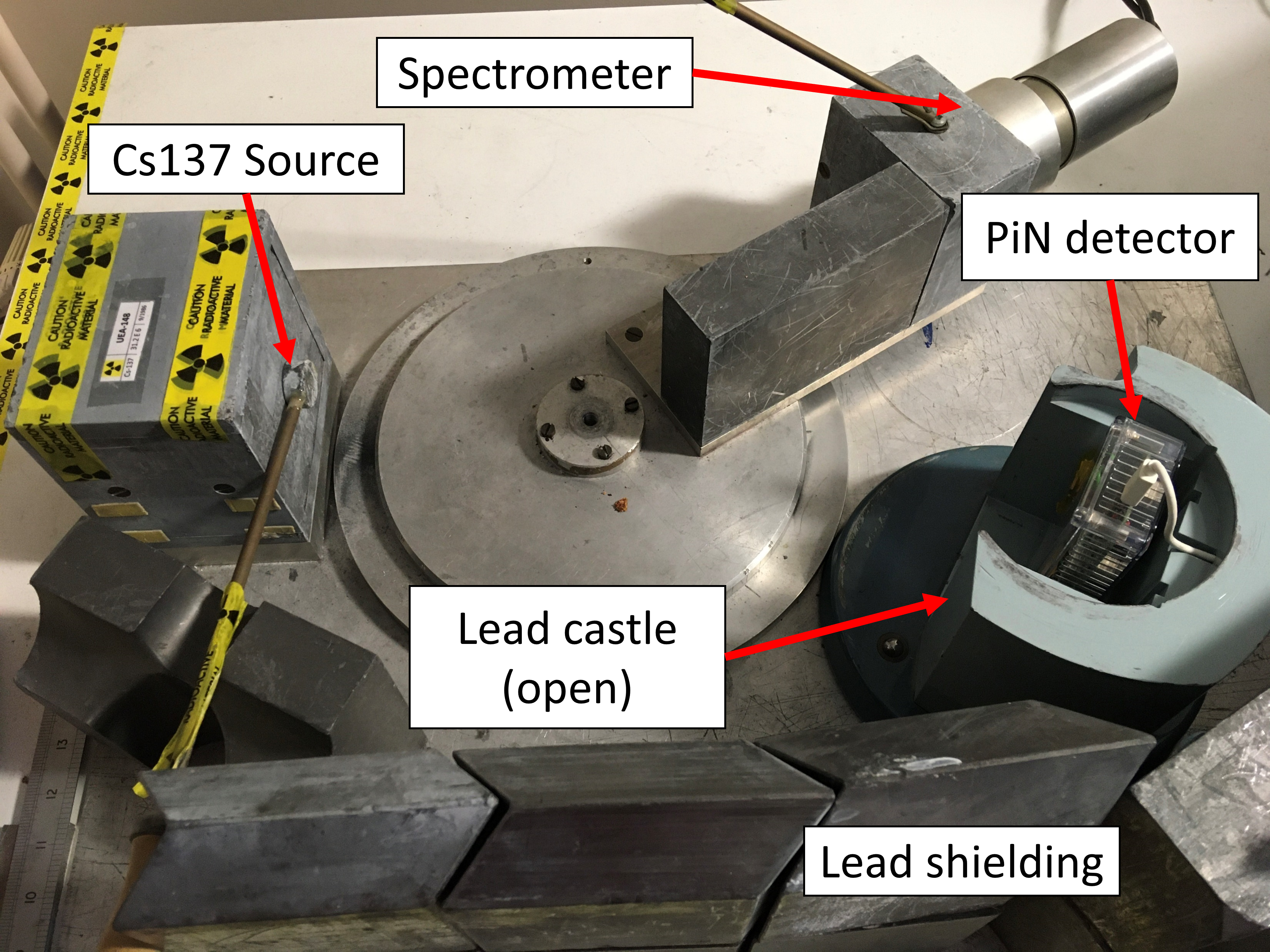

Figure 5 displays the raw binned PiN data from the 137Cs source, the processed spectrum, and the count rate from the data set. To obtain the processed spectrum, the error on a single pulse height (1 ADC) is considered. From the list of pulse heights, a new list is created where each event is 1 ADC greater than its original value and another list where each event is 1 ADC smaller. These two lists and the original list are binned normally, and the frequency in each bin is averaged.

3.1 PiN Detector and P-2000 Spectrometer
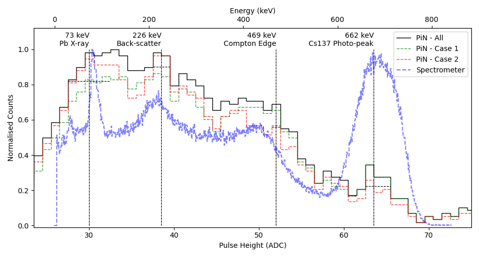
The P-2000 spectrometer allows for energy peaks in the PiN detector spectrum to be identified. The spectrometer was first calibrated using the energy peaks detailed in Table 3 (R2 = 0.9909, p-value 0.0004); the errors on P-2000 energy values were given by the spectrometer calibration. Figure 6 overlays the energy and pulse height spectra from each instrument. The two spectra were aligned by adjusting the pulse height limits in the PiN spectrum until its shape matched that of the NaI(Tl) spectrum. The location of the features seen in the PiN spectrum were then compared to the energy at that location in the spectrometer. In Figure 6, due to the spectrometer calibration, the Compton edge of the spectrometer is at 430 keV; the marked vertical line at 469 keV is the energy at that location in the plot, where an edge can be seen in the PiN spectrum.
| Origin | Characteristic Energy (keV) | P-2000 Energy (keV) |
|---|---|---|
| K- X-ray (137Ba) | 31 | 30 20 |
| Pb X-rays | 88 | 80 30 |
| Back-scatter Peak | 200 | 220 30 |
| Compton Edge | 477 | 430 50 |
| 137Cs Photo-peak | 662 | 680 60 |
Additionally, Figure 6 contains two subsets of data referred to as case 1 and case 2. In the 137Cs data, 60 pairs of events (120/562 events total) occur at the same timestamp, i.e. are simultaneous to less than 100 s. There are several possible reasons: detector error through double-counting, coincidence, or a gamma and beta, which can be emitted simultaneously for some events in small detectors [17]. To deal with this two approaches have been taken to this data: case 1 displays all the ‘unique’ time events and the larger event of each of the 60 pairs (i.e. it ignores the smaller of the ‘simultaneous’ detections). Case 2 displays the unique time events and the smaller of each pair. While beyond the scope of this study, it is interesting to note how well case 2 matches the low energy region of the spectrometer spectrum, suggesting it could be due to the small detector effect of scattered beta particles.
An energy calibration of the PiN detector was completed by linear regression using the energy peaks identified in Figure 6.
The energy calibration, giving the relationship between pulse height ( in ADC) and output energy, is given below where (in keV) is energy determined via linear regression:
| (16) |
with R2 = 0.9997 and p-value 0.0001.
4 Comparison of Detector and Model
4.1 Simulation and Laboratory Results
The laboratory calibration allows for pulses caused by specific gamma energies to be identified. A further verification of the simulation can be obtained by using the gamma peaks identified in the lab as model inputs to predict the detector’s peaks. The relationship between the model input energy (keV) and the pulse height (ADC) is given by:
| (17) |
This linear fit has an R2 = and p-value . Figure 7 shows the selected energy peaks and the pulse heights as measured and predicted. In the 0-800 keV energy range, the percentage difference between measurement and prediction is between 2.00 % and -2.81 %.

The laboratory calibration yields an energy resolution of 17 2 keV/ADC and sensitivity of 0.29 0.03 mV/keV.
4.2 Detectable Energy Range
The smallest detectable pulse height corresponds to the minimum detectable energy. There are several ways to determine this. A physics based approach would be to consider the energies of particles that can pass through the screening can in which the assembly is housed. The enclosure allows through 95 % of 160 keV gamma rays, but 160 keV ( 34 ADC) is much higher than the minimum recorded pulse height, therefore this threshold is not considered to be the limiting factor.
An electronics based approach would be to consider how pulses are measured. When the Schmitt trigger activates (dropping from 5 V to 0 V as shown in Figure 1), a microcontroller interrupt starts the measurement of the valley and reference voltages. For some energies, the Schmitt trigger partially activates, dropping from 5 V to a voltage between 5 and 0 V. For the Schmitt trigger to activate the measurement interrupt, the input pulse must reach the trigger threshold, determined by the circuitry [19]. Therefore, the minimum energy corresponds to the smallest pulse that will fully activate the trigger.
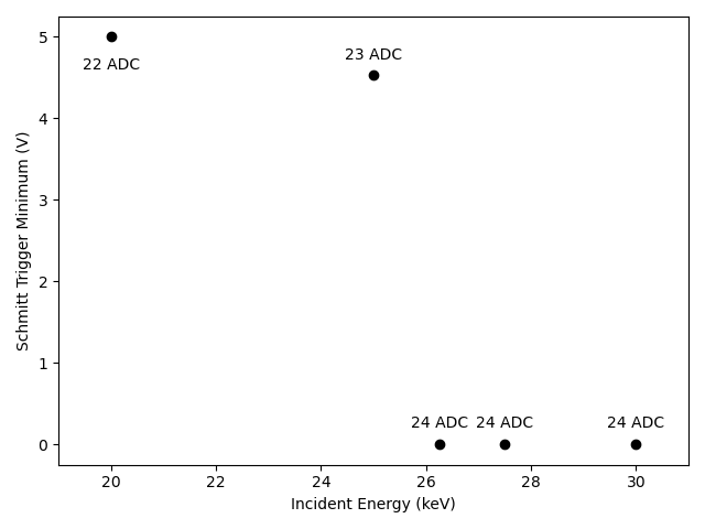
Figure 8 shows the minimum value of the simulated Schmitt trigger for input energies between 20-30 keV. Over this range, the two lowest energies in Figure 8 would not be detected because the Schmitt trigger has not activated. The trigger is set to respond to pulses 20 ADC below the reference level to manage signal-to-noise. If the trigger were made more sensitive it would not be possible to distinguish between electrical noise and very low energy particles.
By using the model described in this paper, it can be seen that pulses corresponding to energy greater than or equal to 26 keV would be detected in the physical system, as there would be full activation of the trigger. Gamma rays with energy in the 24-26 keV range only partially activate the Schmitt trigger and are not detected.
In the 137Cs calibration experiment, the smallest pulse measured was 20 ADC, whereas Figure 8 shows the smallest detectable pulse height in the simulation is 24 ADC. This difference between simulation and measurement is almost certainly caused by fluctuations in the reference voltage, which varies by typically 2 ADC. The detection threshold of 20 ADC corresponds to unphysical negative energies in the calibration experiments, which is most likely due to a lack of high resolution, low energy (100 keV) peaks to optimise the calibration in this region.
The maximum detectable energy could be governed by several aspects. Assuming normal behaviour of the reference level, the maximum pulse height could be 657 ADC, corresponding to an energy of 10-11 MeV, purely considering the available voltage drop. However, more likely the limiting factor on the maximum detectable energy would be the absorption efficiency of the scintillator. For similar sized CsI(Tl) crystals, the absorption efficiency has been shown to decrease to 10% at 10 MeV [20]. The maximum detectable energy is therefore assumed to be 10 MeV.
In summary, the trigger threshold voltage currently determines the minimum detectable energy. The threshold value could be adjusted to increase sensitivity to lower-energy particles, but this would need to be carefully traded off against the level of noise observed in the detector. The maximum detectable energy is controlled by the decrease in sensitivity of the detector at high energies, with the full range approximately 26 keV - 10 MeV.
4.3 Model considerations
Due to the commercial nature of the photodiode used in the detector, a number of the parameters had to estimated. Some combinations of parameters result in the same predicted response. For example, if the scintillator cutoff time is decreased, producing a larger optical power, or the photodiode fall time increased, or the photodiode rise time decreased, all of these increase the size of the final pulse for constant input energy. The photodiode rise time in turn is dependent on the doping concentration, electron and hole mobilities, and resistances in the diode circuit. Therefore, flexibility is available in these model parameters to fine tune its performance to more closely match the actual system.
Additionally, CsI(Tl) crystals are often described by different decay times. We have considered the model sensitivity to three sets of decay parameters. Figure 9 shows the difference between the laboratory calibration, and calibrations obtained from the three sets of additional decay times (B[21], C[11] & D[22]), and the initial Advatech single decay time (A).
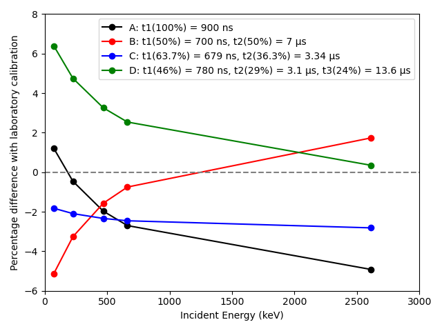
For set C, the absolute percentage difference over this energy range is 1.1 %, suggesting that the scintillator in the PiN detector could be more accurately described by these decay times than a single decay time. However, rather than pick an arbitrary set of decays, the single decay time is retained in the model. Set B spans the largest range of deviation (7 %), however in the mid energy range (500-2000 keV), these parameters lie closest to the laboratory calibration. The large deviation of set D at the low energy range suggests that this model should not be used for scintillator crystals described by similar decay times. Further work could more accurately determine the decay time constants for the scintillator sensor used.
5 Conclusion
A model has been developed to emulate the sensor and electronics response of a miniaturised CsI(Tl) PiN photodiode ionisation detector. The rise and decay times for the scintillator are specified as 50 ns and 900 ns, respectively. The final photodiode rise time was determined to be 15.08 s and fall time was determined to be 35 s. The combination of a physics model and an electronics simulation have resulted in a full detector model which has been verified against a laboratory calibration with a 137Cs source. At 100 keV the difference between the model and laboratory data was 0.64 %, and at 800 keV, it was -2.81 %. This modelling plus new calibration techniques have led to improvements in the detector energy resolution compared to previous work [4][5], to typically 17 1 keV, in a range of 100 - 800 keV. This is suitable for the intended meteorological radiosonde application, as data rate limitations typically further degrade the energy resolution.
The model has been used to suggest that the Schmitt trigger threshold voltage appears to determine the minimum detectable energy of approximately 26 keV. Agreement between the predicted and measured response means that components in the electronics can confidently be changed and tested in the simulation before implementation, speeding up development. Despite the PiN photodiode being a commercial product, with some physical quantities kept as proprietary information, the model affords flexibility in choosing, and matching, the photodiode fall time to accommodate parameters which have otherwise been estimated or assumptions which may not hold. It can also be adapted to simulate changes in the system such as different scintillator material or the response at different temperatures.
Overall this investigation offers increased confidence in the response of the detector, especially when considering the minimum detectable energy. This aspect is particularly valuable when evaluating the atmospheric effects of bremstrahhlung X-rays from energetic electron precipitation during space weather events [5]. Overall the model and laboratory calibration were consistent to an absolute difference better than 5% over the calibration range (0-800 keV) of the instrument. The detailed understanding now acquired of this novel miniaturised instrument will allow for more effective analysis and interpretation of existing data and future design improvements.
Data availability
Data is available at Tabbett, Justin; Aplin, Karen (2023), “PiN Modelling Data”, Mendeley Data, V1, doi: 10.17632/mctr9ksk4r.1
Acknowledgements
We would like to thank Dr Alessandro Narduzzo at the Department of Physics, University of Bath for access to radioactive sources.
Funding
EPSRC studentship and A-Squared Technologies Ltd.
References
- Mironova et al. [2015] I. A. Mironova, K. L. Aplin, F. Arnold, G. A. Bazilevskaya, R. G. Harrison, A. A. Krivolutsky, K. A. Nicoll, E. V. Rozanov, E. Turunen, I. G. Usoskin, Energetic Particle Influence on the Earth’s Atmosphere, Space Science Reviews 194 (2015) 1–96. URL: https://doi.org/10.1007/s11214-015-0185-4. doi:10.1007/s11214-015-0185-4.
- Harrison et al. [2014] R. G. Harrison, K. A. Nicoll, K. L. Aplin, Vertical profile measurements of lower troposphere ionisation, Journal of Atmospheric and Solar-Terrestrial Physics 119 (2014) 203–210. URL: https://www.sciencedirect.com/science/article/pii/S1364682614001850. doi:https://doi.org/10.1016/j.jastp.2014.08.006.
- Baumgardner et al. [2011] D. Baumgardner, J. Brenguier, A. Bucholtz, H. Coe, P. DeMott, T. Garrett, J. Gayet, M. Hermann, A. Heymsfield, A. Korolev, M. Krämer, A. Petzold, W. Strapp, P. Pilewskie, J. Taylor, C. Twohy, M. Wendisch, W. Bachalo, P. Chuang, Airborne instruments to measure atmospheric aerosol particles, clouds and radiation: A cook’s tour of mature and emerging technology, Atmospheric Research 102 (2011) 10–29. URL: https://www.sciencedirect.com/science/article/pii/S0169809511002122. doi:https://doi.org/10.1016/j.atmosres.2011.06.021.
- Aplin et al. [2017] K. L. Aplin, A. A. Briggs, R. G. Harrison, G. J. Marlton, Measuring ionizing radiation in the atmosphere with a new balloon-borne detector, Space Weather 15 (2017) 663–672. URL: https://agupubs.onlinelibrary.wiley.com/doi/abs/10.1002/2017SW001610. doi:https://doi.org/10.1002/2017SW001610. arXiv:https://agupubs.onlinelibrary.wiley.com/doi/pdf/10.1002/2017SW001610.
- Aplin et al. [2021] K. L. Aplin, G. J. Marlton, V. Race, Stratospheric X-Rays Detected at Midlatitudes With a Miniaturized Balloon-Borne Microscintillator-PiN Diode System, Space Weather 19 (2021) e2021SW002809. URL: https://agupubs.onlinelibrary.wiley.com/doi/abs/10.1029/2021SW002809. doi:https://doi.org/10.1029/2021SW002809. arXiv:https://agupubs.onlinelibrary.wiley.com/doi/pdf/10.1029/2021SW002809, e2021SW002809 2021SW002809.
- Advatech UK Limited [2023] Advatech UK Limited, CsI(Tl) - Cesium Iodide (Thallium), available at https://www.advatech-uk.co.uk/csi_tl.html, 2023. Accessed on July 21st, 2023.
- OSI Optoelectronics [2023] OSI Optoelectronics, High Breakdown Voltage, Fully Depleted Series [Datasheet], available at https://docs.rs-online.com/558c/0900766b816684f7.pdf, 2023. Accessed on February 10th, 2023.
- Tajik and Ghal-Eh [2015] M. Tajik, N. Ghal-Eh, Comparison of light transport-incorporated mcnpx and fluka codes in generating organic scintillators responses to neutrons and gamma rays, Nuclear Instruments and Methods in Physics Research Section A: Accelerators, Spectrometers, Detectors and Associated Equipment 791 (2015) 65–68. URL: https://www.sciencedirect.com/science/article/pii/S0168900215005318. doi:https://doi.org/10.1016/j.nima.2015.04.043.
- Ogawara and Ishikawa [2016] R. Ogawara, M. Ishikawa, Signal pulse emulation for scintillation detectors using geant4 monte carlo with light tracking simulation, Review of Scientific Instruments 87 (2016) 075114. URL: https://aip.scitation.org/doi/abs/10.1063/1.4959186. doi:10.1063/1.4959186. arXiv:https://aip.scitation.org/doi/pdf/10.1063/1.4959186.
- Pozzi et al. [2007] S. A. Pozzi, M. Flaska, A. Enqvist, I. Pázsit, Monte carlo and analytical models of neutron detection with organic scintillation detectors, Nuclear Instruments and Methods in Physics Research Section A: Accelerators, Spectrometers, Detectors and Associated Equipment 582 (2007) 629–637. URL: https://www.sciencedirect.com/science/article/pii/S0168900207019493. doi:https://doi.org/10.1016/j.nima.2007.08.246.
- Valentine et al. [1993] J. D. Valentine, W. W. Moses, S. E. Derenzo, D. K. Wehe, G. F. Knoll, Temperature dependence of CsI(Tl) gamma-ray excited scintillation characteristics, Nuclear Instruments and Methods in Physics Research Section A: Accelerators, Spectrometers, Detectors and Associated Equipment 325 (1993) 147–157. URL: https://www.sciencedirect.com/science/article/pii/016890029391015F. doi:https://doi.org/10.1016/0168-9002(93)91015-F.
- Hamada et al. [2001] M. Hamada, F. Costa, M. Pereira, S. Kubota, Dependence of scintillation characteristics in the CsI(Tl) crystal on Tl/sup +/ concentrations under electron and alpha particles excitations, IEEE Transactions on Nuclear Science 48 (2001) 1148–1153. doi:10.1109/23.958740.
- Belogurov et al. [2000] S. Belogurov, G. Bressi, G. Carugno, E. Conti, D. Iannuzzi, A. Meneguzzo, CsI(Tl) infrared scintillation light yield and spectrum, Nuclear Instruments and Methods in Physics Research Section A: Accelerators, Spectrometers, Detectors and Associated Equipment 449 (2000) 254–259. URL: https://www.sciencedirect.com/science/article/pii/S0168900299014199. doi:https://doi.org/10.1016/S0168-9002(99)01419-9.
- Singh [2022] D. Singh, Plotdigitizer, https://github.com/dilawar/PlotDigitizer, 2022.
- Xi-Lei et al. [2011] S. Xi-Lei, L. Jun-Guang, H. Tao, Z. Li, C. Jun, W. Yi-Fang, Z. Liang, Y. Bo-Xiang, C. Xiao, F. Jian, X. Yu-Guang, A. Zheng-Hua, W. Zhi-Gang, X. Zhen, Z. Ai-Wu, L. Qi-Wen, N. Fei-Peng, G. Yong-Shuai, L. Ying-Bao, Fast light of CsI(Na) crystals, Chinese Physics C 35 (2011) 1130. URL: https://dx.doi.org/10.1088/1674-1137/35/12/009. doi:10.1088/1674-1137/35/12/009.
- OSI Optoelectronics [2023] OSI Optoelectronics, Application Note 02 - Silicon Photodiodes Physics and Technology, available at https://osioptoelectronics.com/media/pages/knowledgebase/fe8e0c0873-1675100537/an-02-silicon-photodiode-physics-technology.pdf, 2023. Accessed on November 21st, 2023.
- Knoll [1989] G. F. Knoll, Radiation detection and measurement, 2nd ed., Wiley New York, 1989.
- OSI Optoelectronics [2023] OSI Optoelectronics, Photodiode Characteristics and Applications, available at https://www.osioptoelectronics.com/application-notes/an-photodiode-parameters-characteristics.pdf, 2023. Accessed on September 21st, 2022.
- Horowitz and Hill [2015] P. Horowitz, W. Hill, The art of electronics, 3rd ed., Cambridge University Press, New York, NY, USA, 2015.
- First Sensor [2023] First Sensor, First Sensor PIN PD Data Sheet, available at https://www.first-sensor.com/cms/upload/datasheets/X100-7_THD_3001447_3001448.pdf, 2023. Accessed on Novemember 23rd, 2023.
- Crannell et al. [1974] C. J. Crannell, R. J. Kurz, W. Viehmann, Characteristics of cesium iodide for use as a particle discriminator for high-energy cosmic rays, Nuclear Instruments and Methods 115 (1974) 253–261. URL: https://www.sciencedirect.com/science/article/pii/0029554X74904546. doi:https://doi.org/10.1016/0029-554X(74)90454-6.
- Sibczynski et al. [2017] P. Sibczynski, A. Broslawski, A. Gojska, V. Kiptily, S. Korolczuk, R. Kwiatkowski, S. Mianowski, M. Moszyński, J. Rzadkiewicz, L. Swiderski, A. Szydlowski, I. Zychor, Characterization of some modern scintillators recommended for use on large fusion facilities in -ray spectroscopy and tomographic measurements of -emission profiles, Nukleonika 62 (2017) 223–228. URL: https://doi.org/10.1515/nuka-2017-0032. doi:doi:10.1515/nuka-2017-0032.