Pressure-induced superconductivity in the van der Waals semiconductor violet phosphorus
Abstract
Recently, a new transition metal dichalcogenide (TMD) material 2M-phase WS2 has been synthesized. The 2M-WS2 not only exhibits superconductivity, with highest c of 8.8 K at ambient pressure among TMDs, but also hosts topological surface state. Here we report the low-temperature thermal conductivity measurements on 2M-WS2 single crystals to investigate its superconducting gap structure. A negligible residual linear term in zero field shows that 2M-WS2 has fully superconducting gap with all electrons paired. The field dependence of suggests anisotropic superconducting gap or multiple nodeless superconducting gaps in 2M-WS2. Such a fully gapped superconducting state is compatible with 2M-WS2 being a topological superconductor candidate.
Abstract
The van der Waals (vdW) semiconductor black phosphorus has been widely studied, especially after the discovery of phosphorene. On the contrary, its sister compound violet phosphorus, also a vdW semiconductor, has been rarely studied. Here we report the pressure-induced superconductivity in violet phosphorus up to 40 GPa. The superconductivity emerges at 2.75 GPa, which is well below the structural transition from monoclinic () to rhombohedral () structure at 8.5 GPa. The superconducting transition temperature (c) shows a plateau of 7 K from 3.6 to 15 GPa, across the to structural transition, then jumps to another plateau of 10 K in the simple cubic () structure above 15 GPa. The temperature-pressure superconducting phase diagram of violet phosphorus is established, which is different from that of black phosphorus at low pressure. For black phosphorus, the superconductivity emerges until the structural transition from orthorhombic () to structure at 5 GPa, with a lower c than violet phosphorus. The pressure-induced superconductivity in violet phosphorus demonstrates its tunable electronic properties, and more electronics and optoelectronic applications are expected from this stable vdW semiconductor at ambient conditions.
Black phosphorus (BP) is a layered van der Waals (vdW) semiconductor consisting of two-dimensional (2D) atomic layers that are stacked together by weak interlayer coupling 3.2014 ; 001.2020 . The weak interlayer coupling allows for the exfoliation of layered BP down to monolayer, exhibiting a direct band gap ranging from 0.3 eV in bulk BP to about 2 eV in monolayer BP 00.2014 ; 89.2014 . The narrow gap of few-layer BP renders it an excellent material for near- and mid-infrared optoelectronics 5.2017 . Moreover, few-layer BP features high carrier mobility 90.2014 ; 90.2016 and pronounced in-plane anisotropy in optical properties 2.2014 ; 92.2015 ; 91.2016 . These characteristics hold potential for the applications of nanophotonics and nanoelectronics 4.2016 . However, the practical applications of few-layer BP are somewhat limited by its instability under ambient conditions 93.2015 ; 92.2016 .
As a sister compound of BP, another vdW semiconductor violet phosphorus (VP) is the most stable phosphorus allotrope, owing to its higher thermal decomposition temperature than BP 16.2020 . VP with a monoclinic () layered structure manifests in-plane crystallographic anisotropy and can be be exfoliated to monolayer 16.2020 ; 27.2022 ; 90.2022 ; 3660.2022 . According to the band structure calculation, the bulk VP has an indirect band gap of 1.42 eV, while the monolayer VP has a direct band gap of 2.54 eV and a highly anisotropic hole mobility, making it a good candidate for high frequency electronics and optoelectronic applications in the low wavelength blue color regime 16.2020 ; 3660.2022 ; 2975.2016 ; 91.2022 . The tunable band gap, similar to that of BP, can be controlled by varying the thickness. The photoluminescence (PL) measurements demonstrate an optical band gap of 1.89 eV in 29-layer VP thin flake, slightly larger than 1.77 eV band gap observed in VP single crystal 16.2020 ; 27.2022 .
Band structure engineering on vdW materials can be achieved through various methods: pressure 007.2000 ; 008.2018 , intercalation 009.2005 ; 010.2015 , heterostructure fabrication 011.2015 ; 012.2014 , and electrical gating 013.2012 ; 014.2015 . Among them, pressure is a clean one to drive structural transitions and modify the band structure without introducing damages or impurities 51.2020 ; 52.2017 . For instance, BP has an orthorhombic () structure at ambient pressure. Under high pressure, BP undergoes a structural transition to rhombohedral () structure at 5 GPa, and then to simple cubic () structure at 12 GPa 23.1963 ; 6.1984 ; 28.1985 ; 29.2002 ; 10.2017 . At 1.2 GPa, there is a transition from semiconductor to metal 9.2015 ; 12.2016 ; 11.2018 . Superconductivity appears at the critical pressure 5 GPa of the - structural transition, with a superconducting critical temperature (c) of 3.2 K 10.2017 . As pressure further increases, c gradually increases and finally saturates at 10 K above 30 GPa 6.1984 ; 28.1985 ; 29.2002 ; 10.2017 ; 39.2017 . For VP under pressure, so far there is only a Raman scattering study, which shows two pressure-induced structural transitions: the structure transforms into the structure at about 8.5 GPa, then to the structure at pressure above 13.6 GPa 17.2021 . The study on the electrical transport properties of VP under pressure is still lacking.
In this Letter, we perform the high-pressure measurements of electrical resistance and PL spectra on VP, and construct its superconducting phase diagram under pressure. Superconductivity with c of 4.3 K is found to emerge at 2.75 GPa in the structure of VP. Then the c shows two plateaus: one around 7 K across the - structural transition, and the other around 10 K in the structure. We compare it with the superconducting phase diagram of BP under pressure.
VP single crystals were synthesized by the chemical vapor transport (CVT) method 16.2020 , using red phosphorus as the source and SnSnI4 as transport agents. A mixture of red phosphorus (470 mg, Aladdin, 99.999), Sn (10 mg, Alfa Aesar, 99.995), and SnI4 (18 mg, Alfa Aesar, 99.998) was sealed in an evacuated quartz tube. The quartz tube was slowly heated up for 8 h until one end of the quartz tube with phosphorus source to 650 and the other empty end to 630 . The quartz tube was kept at these temperatures for 5 h and then slowly cooled 100 down during 10 h. The end with phosphorus source was then kept at 550 with the other end at 530 for 30 h. The quartz tube was then slowly cooled to room temperature during 70 h. Both VP and BP were obtained. The yield of VP is about 36% and was then separated under a microscope.
The X-ray diffraction (XRD) measurement was performed on an X-ray diffractometer (Bruker D8 Advance) with Cu K radiation (wavelength = 1.542 Å). High-pressure electrical resistance was measured in a Cu-Be alloy diamond anvil cell (DAC) with a 300 m culet size. The Be-Cu plate was used as gasket and powdered cubic boron nitride served as insulating material. Small piece of VP single crystal was loaded inside the DAC and no pressure transmitting medium was used. The sample was crushed into powder in DAC upon compression. Platinum foils with a thickness of 4 m were used for the electrodes. The standard van der Pauw method was adopted to measure the resistance by four-probe configuration. Low-temperature resistance measurement was carried out in a physical property measurement system (PPMS, Quantum Design). High-pressure PL spectrum was detected in a stainless-steel DAC with a 500 m culet size. The selected VP flake was transferred to the diamond culet by PDMS dry transfer method. The stainless-steel plate was used as gasket and silicone oil was used as an inert pressure transmitting medium. Room-temperature PL spectrum was detected by a confocal Raman microscope (Horiba Jobin-Yvon Labram HR Evolution). The 532 nm laser was available for excitation. A ruby ball was used to calibrate the pressure at room temperature before and after the experiments. The thickness of VP flake on SiO2/Si substrate was measured by an atomic force microscope (AFM, Park NX10) in tapping mode and at ambient conditions.
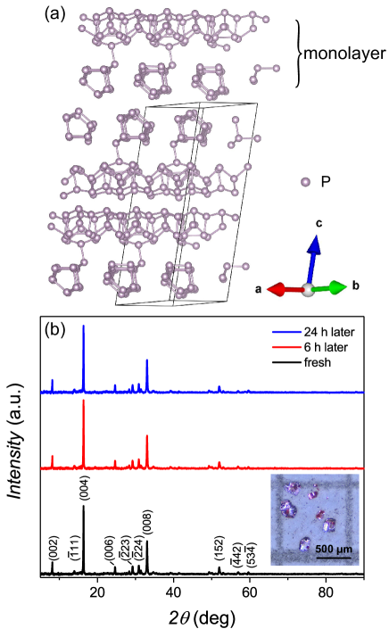
Monoclinic VP belongs to space-group (No. 13) and has a more complex atomic arrangement compared to BP 16.2020 ; 27.2022 . The layered structure of VP is sketched in Fig. 1(a), which also clearly displays one monolayer 21.1969 . Due to the small size of the single crystals (the inset of Fig. 1(b)), obtaining a high-resolution XRD pattern of the natural or cleaved (00) plane is challenging. Therefore, some small pieces of VP single crystals were crushed into powder for XRD measurement. Figure 1(b) displays the XRD patterns during different time of exposure to air for the VP powder. One can see that there is no impure phase and VP is stable in air for at lease one day. Nevertheless, we completed the DAC assembly within 6 h to ensure the high purity of VP sample.
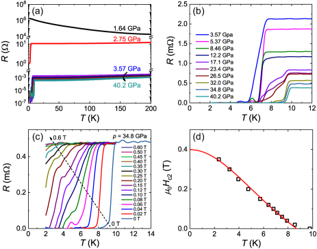
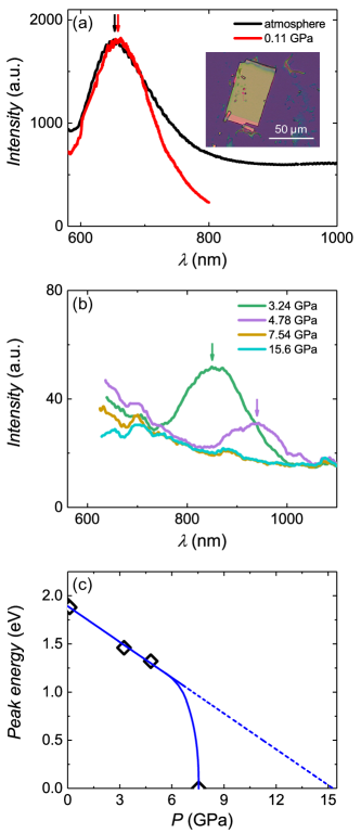
Figure 2(a) shows the temperature dependence of resistance () for VP under pressures up to 40.2 GPa. At 1.64 GPa, the () curve still manifests an insulating behavior. When pressure is increased to 2.75 GPa, a large resistance drop at 4.3 K is observed, indicating the emergence of superconductivity. With further increasing pressure, zero resistance is obtained at low temperatre. In Fig. 2(b), the low-temperature superconducting transitions are plotted for pressures between 3.57 and 40.2 GPa. As the pressure increases, the normal-state resistance deceases monotonically, and the transition temperature c increases from 7.3 to 9.8 K. Here, c is defined as the 10 drop of the normal-state resistance (c10%). At 17.1 GPa, the transition becomes broad and shows steps. This usually implies the coexistence of different superconducting phases 22.2021 ; 23.2011 ; 24.2017 , likely owing to the - structural transition of VP and some degree of pressure inhomogeneity. Above 32.0 GPa, this broadening and the step transition disappear, with c slightly shifting to 9.8 K. From 32.0 to 40.2 GPa, c almost saturates in the structure.
The low-temperature superconducting transitions in different magnetic fields under the pressure of 34.8 GPa are plotted in Fig. 2(c). The transition is gradually suppressed to lower temperature with increasing the field and it completely vanishes in 0.50 T. The temperature dependence of the upper critical field () at 34.8 GPa is summarized in Fig. 2(d). The data can be well fitted by the empirical Ginzburg-Landau (GL) formula and the is determined to be 0.40 T.
The superconducting transition is occasionally accompanied by a structural transition. In the case of BP, the superconductivity is observed at the critical pressure of - structural transition 10.2017 . For VP, it remains the structure until 7.44 GPa and a phase transition from semiconducting structure to metallic structure occurs between 7.44 - 8.49 GPa, as demonstrated by the pressure-dependent Raman spectroscopy 17.2021 . Different from BP, we find that the superconducting transition in VP occurs at 2.75 GPa, well below the critical pressure of - structural transition.
To confirm the order of superconducting and structural phase transitions in VP, PL spectra under various pressures are measured, as shown in Figs. 3(a) and 3(b). PL spectroscopy is an ubiquitous tool used to study exciton emission in semiconductor and the emission energy is usually termed as optical band gap. Hence, PL spectroscopy is widely employed to probe the band structures 27.2022 ; 26.2010 . As seen in Figs. 3(a) and 3(b), a prominent PL peak for VP flake (99 layers) is detected with the maximum intensity at 653 nm (1.9 eV) under ambient pressure, which is consistent with previously reported optical band gap in 29-layer VP thin flake 27.2022 . The detected peak energy is corresponding to the indirect band gap of VP. The assembly of DAC generates a small pressure of 0.11 GPa, making the PL peak slightly red-shifted. Upon further compression, the PL peak shifts to 850 (1.46 eV) and 940 nm (1.32 eV) under 3.24 and 4.78 GPa, respectively. The pressure dependence of the peak energy is given in Fig. 3(c). The peak energy shows a linear dependence at low pressures and the coefficient is estimated to be 0.124 eV/GPa, which is smaller than that of BP 20.2021 ; 99.2001 . As shown in Fig. 3(b), the optical band gap in VP exists until 4.78 GPa, suggesting that the phase transition from semiconducting structure to metallic structure has not occurred under this pressure. Therefore, we confirm that VP exhibits superconductivity in the well-defined structure at 2.75 GPa.
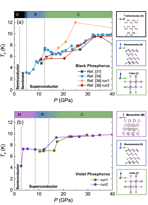
While both VP and BP are forms of phosphorus and exhibit superconductivity under pressure, they have different superconducting phase diagrams under pressure, as plotted in Fig. 4. BP has three discernible states under pressure from the electronic behavior: semiconducting, semimetallic and superconducting states (Fig. 4(a)). At 1.2 GPa, BP undergoes a transition from semiconducting to semimetallic state 9.2015 ; 12.2016 ; 11.2018 . Superconductivity occurs at 5 GPa with a c of 3.2 K, coinciding with the - structural transition 23.1963 ; 6.1984 ; 28.1985 ; 29.2002 ; 10.2017 . Then the c gradually increases to about 10 K before finally saturating above 30 GPa 6.1984 ; 28.1985 ; 29.2002 ; 10.2017 ; 39.2017 . In contrast, VP manifests semiconducting and superconducting states upon compression (Fig. 4(b)). Superconductivity appears at 2.75 GPa in the structure, with a c of 4.3 K. c then increases to 7.3 K and stays constant over a broad pressure range from 3.57 to 12.2 GPa, during which VP undergoes the - structural transition at 8.5 GPa. At 17.1 GPa, c jumps to 9.4 K in the structure. Thus VP has a higher c than BP at low pressure, and both of them show a saturated c at 10 K at high pressure above 30 GPa.
In summary, we have performed high-pressure resistance measurements on the vdW semiconductor VP up to 40.2 GPa. It is found that superconductivity with c 4.3 K emerges at a pressure of 2.75 GPa, well before the - structure transition. This is confirmed by our PL spectroscopy measurements. From 3.57 to 12.2 GPa, c stays at a plateau of 7 K across the - structural transition. Then, c increased to another plateau of 10 K in the structure at 17.1 GPa, and remains this saturation up to 40.2 GPa. Sucn an superconducting phase diagrma under pressure is different from its sister compound BP, which deserves further theoretical and experimental studies to clarify the origin.
This work was supported by the Natural Science Foundation of China (Grant No. 12174064), the National Key Research and Development Program of China (Grant No. 2021YFA1400100), and the Shanghai Municipal Science and Technology Major Project (Grant No. 2019SHZDZX01). Part of the experimental work has been carried out in Fudan Nanofabrication Laboratory. We thank Nanjing 2DNANO Tech. Co., Ltd. for providing us violet phosphorus single crystals.
∗ These authors contributed equally to this work.
† E-mail: syhuang@fudan.edu.cn
‡ E-mail: shiyanlifudan.edu.cn
References
- (1) L. Li, Y. Yu, G. J. Ye, Q. Ge, X. Ou, H. Wu, D. Feng, X. H. Chen, and Y. Zhang, Black phosphorus field-effect transistors, Nat. Nanotechnol. 9, 372 (2014).
- (2) X. Han, Ductile van der Waals materials, Science 369, 509 (2020).
- (3) V. Tran, R. Soklaski, Y. Liang, and L. Yang, Layer-controlled band gap and anisotropic excitons in few-layer black phosphorus, Phys. Rev. B 89, 235319 (2014).
- (4) S. Das, W. Zhang, M. Demarteau, A. Hoffmann, M. Dubey, and A. Roelofs, Tunable transport gap in phosphorene, Nano Lett. 14, 5733 (2014).
- (5) X. Chen, X. Lu, B. Deng, O. Sinai, Y. Shao, C. Li, S. Yuan, V. Tran, K. Watanabe, T. Taniguchi, D. Naveh, L. Yang, and F. Xia, Widely tunable black phosphorus mid-infrared photodetector, Nat. Commun. 8, 1672 (2017).
- (6) J. Qiao, X. Kong, Z.-X. Hu, F. Yang, and W. Ji, High-mobility transport anisotropy and linear dichroism in few-layer black phosphorus, Nat. Commun. 5, 4475 (2014)
- (7) A. N. Rudenko, S. Brener, and M. I. Katsnelson, Intrinsic charge carrier mobility in single-layer black phosphorus, Phys. Rev. Lett. 116, 246401 (2016).
- (8) F. Xia, H. Wang, and Y. Jia, Rediscovering black phosphorus as an anisotropic layered material for optoelectronics and electronics, Nat. Commun. 5, 4458 (2014).
- (9) X. Wang, A. M. Jones, K. L. Seyler, V. Tran, Y. Jia, H. Zhao, H. Wang, L. Yang, X. Xu, and F. Xia, Highly anisotropic and robust excitons in monolayer black phosphorus, Nat. Nanotechnol. 10, 517 (2015).
- (10) X. Ling, S. Huang, E. H. Hasdeo, L. Liang, W. M. Parkin, Y. Tatsumi, A. R. T. Nugraha, A. A. Puretzky, P. M. Das, B. G. Sumpter, D. B. Geohegan, J. Kong, R. Saito, M. Drndic, V. Meunier, and M. S. Dresselhaus, Anisotropic electron-photon and electron-phonon interactions in black phosphorus, Nano Lett. 16, 2260 (2016).
- (11) A. Carvalho, M. Wang, X. Zhu, A. S. Rodin, H. Su, and A. H. Castro Neto, Phosphorene: From theory to applications, Nat. Rev. Mater. 1, 16061 (2016).
- (12) J. O. Island, G. A. Steele, H. S. J. van der Zant, and A. Castellanos-Gomez, Environmental instability of few-layer black phosphorus, 2D Mater. 2, 011002 (2015).
- (13) Y. Y. Illarionov, M. Waltl, G. Rzepa, J.-S. Kim, S. Kim, A. Dodabalapur, D. Akinwande, and T. Grasser, Long-term stability and reliability of black phosphorus field-effect transistors, ACS Nano 10, 9543 (2016).
- (14) L. Zhang, H. Huang, B. Zhang, M. Gu, D. Zhao, X. Zhao, L. Li, J. Zhou, K. Wu, Y. Cheng, and J. Zhang, Structure and properties of violet phosphorus and its phosphorene exfoliation, Angew. Chem., Int. Ed. 59, 1074 (2020).
- (15) Y. Li, S. Cai, W. K. Lai, C. Wang, L. Rogée, L. Zhuang, L. Zhai, S. Lin, M. Li, and S. P. Lau, Impurity-induced robust trionic effect in layered violet phosphorus, Adv. Optical Mater. 10, 2101538 (2022).
- (16) L. Zhang, X. Li, F. Yao, L. Li, H. Huang, X. Zhao, S. Liu, Y. Cheng, H. Xu, and J. Zhang, Fast identification of the crystallographic orientation of violet phosphorus nanoflakes with preferred in-plane cleavage edge orientation, Adv. Funct. Mater. 32, 2111057 (2022).
- (17) A. G. Ricciardulli, Y. Wang, S. Yang, and P. Samorì, Two-dimensional violet phosphorus: A p-type semiconductor for (opto)electronics, J. Am. Chem. Soc. 144, 3660 (2022).
- (18) G. Schusteritsch, M. Uhrin, and C. J. Pickard, Single-layered Hittorf¡¯s phosphorus: A wide-bandgap high mobility 2D material, Nano Lett. 16, 2975 (2016).
- (19) Y. Xu, Q. Long, D. Li, and P. Li, 2D violet phosphorene with highly anisotropic mobility and its vdW heterojunction design for device applications, Phys. Chem. Chem. Phys. 24, 3379 (2022).
- (20) H. Hegger, C. Petrovic, E. G. Moshopoulou, M. F. Hundley, J. L. Sarrao, Z. Fisk, and J. D. Thompson, Pressure-induced superconductivity in quasi-2D CeRhIn5, Phys. Rev. Lett. 84, 4986 (2000).
- (21) Z. Chi, X. Chen, F. Yen, F. Peng, Y. Zhou, J. Zhu, Y. Zhang, X. Liu, C. Lin, S. Chu, Y. Li, J. Zhao, T. Kagayama, Y. Ma, and Z. Yang, Superconductivity in pristine 2-MoS2 at ultrahigh pressure, Phys. Rev. Lett. 120, 037002 (2018).
- (22) T. E. Weller, M. Ellerby, S. S. Saxena, R. P. Smith, and N. T. Skipper, Superconductivity in the intercalated graphite compounds C6Yb and C6Ca, Nat. Phys. 1, 39 (2005).
- (23) R. P. Smith, T. E. Weller, C. A. Howard, M. P. M. Dean, K. C. Rahnejat, S. S. Saxena, and M. Ellerby, Superconductivity in graphite intercalation compounds, Physica C 514, 50 (2015).
- (24) F. Withers, O. Del Pozo-Zamudio, A. Mishchenko, A. P. Rooney, A. Gholinia, K. Watanabe, T. Taniguchi, S. J. Haigh, A. K. Geim, A. I. Tartakovskii, and K. S. Novoselov, Light-emitting diodes by band-structure engineering in van der Waals heterostructures, Nat. Mater. 14, 301 (2015).
- (25) A. Mishchenko, J. S. Tu, Y. Cao, R. V. Gorbachev, J. R. Wallbank, M. T. Greenaway, V. E. Morozov, S. V. Morozov, M. J. Zhu, S. L. Wong, F. Withers, C. R. Woods, Y-J. Kim, K. Watanabe, T. Taniguchi, E. E. Vdovin, O. Makarovsky, T. M. Fromhold, V. I. Fal’ko, A. K. Geim, L. Eaves, and K. S. Novoselov, Twist-controlled resonant tunnelling in graphene/boron nitride/graphene heterostructures, Nat. Nanotechnol. 9, 808 (2014).
- (26) J. T. Ye, Y. J. Zhang, R. Akashi, M. S. Bahramy, R. Arita, and Y. Iwasa, Superconducting dome in a gate-tuned band insulator, Science 338, 1193 (2012).
- (27) W. Shi, J. Ye, Y. Zhang, R. Suzuki, M. Yoshida, J. Miyazaki, N. Inoue, Y. Saito, and Y. Iwasa, Superconductivity series in transition metal dichalcogenides by ionic gating, Sci. Rep. 5, 12534 (2015).
- (28) J. A. Flores-Livas, L. Boeri, A. Sanna, G. Profeta, R. Arita, and M. Eremets, A perspective on conventional high-temperature superconductors at high pressure: Methods and materials, Phys. Rep. 856, 1 (2020).
- (29) L. Zhang, Y. Wang, J. Lv, and Y. Ma, Materials discovery at high pressures, Nat. Rev. Mater. 2, 17005 (2017).
- (30) J. C. Jamieson, Crystal structures adopted by black phosphorus at high pressures, Science 139, 1291 (1963).
- (31) M. Karuzawa, M. Ishizuka, and S. Endo, The pressure effect on the superconducting transition temperature of black phosphorus, J. Phys.: Condens. Matter 14, 10759 (2002).
- (32) H. Kawamura, I. Shirotani, and K. Tachikawa, Anomalous superconductivity in black phosphorus under high pressures, Solid State Commun. 49, 879 (1984).
- (33) H. Kawamura, I. Shirotani, and K. Tachikawa, Anomalous superconductivity and pressure induced phase transitions in black phosphorus, Solid State Commun. 54, 775 (1985).
- (34) J. Guo, H. Wang, F. von Rohr, W. Yi, Y. Zhou, Z. Wang, S. Cai, S. Zhang, X. Li, Y. Li, J. Liu, K. Yang, A. Li, S. Jiang, Q. Wu, T. Xiang, R. J. Cava, and L. Sun, Electron-hole balance and the anomalous pressure-dependent superconductivity in black phosphorus, Phys. Rev. B 96, 224513 (2017).
- (35) Z. J. Xiang, G. J. Ye, C. Shang, B. Lei, N. Z. Wang, K. S. Yang, D. Y. Liu, F. B. Meng, X. G. Luo, L. J. Zou, Z. Sun, Y. Zhang, and X. H. Chen, Pressure-induced electronic transition in black phosphorus, Phys. Rev. Lett. 115, 186403 (2015).
- (36) P.-L. Gong, D.-Y. Liu, K.-S. Yang, Z.-J. Xiang, X.-H. Chen, Z. Zeng, S.-Q. Shen, and L.-J. Zou, Hydrostatic pressure induced three-dimensional Dirac semimetal in black phosphorus, Phys. Rev. B 93, 195434 (2016).
- (37) P. Di Pietro, M. Mitrano, S. Caramazza, F. Capitani, S. Lupi, P. Postorino, F. Ripanti, B. Joseph, N. Ehlen, A. Grneis, A. Sanna, G. Profeta, P. Dore, and A. Perucchi, Emergent Dirac carriers across a pressure-induced Lifshitz transition in black phosphorus, Phys. Rev. B 98, 165111 (2018).
- (38) J. A. Flores-Livas, A. Sanna, A. P. Drozdov, L. Boeri, G. Profeta, M. Eremets, and S. Goedecker, Interplay between structure and superconductivity: Metastable phases of phosphorus under pressure, Phys. Rev. Mater. 1, 024802 (2017).
- (39) L. Zhang, H. Huang, Z. Lv, L. Li, M. Gu, X. Zhao, B. Zhang, Y. Cheng, and J. Zhang, Phonon properties of bulk violet phosphorus single crystals: Temperature and pressure evolution, ACS Appl. Electron. Mater. 3, 1043 (2021).
- (40) H. Thurn and H. Krebs, ber struktur und eigenschaften der halbmetalle. XXII. Die kristallstruktur des Hittorfschen phosphors, Acta Crystallogr. Sect. B 25, 125 (1969).
- (41) K. Zhang, M. Xu, N. Li, M. Xu, Q. Zhang, E. Greenberg, V. B. Prakapenka, Y.-S. Chen, M. Wuttig, H.-K. Mao, and W. Yang, Superconducting phase induced by a local structure transition in amorphous Sb2Se3 under high pressure, Phys. Rev. Lett. 127, 127002 (2021).
- (42) M. Sakata, Y. Nakamoto, K. Shimizu, T. Matsuoka, and Y. Ohishi, Superconducting state of Ca-VII below a critical temperature of 29 K at a pressure of 216 GPa, Phys. Rev. B 83, 220512(R) (2011).
- (43) E. Greenberg, B. Hen, S. Layek, I. Pozin, R. Friedman, V. Shelukhin, Y. Rosenberg, M. Karpovski, M. P. Pasternak, E. Sterer, Y. Dagan, G. K. Rozenberg, and A. Palevski, Superconductivity in multiple phases of compressed GeSb2Te4, Phys. Rev. B 95, 064514 (2017).
- (44) A. Splendiani, L. Sun, Y. Zhang, T. Li, J. Kim, C.-Y. Chim, G. Galli, and F. Wang, Emerging photoluminescence in monolayer MoS2, Nano Lett. 10, 1271 (2010).
- (45) Y. Akahama and H. Kawamura, Optical and electrical studies on band-overlapped metallization of the narrow-gap semiconductor black phosphorus with layered structure, Phys. Stat. Sol. (B) 223, 349 (2001).
- (46) S. Huang, Y. Lu, F. Wang, Y. Lei, C. Song, J. Zhang, Q. Xing, C. Wang, Y. Xie, L. Mu, G. Zhang, H. Yan, B. Chen, and H. Yan, Layer-dependent pressure effect on the electronic structure of 2D black phosphorus, Phys. Rev. Lett. 127, 186401 (2021).