Isotropic plasma-thermal atomic layer etching of superconducting TiN films using sequential exposures of molecular oxygen and SF6/H2 plasma
Abstract
Microwave loss in superconducting TiN films is attributed to two-level systems in various interfaces arising in part from oxidation and microfabrication-induced damage. Atomic layer etching (ALE) is an emerging subtractive fabrication method which is capable of etching with Angstrom-scale etch depth control and potentially less damage. However, while ALE processes for TiN have been reported, they either employ HF vapor, incurring practical complications; or the etch rate lacks the desired control. Further, the superconducting characteristics of the etched films have not been characterized. Here, we report an isotropic plasma-thermal TiN ALE process consisting of sequential exposures to molecular oxygen and an SF6/H2 plasma. For certain ratios of SF6:H2 flow rates, we observe selective etching of TiO2 over TiN, enabling self-limiting etching within a cycle. Etch rates were measured to vary from 1.1 Å/cycle at 150 °C to 3.2 Å/cycle at 350 °C using ex-situ ellipsometry. We demonstrate that the superconducting critical temperature of the etched film does not decrease beyond that expected from the decrease in film thickness, highlighting the low-damage nature of the process. These findings have relevance for applications of TiN in microwave kinetic inductance detectors and superconducting qubits.
I Introduction
Titanium nitride (TiN) is a superconducting metal of interest for microelectronics and superconducting quantum devices. Its high kinetic inductance, low microwave loss, and high absorption coefficient in the infrared and optical frequencies make it a promising material for single photon detectors [1, 2], ultra-sensitive current detectors [3], quantum-limited parametric amplifiers [4], and qubits [5, 6]. Superconducting microwave resonators based on TiN routinely exhibit internal quality factors Qi [6, 7, 2]. TiN is also used for microelectronic applications in which it is used as a copper diffusion barrier and metal gate electrode [8, 9, 10]. In many of these applications, imperfections at film interfaces are the primary limitation to figures of merit for various devices. For instance, the quality factor of superconducting microresonators is presently thought to be limited by microwave surface loss associated with two-level systems (TLS) in various interfaces [11, 12, 13]. Subtractive nanofabrication methods based on typical wet or dry etching processes are unsuitable for mitigating TLS density in these devices due to the lack of Angstrom-scale precision in etching and the sub-surface damage they induce [14, 15, 16].
Atomic layer etching (ALE) is an emerging subtractive nanofabrication process with potential to overcome these limitations [17, 18, 19]. Early forms of ALE focused on directional etching [20, 21]. Directional ALE is based on surface modification by adsorption of a reactive species, and subsequent sputtering of the modified surface with ions or neutral atoms of low energy exceeding only the sputtering threshold of the modified surface [22, 23]. Isotropic thermal ALE processes have also been developed recently using sequential, self-limiting surface chemical reactions [24]. In thermal ALE, the material surface is modified to form a stable layer that can then be removed by a selective mechanism, such as temperature cycling, ligand-exchange transmetalation reactions, or others [25, 18]. Isotropic thermal and plasma ALE processes have now been reported for various dielectrics and semiconductors including Al2O3 [26, 27], SiO2 [28, 29], AlN [30, 31, 32], InGaAs [33, 34] and others [35, 36, 37, 18]. Surface smoothing of etched surfaces using ALE has also been reported for various metals and semiconductors [26, 38, 34, 39].
For TiN, ALE processes based on fluorination and ligand exchange with Sn(acac)2, trimethylaluminum (TMA), dimethylaluminum chloride (DMAC), and SiCl4 did not lead to etching [40]. When fluorinated, TiN retains its 3+ oxidation state, yielding TiF3. TiF3 either formed non-volatile ligand-exchange products or did not react with the precursors, and hence no etching occurred. This difficulty was overcome by first converting the Ti to the 4+ oxidation state with exposure to ozone or H2O2, which upon fluorination using HF produced volatile TiF4 [41]. A conceptually similar process has also been reported using O2 plasma and CF4 plasma [42].
Despite these advances, limitations remain. The use of HF vapor incurs practical complications. The process of Ref. [42] based on O2 plasma and CF4 requires a heating and cooling step per cycle which can lead to impractical time per cycle on most conventional plasma tools. Additionally, the recipe achieves nm/cycle etch rates, which lacks the desired Angstrom-scale control and low damage characteristics. Previous reports did not examine the effects of ALE on the superconducting properties of the samples. Identifying alternate reactants to HF vapor while maintaining Angstrom-level precision over the thickness, and ensuring that superconducting properties are not degraded, all remain topics of interest for TiN ALE.
Here, we report the isotropic atomic layer etching of TiN using sequential exposures of O2 gas and SF6/H2 plasma. The process is based on the selective etching of TiO2 over TiN for certain ratios of SF6:H2. The observed etch rates varied from 1.1 Å/cycle up to 3.2 Å/cycle for temperatures between 150 °C and 350 °C respectively, as measured using ex-situ ellipsometry. The etched surface was found to exhibit a % decrease in surface roughness. The superconducting transition temperature was unaffected by ALE beyond the expected change due to the decrease in film thickness, highlighting the low-damage nature of the process. Our findings indicate the potential of ALE in the processing of TiN for superconducting quantum electronics and microelectronics applications.
II Experiment
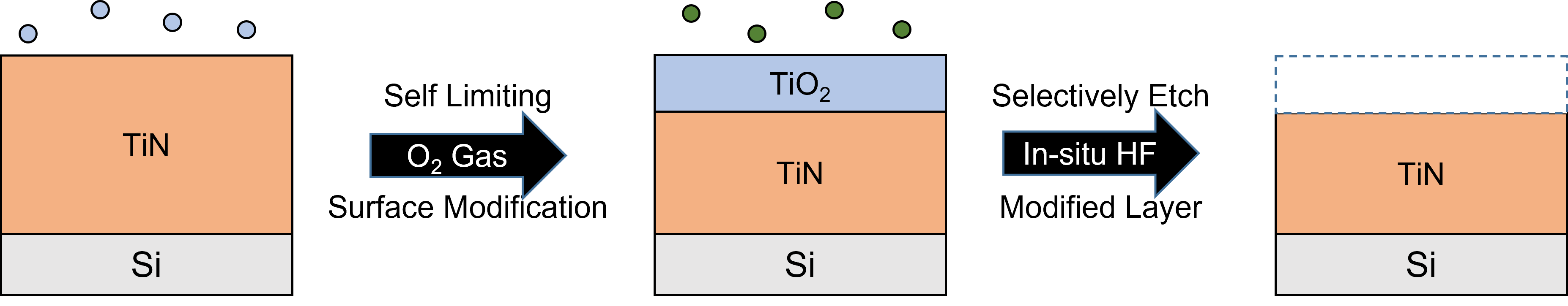
The plasma-thermal ALE process of this work is illustrated in Figure 1. An exposure of molecular oxygen was used to oxidize the surface of TiN to TiO2, followed by a purge. After, a mixture of SF6 and H2 gas was introduced into the chamber and ignited to form SF6/H2 plasma. After this exposure, the reactor was again purged to complete the cycle. The use of SF6/H2 plasma was motivated by noting that HF does not etch TiN, but fluorine radicals will spontaneously etch TiN [41, 43]. Studies on SiN and Si etching using hydrogen and fluorine-containing plasma have shown that the plasma formed by the mixture yields different products at different plasma concentration ratios, including HF molecules at high hydrogen concentrations [44, 45, 46]. We therefore hypothesize that at high H2 concentrations, the SF6/H2 plasma forms molecular HF which then selectively etches the TiO2 over the TiN, with minimal spontaneous etching from F radicals. The formation of HF in the SF6/H2 plasma is referred to as “in-situ HF” throughout the paper.
We investigated this approach to ALE of TiN using an Oxford Instruments FlexAL atomic layer deposition (ALD) system with an inductively-coupled plasma source, as described in Refs. [47, 48]. The substrate table temperature varied between 150 °C to 200 °C, as measured by the FlexAL substrate table thermometer. Prior to introducing the sample into the chamber for etching, the chamber walls and carrier wafer were conditioned by coating with 50 nm of Al2O3 using 300 cycles of Al2O3 ALD [48]. Alumina was selected as it does not form volatile fluoride species on exposure to SF6 plasma. For TiN ALE, the sample was first exposed to 50 sccm O2 and 50 sccm Ar gas for 2 s at 100 mTorr pressure, followed by a 10 s purge. Next, a mixture of 20 sccm H2 and 4 sccm SF6 was stabilized at 100 mTorr for 5 s before striking the plasma at 100 W for 10 s. The excess reactants were purged for 10 s before repeating the cycle. The recipe resulted in a total time of s per cycle. Before the sample was moved to the loadlock, the chamber was pumped down for 60 s. The sample was additionally held in the loadlock for two hours to cool down before exposure to air, so as to reduce oxygen diffusion into the sample.
The film thickness before and after etching was measured by ex-situ spectroscopic ellipsometry (J.A. Woolam M2000) at and from 370 nm to 1000 nm. Thickness was determined using 5 points on a 5 5 mm2 square array. Subsequently, the data were fit using a Lorentz model to obtain the thickness of the samples [49, 41]. Reported thickness values are the average of the 5 points. XPS analysis was performed using a Kratos Axis Ultra x-ray photoelectron spectrometer using a monochromatic Al K source. Depth profiling was performed using an Ar ion beam with a 60 s interval for each cycle. The estimated milling depth was calculated based on initial and final film thickness measured by ex-situ ellipsometry and assuming a constant ion milling rate. The XPS data was analyzed in CASA-XPS from Casa Software Ltd. We adopt universal Tougaard background and sub-peak fitting routines from Refs. [50, 51].
The film surface topography was characterized using a Bruker Dimension Icon atomic force microscope (AFM) over a m2 area. The raw height maps collected on the AFM were processed by removing tilt via linear plane-fit. The surface roughness and power spectral density (PSD) were computed from the plane-fit height maps using procedures outlined in previous literature [39, 52]. The PSD provides a quantitative measure of the lateral distance over which the surface profile varies in terms of spatial frequencies [53, 52]. The PSD was calculated by taking the absolute square of the normalized 1D-discrete Fourier transform of each row and column from the plane-fit AFM scan. The transformed data was then averaged to produce a single PSD curve. Reported roughness values and PSD curves were found to be consistent across 3 spots on each film.
Electrical resistivity measurements were performed on the Quantum Design DynaCool Physical Property Measurement System (PPMS). The TiN films were connected to the PPMS sample holder by four aluminum wires, wirebonded on the Westbond 7476D Wire Bonder. The film resistivity was measured using a 4-point setup [7]. The resistivity was measured from 6 K to 1.7 K, and the data was used to calculate the superconducting critical temperature () of the films.
The samples consisted of 50 – 60 nm thick TiN films on high resistivity Si (100) wafers (cm, UniversityWafer) prepared using ALD with the same FlexAL system. The ALD process consisted of sequential half-cycles of exposure to tetrakis(dimethylamino)titanium (TDMAT) and nitrogen plasma with a 20 W DC bias at 350 °C, similar to the procedure reported in Refs. [7, 54]. The resistance at 6 K and of a 60 nm thick ALD TiN film were measured to be cm and K, respectively; these values are comparable to those reported for other TiN films made using TDMAT [7, 55, 54]. The chemical composition of the deposited films are described in Section III.5. The titania (TiO2) films used for demonstrating etch selectivity in Section III.1 were made by oxidizing TiN samples under an oxygen plasma for 5 minutes at 300 °C, yielding a 5 nm thick TiO2 film on top of the TiN film. The thicknesses of the TiO2 films were measured using ex-situ ellipsometry.
III Results
III.1 Selective etching with SF6/H2 Plasma
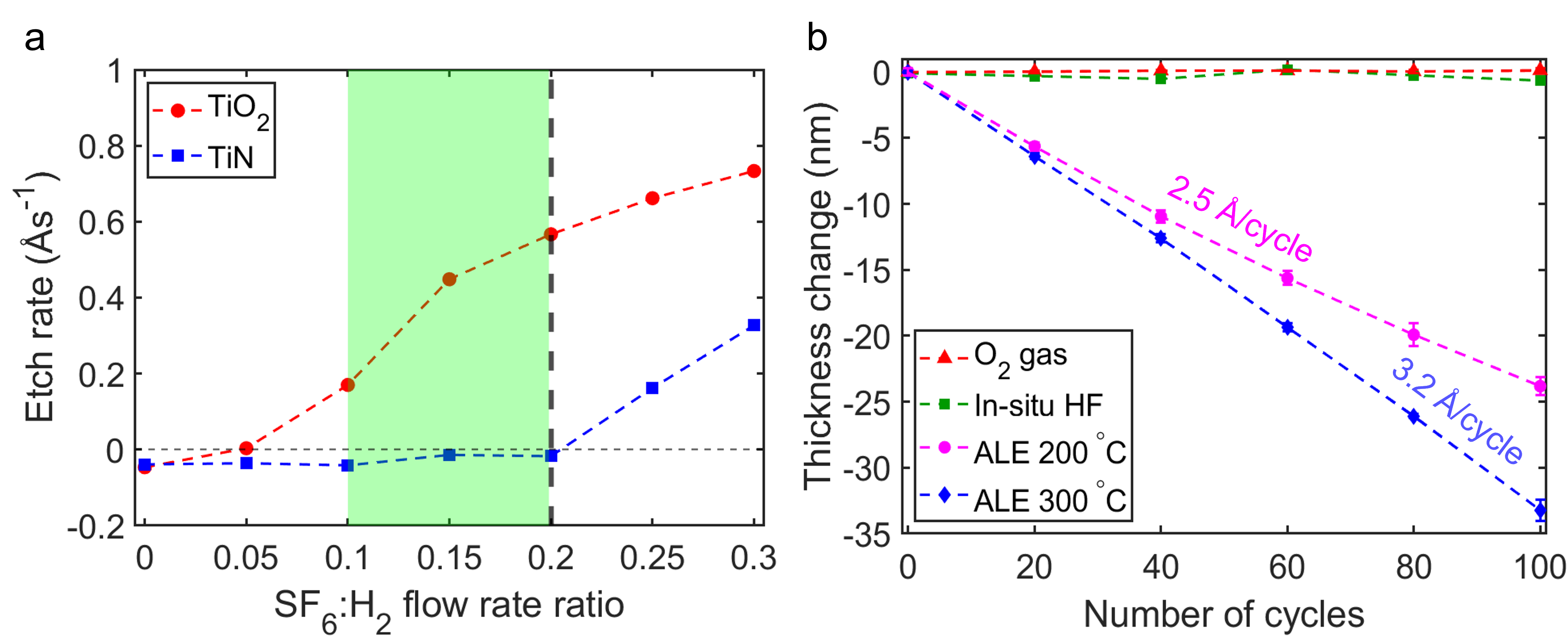
We begin by examining the etch rate of TiO2 and TiN films for various SF6:H2 flow rate ratios, . Figure 2 shows the etch rates of TiN and TiO2 versus at 300 °C. For , negligible etching of either film is observed. Negative etch rates correspond to an increase in the thickness of the film, which we assume to be growth of non-volatile TiF3. For , we observe spontaneous etching of TiO2, with the etch rate monotonically increasing with . For TiN, we observe no etching for , but for etching occurs. We attribute these observations to the formation of in-situ HF along with negligible fluorine radical concentration for , similar to the results obtained in prior work [44, 45, 46]. For , the concentration of F radicals becomes sufficient to spontaneously etch the TiN, leading to increasing etch rates for both films. From our measurements, we find that achieves selective etching of TiO2 over TiN. To obtain the highest etch selectivity of TiO2 over TiN, we select for our experiments. This 1:5 ratio of SF6:H2 plasma is used throughout the rest of the paper.
III.2 TiN ALE using O2 and in-situ HF exposures
Figure 2 shows the thickness change of TiN versus number of cycles for both half cycles, and for the full ALE recipe at 200 °C and 300 °C. For the half-cycles, the thickness change was measured after exposure to only molecular oxygen or in-situ HF. No etching was observed for either half-cycle, supporting the need for both steps. In contrast, we observe a decrease in the thickness with increasing number of cycles when using both steps. The etch rate is calculated by dividing the total thickness change by the number of cycles, giving values of Å/cycle at 200 °C and Å/cycle at 300 °C.
We further examine the effect of temperature on the etch rate. Figure 3 shows the etch per cycle (EPC) versus table temperature ranging from 150 °C and 350 °C. The etch rates are calculated over a 100 cycles using a linear fit. We find that the etch rate increases from 1.1 Å/cycle at 150 °C to 3.2 Å/cycle at 300 °C. The increase in EPC with temperature is similar to what has been observed in previous thermal ALE studies of various materials [41, 42, 18, 56]. We also observe a constant etch rate from 300 °C to 350 °C, similar to what is reported in Figure 7 of Ref. [41].
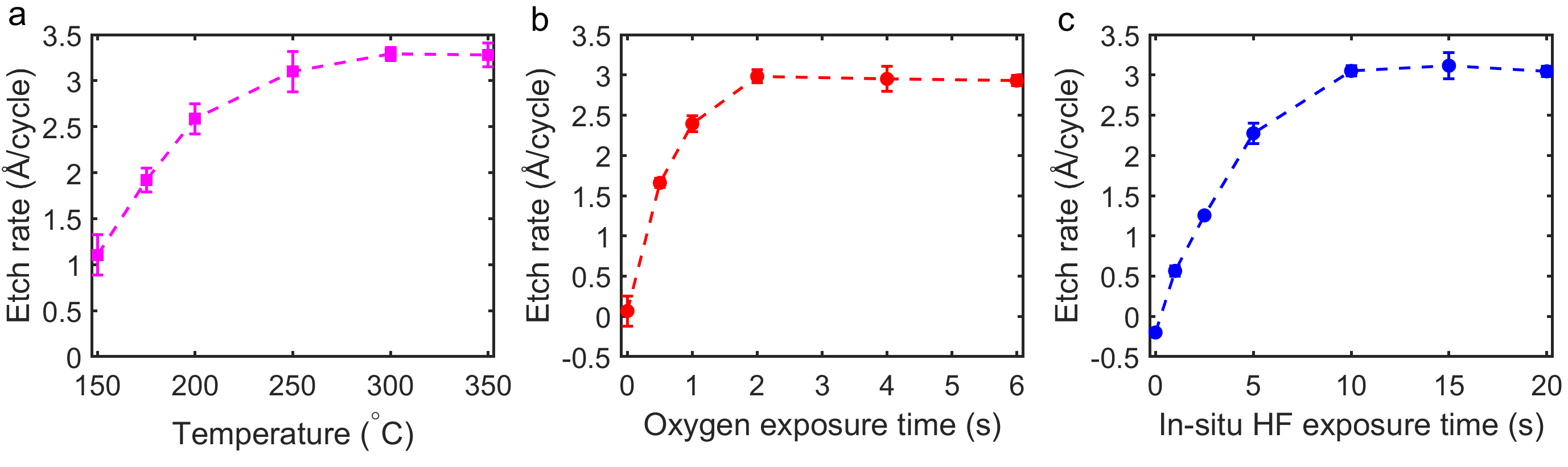
We also explored the self-limiting nature of the recipe by measuring the saturation curves of each half-cycle. For each saturation curve, the purge times and one half-cycle time are fixed while the other is varied. The etch rates reported are calculated based on the thickness change over 50 cycles at 300 °C. In Figure 3, the in-situ HF step is fixed at 10 s, while the etch rate is measured versus the oxygen exposure time. The etch rate is observed to saturate to Å/cycle above 2 s, which is consistent with the self-limiting nature of the oxidation step. In Figure 3, the oxidation step is fixed at 2 s, while the etch rate is measured versus in-situ HF exposure time. The etch rate saturates to Å/cycle above 10 s, which is consistent with the selectivity of the in-situ HF to etch TiO2 and terminate on the TiN.
III.3 Characterization of film composition
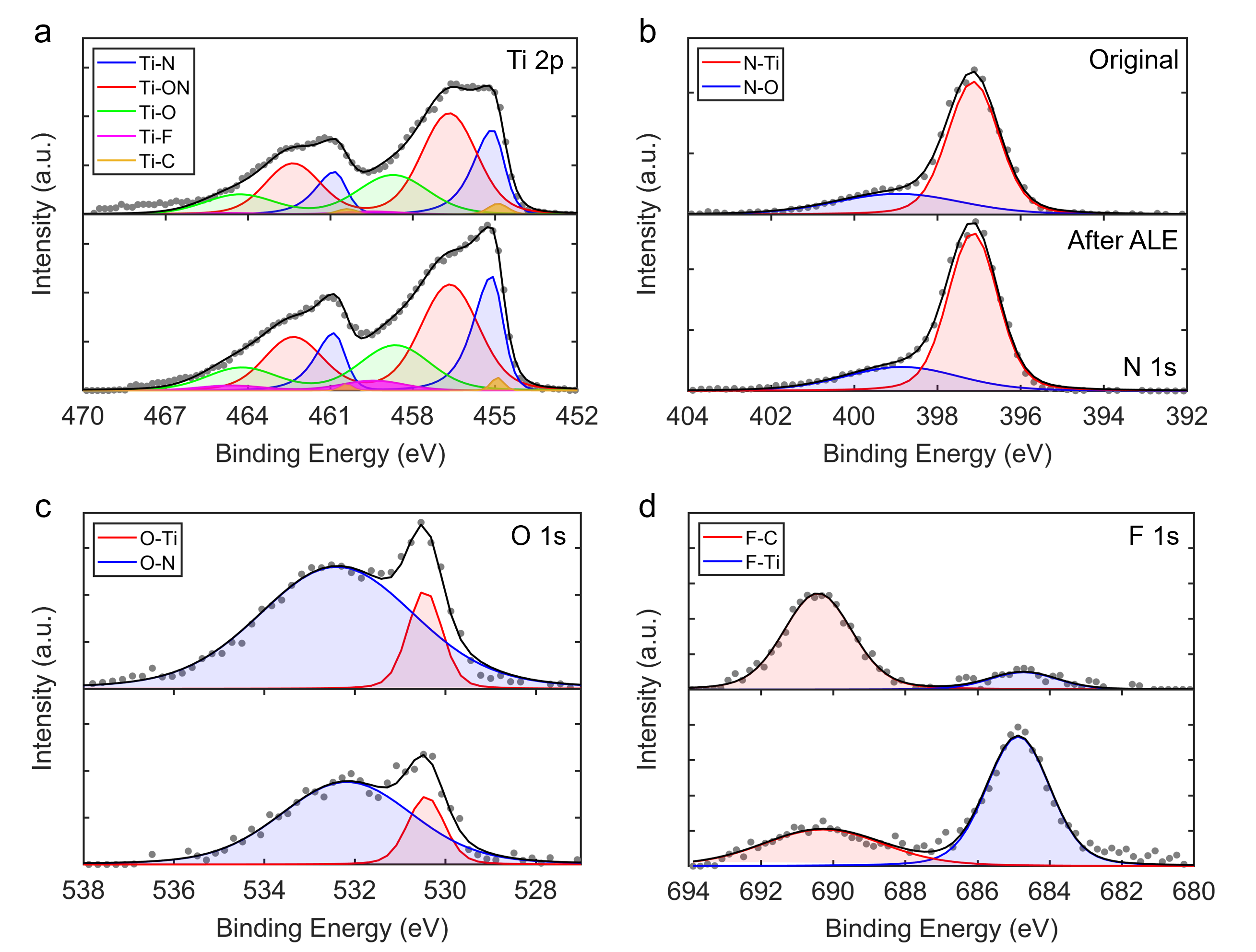
We next characterize the chemical composition of the TiN films before and after ALE using XPS. In Figure 4, we show the core levels of Ti2p, N1s, O1s, C1s and F1s. For the Ti2p XPS spectra in Figure 4, we observe five components. Each component is a doublet consisting of a 2p3/2 and a 2p1/2 subpeak. We observe subpeaks corresponding to Ti-C (454.9 eV and 460.4 eV) [57, 58, 59], Ti-N (455.1 eV and 460.8 eV) [60, 61, 62], Ti-ON (456.5 eV and 462.3 eV) [60, 61, 62], Ti-O (458.5 eV and 464.2 eV) [60, 61, 62], and Ti-F (459.4 eV and 465.6 eV) [63, 64]. In Figure 4, we report the N1s spectra with two subpeaks at 397.1 eV and 398.9 eV, belonging to N-Ti and N-O bonds, respectively [60, 61, 62]. In Figure 4, we report the O1s spectra with two subpeaks at 530.4 eV and 532.2 eV, corresponding to O-Ti and O-N bonds, respectively [60, 61, 62]. In Figure 4, we report the F1s spectra with two subpeaks at 684.9 eV and 690.3 eV, corresponding to F-Ti and F-C bonds, respectively [63, 65, 64].
We observe that the Ti2p spectra is dominated by oxides and oxynitrides, consistent with the presence of a native oxide on TiN [55, 61]. After ALE (bottom panels of Figures 4, 4 and 4), an increase in the magnitude of the Ti-N and N-Ti peaks is observed along with an overall decrease in the O1s peak magnitude. The decreased O1s signal implies a reduced native oxide concentration after ALE, as has been observed in other works [31, 66, 67]. The F1s spectra for the original sample may be attributed to contamination from using the same chamber for deposition and etching, which is consistent with the reduced magnitude of the F1s peak in the original sample compared to that in the ALE-treated sample (bottom panel of Figure 4).
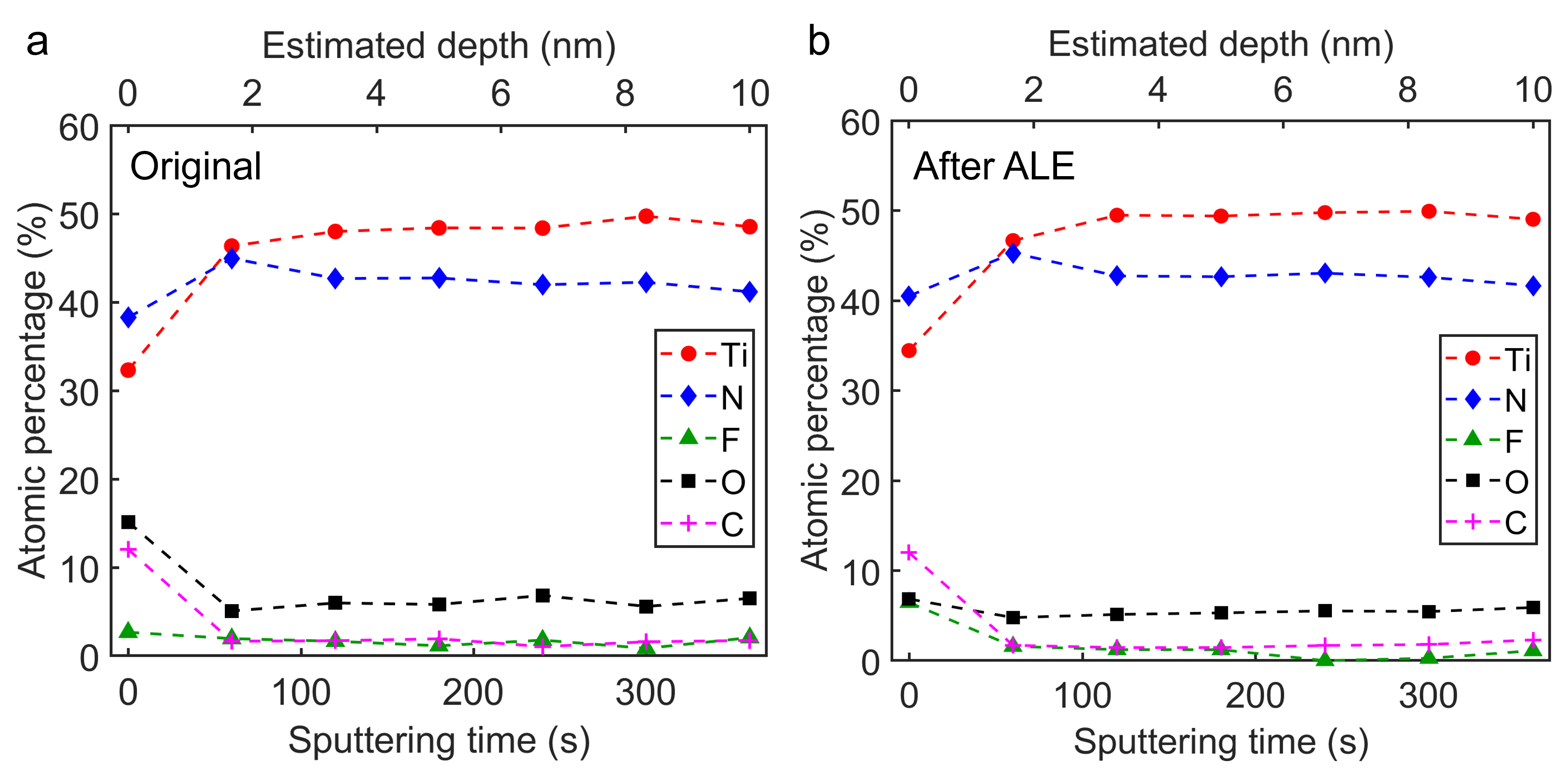
We also performed depth-profiling XPS to determine the atomic concentrations on the surface and bulk. In Figure 5, we show the atomic concentrations of Ti, N, F, C and O as a function of sputtering time and estimated depth in the original and ALE-treated films. In the original sample (Figure 5), the atomic concentrations on the surface are 31.9% (Ti), 37.6% (N), 16.1% (O), 12.0% (C), and 2.4% (F). After 120 s Ar milling , the atomic concentrations plateau to their bulk values of 48.6% (Ti), 42.3% (N), 6.1% (O), 1.9% (C), and 1.1% (F). The carbon and oxygen levels are consistent with other reported ALD TiN films made using TDMAT [55, 68, 69]. For the ALE-treated sample (Figure 5), the atomic concentrations on the surface are 34.2% (Ti), 39.5% (N), 7.9% (O), 11.9% (C), and 6.5% (F). After 120 s Ar milling , the atomic concentrations plateau to their bulk values of 49.0% (Ti), 42.2% (N), 5.9% (O), 1.8% (C), and 1.1% (F). We observe a decrease in the surface oxygen concentration in the ALE-treated film. An increase in the surface fluorine concentration of the ALE-treated film is also observed, consistent with other works involving the interactions of fluorine-containing plasma with dielectric films [70, 31]. The atomic concentrations in the bulk of the ALE-treated film are within 95% of the values in the original film. Therefore, we conclude that the effect of ALE is confined to a few nanometers of the surface, with negligible effect on the bulk chemical composition.
III.4 Surface roughness characterization
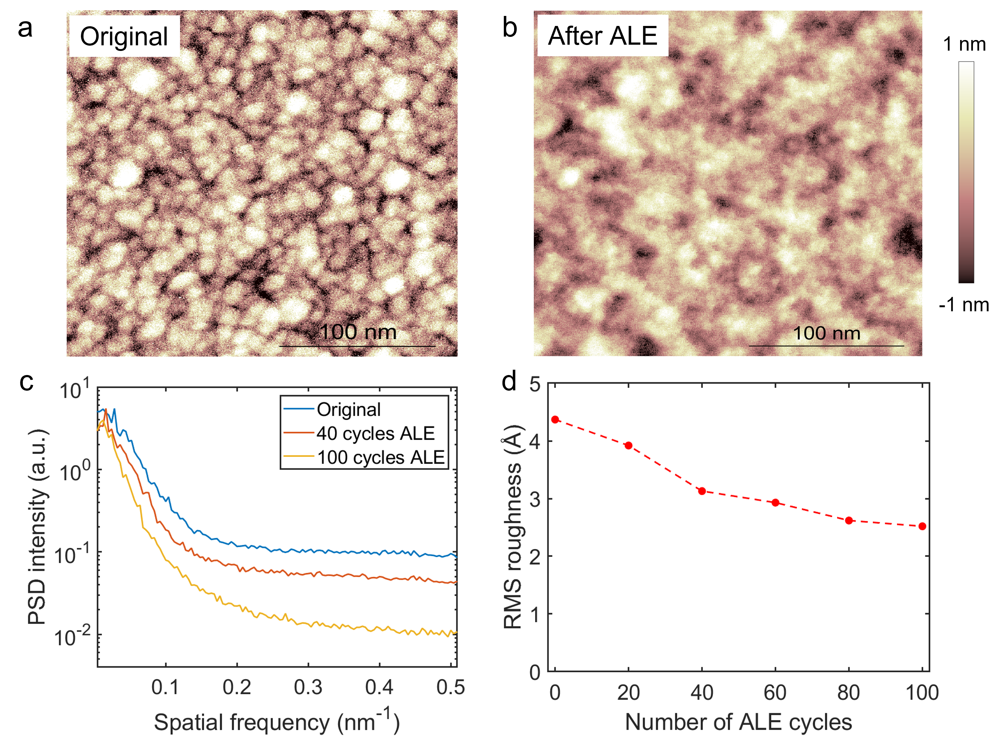
We characterized the roughness of the TiN films before and after ALE using AFM. Figure 6 shows the plane-fit height map of the film as deposited using ALD. Figure 6 shows the plane-fit height map after 100 cycles of ALE at 300 °C. Figure 6 shows the PSD curves for the original film, after 40 ALE cycles and after 100 ALE cycles at 300 °C. We observe a decrease in the PSD intensity across all length scales as the number of ALE cycles is increased, indicating that features with length scales from nm are smoothed by the ALE process. In Figure 6, the RMS roughness is plotted versus the number of ALE cycles at 300 °C. We observe a monotonic decrease in RMS roughness from 4.4 Å to 2.5 Å after 100 cycles. This 43% reduction in roughness was observed across 3 different positions on the sample.
III.5 Electrical and superconducting properties
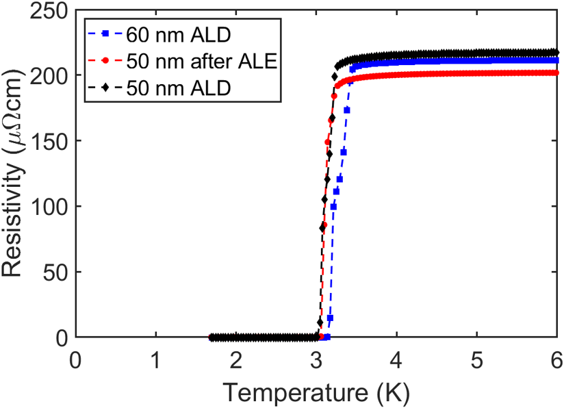
We investigated the effect of ALE on the electrical and superconducting properties of the TiN films by measuring their resistivity from 6 K to 1.7 K. A 60 nm TiN film was deposited using ALD, which was etched to 50 nm using ALE. Another 50 nm TiN film was prepared using ALD to compare to the ALE-treated 50 nm film. The measured resistivity versus temperature for the three films is shown in Figure 7. The resistivity at 6 K of the 60 nm ALD film is found to be cm, with a superconducting critical temperature K. The resistivity of the TiN film is consistent with those previously reported for ALD TiN films [7, 55], and the reported is similar to the of other TiN films grown with TDMAT [7, 71]. After 40 cycles of ALE at 200 °C, the TiN thickness decreased to 50 nm, with a resistivity of cm at 6 K and K. For comparison, the 50 nm ALD film had a resistivity of cm at 6 K, and K. We therefore find that the change in of the TiN film after ALE is consistent with that expected with a decrease of 10 nm in thickness, without any additional decrease due to process-induced damage. This observation highlights the improved quality of the processed films compared to those obtained from processing methods which lack atomic control [72]. The reduced 6 K resistivity of the ALE-treated film is thought to arise due to the removal of the native oxide. This result warrants further investigation and is a topic of future study.
IV Discussion
We now discuss the characteristics of our plasma-thermal TiN ALE process in context with isotropic thermal ALE processes for TiN and related materials. Thermal ALE of TiN has been reported using molecular O3 or H2O2 and HF vapor [41], and O2 plasma and CF4 plasma [42]. The first process leads to an etch per cycle (EPC) of 0.20 Å/cycle at 200 °C, achieving atomic-scale control of etching. However, the recipe requires the use of HF vapor which incurs practical complications. The second process based on O2 plasma and CF4 plasma achieves an EPC of 17.1 Å/cycle at 200 °C, which is a larger EPC than is desired for manipulating the surface region of the films. The second process also requires an additional heating step, which can lead to impractical process times on conventional tools. The present recipe achieves an EPC of 2.6 Å/cycle at 200 °C and 3.1 Å/cycle at 250 °C, providing etch rates between the previous reported recipes. The present recipe also avoids the use of HF, requiring only an SF6/H2 plasma that also yields etching selectivity of TiO2 over TiN.
Our isotropic plasma-thermal ALE may find potential applications in the fabrication of TiN-based superconducting microresonators for microwave kinetic inductance detectors and qubits, where the native oxide hosts parasitic TLS that presently limit the device performance. Based on our XPS and resistivity measurements, ALE-treated films have a reduced oxygen concentration while maintaining unaltered bulk chemistry and electrical properties. These properties make ALE promising for reducing the number of TLS in the metal-air interface and thereby improving the quality factor of superconducting microresonators. The smoothing effect and isotropic Angstrom-scale EPC of the present ALE recipe is also relevant for fabricating TiN-based nanoscale metal gate electrodes in CMOS devices and various transistor designs, where the metal layers are required to have thickness on the order of nm with uniformity [9, 73]. The ALD system in our work (Oxford Instruments, FlexAL) has demonstrated high uniformity on 200 mm diameter substrates [48], and therefore our process has the potential to extend to wafer-scale applications.
V Conclusion
We have reported an isotropic plasma-thermal atomic layer etching process for TiN using sequential exposures of molecular oxygen and SF6/H2 plasma. The SF6/H2 plasma selectively etches TiO2 over TiN for SF6:H2 flow rate ratios between 0.1 and 0.2. The etch rate varies from 1.1 Å/cycle at 150 °C to 3.2 Å/cycle at 350 °C. We observe a smoothing effect from ALE, corresponding to a reduction in RMS roughness after 100 cycles. The surface oxygen concentration is reduced by after 100 cycles of ALE, indicating a decrease in the volume of surface oxide. We also find that ALE does not induce any change in beyond that expected from the decrease in film thickness, highlighting the low-damage nature of the process. We anticipate that the ability to engineer the surface of TiN films on the Angstrom-scale using isotropic ALE will facilitate applications of TiN in superconducting resonators and microelectronics.
VI Acknowledgements
This work was supported by NSF under Award #2234390. The authors thank Nicholas Chittock (Eindhoven University of Technology) for useful discussions, and Phillipe Pearson (California Institute of Technology) for assistance with the wirebonder. We gratefully acknowledge the critical support and infrastructure provided for this work by The Kavli Nanoscience Institute and the Molecular Materials Research Center of the Beckman Institute at the California Institute of Technology.
References
- Leduc et al. [2010] H. G. Leduc, B. Bumble, P. K. Day, B. H. Eom, J. Gao, S. Golwala, B. A. Mazin, S. McHugh, A. Merrill, D. C. Moore, O. Noroozian, A. D. Turner, and J. Zmuidzinas, Appl. Phys. Lett. 97, 10.1063/1.3480420 (2010).
- Vissers et al. [2010] M. R. Vissers, J. Gao, D. S. Wisbey, D. A. Hite, C. C. Tsuei, A. D. Corcoles, M. Steffen, and D. P. Pappas, Appl. Phys. Lett. 97, 10.1063/1.3517252 (2010).
- Kher et al. [2016] A. Kher, P. K. Day, B. H. Eom, J. Zmuidzinas, and H. G. Leduc, J. Low Temp. Phys. 184, 480 (2016).
- Ho Eom et al. [2012] B. Ho Eom, P. K. Day, H. G. LeDuc, and J. Zmuidzinas, Nat. Phys. 8, 623 (2012).
- Hazard et al. [2019] T. M. Hazard, A. Gyenis, A. Di Paolo, A. T. Asfaw, S. A. Lyon, A. Blais, and A. A. Houck, Phys. Rev. Lett. 122, 010504 (2019).
- Chang et al. [2013] J. B. Chang, M. R. Vissers, A. D. Córcoles, M. Sandberg, J. Gao, D. W. Abraham, J. M. Chow, J. M. Gambetta, M. Beth Rothwell, G. A. Keefe, M. Steffen, and D. P. Pappas, Appl. Phys. Lett. 103, 10.1063/1.4813269 (2013).
- Shearrow et al. [2018] A. Shearrow, G. Koolstra, S. J. Whiteley, N. Earnest, P. S. Barry, F. J. Heremans, D. D. Awschalom, E. Shirokoff, and D. I. Schuster, Appl. Phys. Lett. 113, 10.1063/1.5053461 (2018).
- Kim [2003] H. Kim, Journal of Vacuum Science & Technology B: Microelectronics and Nanometer Structures Processing, Measurement, and Phenomena 21, 2231 (2003).
- Zhao and Xiang [2019] C. Zhao and J. Xiang, Appl. Sci. 9, 2388 (2019).
- Lima et al. [2012] L. P. B. Lima, M. A. Moreira, J. A. Diniz, and I. Doi, Phys. Status Solidi C 9, 1427 (2012).
- Gao et al. [2007] J. Gao, J. Zmuidzinas, B. A. Mazin, H. G. LeDuc, and P. K. Day, Appl. Phys. Lett. 90, 10.1063/1.2711770 (2007).
- Barends et al. [2008] R. Barends, H. L. Hortensius, T. Zijlstra, J. J. A. Baselmans, S. J. C. Yates, J. R. Gao, and T. M. Klapwijk, Appl. Phys. Lett. 92, 10.1063/1.2937837 (2008).
- Gao et al. [2008] J. Gao, M. Daal, A. Vayonakis, S. Kumar, J. Zmuidzinas, B. Sadoulet, B. A. Mazin, P. K. Day, and H. G. Leduc, Appl. Phys. Lett. 92, 10.1063/1.2906373 (2008).
- Sandberg et al. [2012] M. Sandberg, M. R. Vissers, J. S. Kline, M. Weides, J. Gao, D. S. Wisbey, and D. P. Pappas, Appl. Phys. Lett. 100, 10.1063/1.4729623 (2012).
- Altoé et al. [2022] M. V. P. Altoé, A. Banerjee, C. Berk, A. Hajr, A. Schwartzberg, C. Song, M. Alghadeer, S. Aloni, M. J. Elowson, J. M. Kreikebaum, E. K. Wong, S. M. Griffin, S. Rao, A. Weber-Bargioni, A. M. Minor, D. I. Santiago, S. Cabrini, I. Siddiqi, and D. F. Ogletree, PRX Quantum 3, 020312 (2022).
- Gao et al. [2022] R. Gao, W. Yu, H. Deng, H.-S. Ku, Z. Li, M. Wang, X. Miao, Y. Lin, and C. Deng, Phys. Rev. Mater. 6, 036202 (2022).
- Lill et al. [2016] T. Lill, K. J. Kanarik, S. Tan, M. Shen, E. Hudson, Y. Pan, J. Marks, V. Vahedi, and R. A. Gottscho, in Encyclopedia of Plasma Technology (CRC Press, Boca Raton, FL, USA, 2016) pp. 133–142.
- George [2020] S. M. George, Acc. Chem. Res. 53, 1151 (2020).
- Sang et al. [2020] X. Sang, Y. Xia, P. Sautet, and J. P. Chang, J. Vac. Sci. Technol., A 38, 043005 (2020).
- Sakaue et al. [1990] H. Sakaue, S. Iseda, K. Asami, J. Yamamoto, M. Hirose, and Y. Horiike, Jpn. J. Appl. Phys. 29, 2648 (1990).
- Horiike et al. [1990] Y. Horiike, T. Tanaka, M. Nakano, S. Iseda, H. Sakaue, A. Nagata, H. Shindo, S. Miyazaki, and M. Hirose, J. Vac. Sci. Technol., A 8, 1844 (1990).
- Kanarik et al. [2015] K. J. Kanarik, T. Lill, E. A. Hudson, S. Sriraman, S. Tan, J. Marks, V. Vahedi, and R. A. Gottscho, J. Vac. Sci. Technol., A 33, 020802 (2015).
- Oehrlein et al. [2015] G. S. Oehrlein, D. Metzler, and C. Li, ECS J. Solid State Sci. Technol. 4, N5041 (2015).
- George and Lee [2016] S. M. George and Y. Lee, ACS Nano 2016, ,5 (2016).
- Osakada [2003] K. Osakada, in Current Methods in Inorganic Chemistry, Vol. 3 (Elsevier, Walthm, MA, USA, 2003) pp. 233–291.
- Zywotko et al. [2018] D. R. Zywotko, J. Faguet, and S. M. George, J. Vac. Sci. Technol., A 36, 10.1116/1.5043488 (2018).
- Lee et al. [2015a] Y. Lee, J. W. DuMont, and S. M. George, Chem. Mater. 27, 3648 (2015a).
- DuMont et al. [2017] J. W. DuMont, A. E. Marquardt, A. M. Cano, and S. M. George, ACS Appl. Mater. Interfaces 9, 10296 (2017).
- Rahman et al. [2018] R. Rahman, E. C. Mattson, J. P. Klesko, A. Dangerfield, S. Rivillon-Amy, D. C. Smith, D. Hausmann, and Y. J. Chabal, ACS Appl. Mater. Interfaces 10, 31784 (2018).
- Johnson et al. [2016] N. R. Johnson, H. Sun, K. Sharma, and S. M. George, J. Vac. Sci. Technol., A 34, 10.1116/1.4959779 (2016).
- Wang et al. [2023] H. Wang, A. Hossain, D. Catherall, and A. J. Minnich, J. Vac. Sci. Technol., A 41, 10.1116/6.0002476 (2023).
- Cano et al. [2022] A. M. Cano, A. Lii-Rosales, and S. M. George, J. Phys. Chem. C 126, 6990 (2022).
- Lu et al. [2019] W. Lu, Y. Lee, J. C. Gertsch, J. A. Murdzek, A. S. Cavanagh, L. Kong, J. A. del Alamo, and S. M. George, Nano Lett. 19, 5159 (2019).
- Ohba et al. [2017] T. Ohba, W. Yang, S. Tan, K. J. Kanarik, and K. Nojiri, Jpn. J. Appl. Phys. 56, 06HB06 (2017).
- Lee et al. [2015b] Y. Lee, J. W. DuMont, and S. M. George, ECS J. Solid State Sci. Technol. 4, N5013 (2015b).
- Fang et al. [2018] C. Fang, Y. Cao, D. Wu, and A. Li, Progress in Natural Science: Materials International 28, 667 (2018).
- Fischer et al. [2021] A. Fischer, A. Routzahn, S. M. George, and T. Lill, J. Vac. Sci. Technol., A 39, 10.1116/6.0000894 (2021).
- Kanarik et al. [2017] K. J. Kanarik, S. Tan, W. Yang, T. Kim, T. Lill, A. Kabansky, E. A. Hudson, T. Ohba, K. Nojiri, J. Yu, R. Wise, I. L. Berry, Y. Pan, J. Marks, and R. A. Gottscho, J. Vac. Sci. Technol., A 35, 10.1116/1.4979019 (2017).
- Gerritsen et al. [2022] S. H. Gerritsen, N. J. Chittock, V. Vandalon, M. A. Verheijen, H. C. M. Knoops, W. M. M. Kessels, and A. J. M. Mackus, ACS Appl. Nano Mater. 5, 18116 (2022).
- Lee et al. [2016] Y. Lee, C. Huffman, and S. M. George, Chem. Mater. 28, 7657 (2016).
- Lee and George [2017] Y. Lee and S. M. George, Chem. Mater. 29, 8202 (2017).
- Shim et al. [2022] D. Shim, J. Kim, Y. Kim, and H. Chae, Journal of Vacuum Science & Technology B, Nanotechnology and Microelectronics: Materials, Processing, Measurement, and Phenomena 40, 022208 (2022).
- Pearton et al. [1991] S. J. Pearton, A. Katz, and A. Feingold, Semicond. Sci. Technol. 6, 830 (1991).
- Pankratiev et al. [2020] P. A. Pankratiev, Y. V. Barsukov, A. A. Kobelev, A. Y. Vinogradov, I. V. Miroshnikov, and A. S. Smirnov, J. Phys. Conf. Ser. 1697, 012222 (2020).
- Volynets et al. [2020] V. Volynets, Y. Barsukov, G. Kim, J.-E. Jung, S. K. Nam, K. Han, S. Huang, and M. J. Kushner, J. Vac. Sci. Technol., A 38, 023007 (2020).
- Jung et al. [2020] J.-E. Jung, Y. Barsukov, V. Volynets, G. Kim, S. K. Nam, K. Han, S. Huang, and M. J. Kushner, J. Vac. Sci. Technol., A 38, 10.1116/1.5125569 (2020).
- Coumou et al. [2012] P. C. J. J. Coumou, M. R. Zuiddam, E. F. C. Driessen, P. J. de Visser, J. J. A. Baselmans, and T. M. Klapwijk, IEEE Trans. Appl. Supercond. 23, 7500404 (2012).
- van Hemmen et al. [2007] J. L. van Hemmen, S. B. S. Heil, J. H. Klootwijk, F. Roozeboom, C. J. Hodson, M. C. M. van de Sanden, and W. M. M. Kessels, J. Electrochem. Soc. 154, G165 (2007).
- Langereis et al. [2006] E. Langereis, S. B. S. Heil, M. C. M. van de Sanden, and W. M. M. Kessels, J. Appl. Phys. 100, 10.1063/1.2214438 (2006).
- Jaeger and Patscheider [2012] D. Jaeger and J. Patscheider, J. Electron Spectrosc. Relat. Phenom. 185, 523 (2012).
- Maarouf et al. [2021] M. Maarouf, M. B. Haider, Q. A. Drmosh, and M. B. Mekki, Crystals 11, 239 (2021).
- Jacobs et al. [2017] T. D. B. Jacobs, T. Junge, and L. Pastewka, Surf. Topogr. Metrol. Prop. 5, 013001 (2017).
- Elson and Bennett [1995] J. M. Elson and J. M. Bennett, Appl. Opt. 34, 201 (1995).
- Faraz et al. [2018] T. Faraz, H. C. M. Knoops, M. A. Verheijen, C. A. A. van Helvoirt, S. Karwal, A. Sharma, V. Beladiya, A. Szeghalmi, D. M. Hausmann, J. Henri, M. Creatore, and W. M. M. Kessels, ACS Appl. Mater. Interfaces 10, 13158 (2018).
- Musschoot et al. [2009] J. Musschoot, Q. Xie, D. Deduytsche, S. Van den Berghe, R. L. Van Meirhaeghe, and C. Detavernier, Microelectron. Eng. 86, 72 (2009).
- Chittock et al. [2020] N. J. Chittock, M. F. J. Vos, T. Faraz, W. M. M. E. Kessels, H. C. M. Knoops, and A. J. M. Mackus, Appl. Phys. Lett. 117, 10.1063/5.0022531 (2020).
- Santerre et al. [1999] F. Santerre, M. A. El Khakani, M. Chaker, and J. P. Dodelet, Appl. Surf. Sci. 148, 24 (1999).
- Näslund et al. [2020] L.-Å. Näslund, P. O. Å. Persson, and J. Rosen, J. Phys. Chem. C 124, 27732 (2020).
- Luthin and Linsmeier [2001] J. Luthin and Ch. Linsmeier, Physica Scripta 91, 134 (2001).
- Kuznetsov et al. [1992] M. V. Kuznetsov, Ju. F. Zhuravlev, V. A. Zhilyaev, and V. A. Gubanov, J. Electron Spectrosc. Relat. Phenom. 58, 1 (1992).
- Saha and Tompkins [1992] N. C. Saha and H. G. Tompkins, J. Appl. Phys. 72, 3072 (1992).
- Chan and Lu [2009] M.-H. Chan and F.-H. Lu, Thin Solid Films 517, 5006 (2009).
- Mousty-Desbuquoit et al. [1987] C. Mousty-Desbuquoit, J. Riga, and J. J. Verbist, Inorg. Chem. 26, 1212 (1987).
- Natu et al. [2021] V. Natu, M. Benchakar, C. Canaff, A. Habrioux, S. Célérier, and M. W. Barsoum, Matter 4, 1224 (2021).
- Beamson and Briggs [1993] G. Beamson and D. Briggs, High Resolution XPS of Organic Polymers: The Scienta ESCA300 Database (1993).
- Hennessy et al. [2017] J. Hennessy, C. S. Moore, K. Balasubramanian, A. D. Jewell, K. France, and S. Nikzad, J. Vac. Sci. Technol., A 35, 10.1116/1.4986945 (2017).
- Metzler et al. [2017] D. Metzler, C. Li, C. S. Lai, E. A. Hudson, and G. S. Oehrlein, J. Phys. D: Appl. Phys. 50, 254006 (2017).
- Fillot et al. [2005] F. Fillot, T. Morel, S. Minoret, I. Matko, S. Maîtrejean, B. Guillaumot, B. Chenevier, and T. Billon, Microelectron. Eng. 82, 248 (2005).
- Elam et al. [2003] J. W. Elam, M. Schuisky, J. D. Ferguson, and S. M. George, Thin Solid Films 436, 145 (2003).
- Fischer et al. [2017] A. Fischer, R. Janek, J. Boniface, T. Lill, K. J. Kanarik, Y. Pan, V. Vahedi, and R. A. Gottscho, in Proceedings Volume 10149, Advanced Etch Technology for Nanopatterning VI, Vol. 10149 (SPIE, 2017) pp. 20–24.
- Proslier et al. [2011] T. Proslier, J. Klug, N. C. Becker, J. W. Elam, and M. Pellin, ECS Trans. 41, 237 (2011).
- Zheng et al. [2022] K. Zheng, D. Kowsari, N. J. Thobaben, X. Du, X. Song, S. Ran, E. A. Henriksen, D. S. Wisbey, and K. W. Murch, Appl. Phys. Lett. 120, 10.1063/5.0082755 (2022).
- Matsukawa et al. [2015] T. Matsukawa, K. Endo, H. Akasaka, Y. Kamiya, M. Ikeda, K. Tsunekawa, T. Nakagawa, Y. X. Liu, and M. Masahara, in 2015 Silicon Nanoelectronics Workshop (SNW) (IEEE, Japan, 2015) pp. 1–2.