Chiplet Cloud: Building AI Supercomputers for Serving Large Generative Language Models
Abstract.
Large language models (LLMs) such as OpenAI’s ChatGPT and GPT-4 have demonstrated the unprecedented capabilities of autoregressive generation in multiple AI tasks, triggering disruptive technology innovations around the world. However, with the increase of model size and context length, and the slowdown of Moore’s Law, it becomes increasingly challenging to serve these large models efficiently on existing cloud hardware platforms that are powered by TPUs and GPUs. Hardware inefficiency has become a major factor limiting the democratization of LLMs.
In this paper, we propose Chiplet Cloud, a chiplet-based ASIC AI-supercomputer architecture that optimizes total cost of ownership (TCO) per generated token for serving large generative language models to reduce the overall cost to deploy and run these applications in the real world. The Chiplet Cloud architecture utilizes a unique approach to scale-up cloud computing by leveraging thousands of replicated chiplet accelerator modules to collaboratively perform token generation at an unprecedented TCO per token. A key architectural feature to achieve this is the ability to fit all model parameters inside the on-chip SRAMs of the chiplets to eliminate bandwidth limitations. Doing so is non-trivial as the amount of memory required is very large and growing for modern LLMs. This has led to larger chips with worse die yield and server level thermal dissipation thus increasing the total cost of the system. By using chiplets, we can moderate the die size to improve the system cost while leveraging software mappings to exploit parallelism found within the computation to overcome the potential data communication overhead.
To explore the software-hardware co-design space and perform software mapping -aware Chiplet Cloud optimizations across the architectural design space, we propose a comprehensive design methodology that not only accurately explores a spectrum of major design trade-offs in the joint space of hardware and software, but also generates a detailed performance-cost analysis on all valid design points and then outputs the Pareto frontier. We design and evaluate Chiplet Cloud on four popular LLMs on the market representing a range of model sizes. Compared to A100 GPU clouds and TPUv4 clouds, our results show that Chiplet Cloud can achieve up to 94 and 15 improvement in TCO/Token respectively. This significantly reduces the cost for realistically serving modern LLMs.
1. Introduction
Over the past few months, a new generative Large Language Model (LLM) called ChatGPT (OpenAI, 2022) has gained significant attention around the world due to its unprecedented ability to perform a variety of natural language tasks. Compared with the previous language models, ChatGPT is much better at understanding user intent, generating human-like responses, and keeping multi-round conversations coherent with context. While the technology behind ChatGPT is impressive, it is the way it exposed LLMs in a way that was useful for the general population and introduced a new business model for these AI systems that has sent a shock wave of excitement throughout the technology industry. Since ChatGPT, we have already seen several announcements of LLM being integrated with other services such as web search, word processing, and programming IDEs (GitHub, 2023). LLMs are currently driving a technology revolution at planet-scale, changing the way we interact with AI models on a daily basis.
Much of the transformational increase in ML capabilities comes from the unprecedented scale of the LLMs being deployed. For example, ChatGPT is based on OpenAI’s GPT-3.5, an updated version of GPT-3 (Brown et al., 2020) and one of the most powerful large language models available at the time of deployment. The model is trained on 570GB of text data and has more than 175B parameters, requiring a huge amount of hardware resources for both training and inference. For instance, GPT-3 requires 23 days to train on 1536 A100 GPUs (Narayanan et al., 2021). Inference alone also requires a significant amount of hardware resources, e.g., serving GPT-3 typically requires 8 A100 GPUs simply to satisfy the minimum memory requirements.
Serving generative transformer-based large language models on commodity hardware, like GPUs, is already hitting a scalability wall. State-of-the-art GPT-3 throughput on GPU is 18 tokens/sec per A100 (Aminabadi et al., 2022). ChatGPT and the promise of integrating large-language models into various existing technologies (e.g. web-search) puts into question the scalability and profitability of large-language models. For example, Google Searching processes over 99,000 queries (Mohsin, 2023) per second. If GPT-3 is embedded in every query, and assuming each query generates 500 tokens, Google needs 340,750 NVIDIA DGX servers (2,726,000 A100 GPUs) to keep up. The cost of these GPUs exceeds $40 billion in capital expenditure alone. Energy consumption will also be huge. Assuming a 50% utilization, the average power would be over 1 Gigawatt, which is enough energy to power 750,000 homes. The CO2 emissions of producing 1 Gigawatt are equivalent to the annual emissions of more than 200,000 cars. Hardware inefficiencies will significantly limit the impact of the large generative language models in the future. To address both the high capital expenditure and energy cost of running LLMs, we must design and build hardware systems that attain significantly better total-cost-of-ownership (TCO) per token served.
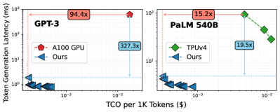
We propose Chiplet Cloud, a chiplet-based ASIC AI-supercomputer architecture for LLMs which aims to reduce the TCO per generated token. Figure 1 shows the TCO/Token and latency Pareto frontier of Chiplet Cloud for GPT-3 (Brown et al., 2020) and PaLM 540B (Chowdhery et al., 2022). Compared to A100 GPU (Aminabadi et al., 2022) and TPUv4 (Pope et al., 2022) clouds, our design achieves up to and TCO/Token improvement respectively. The cost analysis are based on Lambda GPU Cloud (Lambda, 2023) and Google Cloud (Cloud, 2023).
Chiplet Cloud employs a unique scale-up architecture to design a full cloud-scale system for running large generative language models at unrivaled TCO per performance that will drive and enable future LLM applications to run at planet-scale. To achieve this, we aggressively customize the architecture of Chiplet Cloud for the targeted LLMs. Driven by the design trade-offs between cost and performance, the architecture of Chiplet Cloud stores all model parameters and KV values in on-chip SRAM memory (Sec.3.2.1). On-chip memories such as SRAM have better read latency and read/write energy than external memories such as DDR or HBM but require more silicon per bit. We show this design choice wins in the competition of TCO per performance for serving large generative language models but requires careful consideration with respect to the chiplet die size, chiplet memory capacity and total number of chiplets to balance the fabrication cost and model performance (Sec.3.2.2) We observe that the inter-chiplet communication issues can be effectively mitigated through proper software-hardware co-design leveraging mapping strategies such as tensor and pipeline model parallelism (Shoeybi et al., 2020; Narayanan et al., 2021; Pope et al., 2022).
To explore the massive hardware-software co-design space of Chiplet Cloud and find TCO per performance optimal system mapping strategies, we propose a two-phase design-search methodology for hardware exploration and software evaluation. The hardware exploration phase (Sec.4.1) conducts a bottom-up design space exploration of Chiplet Cloud hardware architecture from a flexible accelerator architecture up to a 1U rack mounted server architecture taking power budget, floorplan, and thermal limits into account. The software evaluation phase (Sec.4.2) then performs a detailed performance and TCO analysis of the server designs given a specific workload while simultaneously searching for software mapping strategies that complements the server architecture. While software mapping strategies for LLMs are now considered standard techniques for improving performance on existing hardware platforms, our design methodology flips the order and allows us to explore mapping strategies across all possible Chiplet Cloud hardware platforms to further optimize the TCO per performance capabilities of Chiplet Cloud.
In summary, this paper makes the following contributions:
-
•
We conduct a thorough study on the current hardware limitations for serving generative LLMs and motivate the need of building ASIC supercomputers (Sec.2);
-
•
We propose Chiplet Cloud, a chiplet-based ASIC Supercomputer architecture for serving generative LLMs, aiming at better TCO/Token (Sec.3);
-
•
We present a comprehensive software-hardware co-design methodology that enables an accurate Chiplet Cloud design space exploration with software mapping optimization aware search (Sec.4);
- •
2. Democratizing LLMs Through Specialization
As large generative language models are being widely used in more applications, we are heading towards a scalability wall due to inefficiencies of generalized commodity hardware platforms such as GPUs. This will lead to the cost of running LLMs to increase over time as these workloads grow in scale and complexity leading us to a world where very powerful AI systems are prohibitively expensive to use for the layman. In order to democratize this disruptive technology, specialized hardware will be the best way to go.
The rest of this section is dedicated to a brief background on large generative language models in the context of what makes them difficult to run on modern hardware platforms and how moving to ASIC supercomputers is more financially feasible despite the daunting upfront cost of developing and designing such a machine.
2.1. Large Generative Language Models
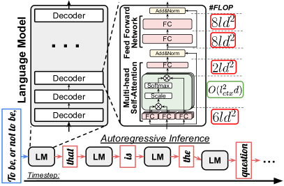
The architecture of a generative language model is shown in the top of Figure 2. The architecture of a generative language model is built around the transformer decode block, with each block defining a layer of the model (Vaswani et al., 2017). Within the decoder layer is a multi-head self attention mechanism followed by a 2-layer feed-forward network. In Figure 2 we show the number of operations for each step of the decode block. For modern large language models, fully connected (FC) layers dominate the runtime of the decode block since the model dimension is much larger than the input length and the context length , thus . For example, more than 99% of MAC operations in GPT-3 are spent on just the FC layers.
Generative language models use autoregressive inference to generate tokens, as shown at the bottom of Figure 2. The first pass through the model takes takes the input sequence as a whole and generates a single output token. That output token is then used as the input for the next pass, continuing until a specific “end of text” token is generated. This dependency between generated tokens poses a challenge for massively parallel LLM inference, limiting system utilization. A common technique used to reduce the amount of computation required for every token generated after the initial input sequence is known as KV caching where intermediate results of the multi-headed self-attention mechanism from previous input tokens are cached and don’t need to be recomputed. The maximum size of the KV cache is dependant on the context length of the model and batch size.
2.2. A High-Performance and More Profitable Hardware Solution: ASIC
In order to run LLMs at scale and achieve high performance and high energy efficiency, we propose building ASIC supercomputers specifically for LLMs. ASICs are known to have the potential to deliver better performance and energy efficiency than CPUs and GPUs, since they are optimized for specific tasks. One major factor limiting the deployment of ASICs is non-recurring engineering (NRE) costs (Khazraee et al., 2017). The barrier for overcoming NRE is primarily about the opportunity cost of running the workload on the current hardware offerings. The difference in TCO between running a workload on an ASIC supercomputer vs the current available hardware platform determines the break even point for NRE, where the NRE cost directly equals the savings from using an ASIC supercomputer. The current cost of running workloads like web search with integrated LLMs is so massive that it not only justifies the cost of creating ASIC super computers but going even further as to co-optimize those super computers for specifics LLMs for additional improvement in the TCO per token.
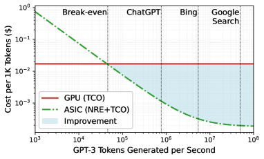
The NRE of ASIC supercomputers includes silicon mask cost, CAD tools, IP licensing, flip-chip BGA packing, server designs, and labor. We extend the NRE model from Moonwalk (Khazraee et al., 2017) to use a 7nm technology node and estimate the NRE of a 7nm ASIC accelerator for large language models to be approximately $35M. In Figure 3, we compare the cost to generate 1K tokens on GPT-3 on modern GPUs clouds vs ASIC supercomputers. The GPU cost is based on the state-of-the-art throughput from DeepSpeed-Inference (Aminabadi et al., 2022)) and the best available rental price of $1.1/GPU/hour from Lambda (Lambda, 2023). The ASIC cost combines the NRE and TCO on a lifetime of 1.5 year, while the performance is based on our TCO optimized Chiplet Cloud. The shaded region shows the saving per 1K tokens switching from GPU to ASIC, with the break-even point for GPT-3 being approximately 46,000 tokens/sec. This shows that the NRE cost of ASIC supercomputers is justifiable for modern workloads and thus customized hardware still remains the best solution to democratize LLMs.
3. Chiplet Cloud: A TCO-Optimized ASIC Architecture for LLMs
This section introduces the architecture and main insights of Chiplet Cloud. Instead of just optimizing raw hardware performance, more companies start to design accelerators for better TCO per performance (Jouppi et al., 2021). TCO of an accelerator consists of the capital expenditures (CapEx, mainly from chip fabrication) and the operation expenditures (OpEx, mainly from power consumption); thus, . We list some of the main challenges of designing ASICs for large generative language models, and give our solutions on how to optimize the TCO per performance. We believe that an architecture that enables these solutions, i.e. Chiplet Cloud, is what is demanded for a large ASIC LLM serving system.
3.1. Main Challenges
3.1.1. Memory Bandwidth Significantly Limits LLMs’ Inference Performance.
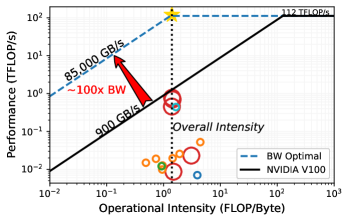
The inference performance of LLMs on GPU is limited by DRAM bandwidth, rather than tensor core utilization. Under smaller batch sizes and normal inference sequence lengths, the performance is limited by the memory bandwidth in reading model parameters, i.e., loading the parameters from HBM to on-chip registers (Aminabadi et al., 2022). This is due to the low operational intensity of GeMM in FC layers, which requires to load new parameter for almost every operation. As we discussed previously, FC layers dominate the computation with small inputs. Under larger batch sizes and long sequence lengths, the memory bandwidth bottleneck occurs when reading KV cache. In this case, KV cache size can be much greater than model parameter size itself. For example, for GPT-3 with a context length of 2K, every input sequence needs 2 GB of KV cache. With the batch size of 256, the KV cache further grows to 512 GB while the total model size is 350 GB. Figure 4 shows the roofline of GPT-2 on a V100 GPU, where most kernels are bounded by the memory bandwidth. To fully utilize the 112 TFLOPS computing power on V100, we need a total bandwidth of 85000 GB/s, which is about of HBM bandwidth. Reducing parameter and KV access latency and power is critical for better TCO/Token in LLM inference.
3.1.2. Chip Costs Dominate TCO
Due to the autoregressive feature of the LLMs, the next token depends on previous generated tokens, which greatly limits the hardware utilization. The best hardware utilization on the state-of-the-art implementation is around 50% (Aminabadi et al., 2022) on GPUs and 40% on TPUs (during the decoding phase) (Pope et al., 2022). Note that these are achieved with a very large batch size (e.g., 1024), the utilization can be as low as 1% when batch sizes are small (e.g., 4) (Pope et al., 2022), which are the most common cases for real-world LLM inference. Another issue with the current systems is that chips used (e.g., A100 and TPUv4) are massive and close to the wafer reticle limit of around 800 mm2, which poses a huge challenge to control the fabrication cost. Under such low utilization and high chip fabrication cost, the capital expenditures will account for a significant portion of the TCO. According to our evaluation, at 50% utilization, an A100 GPU purchased at manufacturer’s suggested retail price has a TCO of 97.7% on CapEx. Even if people tapeout their own GPUs, the CapEx percentage can still be as high as 58.7%. Reducing chip costs will be the key to lower the TCO per generated token.
3.2. Key Architectural Solutions
3.2.1. Design Tradeoffs Driven by TCO per Performance
SRAM has a much higher bandwidth and much lower access energy than external memory such as HBM, but has lower density. To address the memory bandwidth bottleneck, we want to argue that from a better TCO per performance perspective, buffering all model parameters and intermediate data (such as K, V) in on-chip memory such as SRAM is a preferred design option for our case.
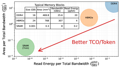
Consider a language model accelerator with die area () and average power (), that provides a total memory bandwidth of . The accelerator’s TCO can be approximately modeled as , where and are constant coefficients. The chip cost actually grows superlinearly with the area. We use a linear model here for simplicity, which will not affect our subsequent analysis. As discussed earlier, since LLM inference is usually memory bandwidth bounded, throughput (token/sec) will be proportional to the bandwidth . As a result, we have . To optimize the TCO/Token, we want a smaller and . Assuming that other modules in the chip remain unchanged, area, read energy, and bandwidth of the the parameter memory will be they key factors that affect this figure of merit. We list typical memory blocks of DDR4, HBM2e and SRAM in the table in Fig. 5, and plot the area per total bandwidth and the read energy per total bandwidth when we use these blocks to store model parameters. Compared with DDR4 and HBM2e, on-chip SRAM has much smaller () and (). Although the same memory technology can have blocks of different sizes, which affects the bandwidth and read energy, the trend shown in Fig. 5 remains the same. For example, SRAM has an order-of-magnitude better area per bandwidth and read energy per bandwidth than DRAM. Thus, although buffering all parameters on-chip requires more silicon, it will likely to reduce the TCO per generated token.
Recently, there has been an industry trend to deploy more on-chip memory on deep learning accelerators to reduce the excessive off-chip memory access. Microsoft’s Brainwave (Fowers et al., 2018) pins DNN model weights in distributed on-chip SRAM. Google’s TPUv4i (Jouppi et al., 2021) contains 144 MB SRAM, and GraphCore’s IPU 2 (Knowles, 2021) has 896 MB SRAM, Adding more on-chip memory to provide higher bandwidth is easier, cheaper, and lower power than doubling the HBM bandwidth, which benefits the TCO per performance design orientation.
3.2.2. Design Choice: Chiplet for Reducing Fabrication Cost.
An extreme case of adding on-chip memory is to go wafer-scale. Cerebaras WSE-2 (Systems, 2019) is a 46,255 mm2 chip with 40 GB on-chip memory. The niche wafer-scale designs are expensive to manufacture, resulting in limited potential for TCO reduction. Instead, we believe that chip with large SRAM should remain at a relative small size, to reduce the fabrication cost. We argue that chiplet is a major method for managing TCO of LLM supercomputers. Chiplet technology has recently become a new trend in the industry. It breaks down a traditional monolithic silicon chip into multiple small chiplets and integrates them into a single package. This approach improves fabrication yield, reduces manufacturing costs and enables die-level reuse for different system scales. For TSMC 7nm technology with a defect density of 0.1 per cm2, the unit price of a 750 mm2 chip is twice that of a 150 mm2 chip. It is a currently available commodity technology that all architects can use, aligning with our TCO/token optimization focus. One potential drawback of chiplet design is the high inter-chiplet communication. Studies on GPUs and TPUs have shown that proper mapping strategies (e.g., tensor and pipeline parallelism (Shoeybi et al., 2020; Narayanan et al., 2021; Pope et al., 2022)) can effectively reduce the inter-node communication. Additionally, by storing all parameters and keeping the KV-cache in SRAM on each chiplet, the NUMA issues will be significantly avoided since the access time to local memory structures becomes generally much more uniform. To find the optimal mapping strategy for Chiplet Cloud, a software-hardware co-design methodology is essential (Section 4).
3.3. Our Proposal: Chiplet Cloud Architecture
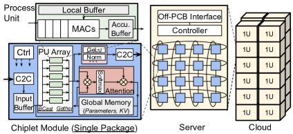
Combing the two solutions above, we propose a chiplet-based cloud-scale system design for LLM inference, called Chiplet Cloud. Our general Chiplet Cloud architecture is shown in Figure 6, which includes the high-level abstract architecture of different levels, from process unit (PU) to chiplet module,server,and cloud.
Starting from the bottom left, we start with the heart of Chiplet Cloud, a language model accelerator chiplet module that scales to data center inference. The module adopts a frequently-used PU-based architecture, with additional attention, nonlinear function, and normalization units. The Chiplet Cloud PU includes a local memory for holding parameters, multiple parallel MACs (multiply-accumulate) units, and an accumulation buffer. Model parameters and KVs are stored in a large on-chip global memory, as shown in Figure 6. No external memory like DRAM is required. The input buffer reads activation from another chiplet or the host through a chip-to-chip (C2C) router and broadcasts it to all PUs. Meanwhile, PUs load parameters into local memories. The PUs employ an output stationary dataflow pattern (Du et al., 2015) with spatial activation reuse and temporal partial sum accumulation reuse. This dataflow was selected as FC layers are the most compute intensive operation in the transformer decode layer which cannot exploit any weight reuse unless the batch size is greater than 1. The design maximizes parallelization and eliminates the need for inter-PU communication, reducing on-chip network overhead. The output of a PU either flows into the attention unit and then goes back to the PU array, or inputs into some nonlinear units like GeLu and normalization and is then sent outside the chip.
Figure 6 also shows one important feature of our design—a single chiplet module is a package, and multiple chiplets are connected through the board. Conventionally, chiplets are integrated into a single package via a package-level solution such as a silicon interposer (e.g., (Kannan et al., 2015)) or organic substrate (such as Simba (Shao et al., 2019) and AMD EPYC processor(Naffziger et al., 2021)) for better inter-chiplet communication. However, the package-level integration brings design challenges and overhead. Silicon interposers have a limited signal length. The organic substrate solution brings design challenges in package-level routing and power delivery (Naffziger et al., 2021). Instead, we use board-level chiplets in our Chiplet Cloud design according to the communication requirements. With an optimized workload partitioning and mapping strategy, we can reduce data traffic across chiplets. Chiplets have individual packages and are connected together via a 2D torus on-PCB network, which is able to accommodate the potentially different mapping strategies for different models and still reuse the same server. Compared to conventional package-level chiplet, the board-level chiplet architecture eliminates cost of advanced packaging.
Each Chiplet Cloud server contains a printed circuit board (PCB) with multiple chiplets, a controller and an off-PCB interface. The controller, which can be an FPGA or a microcontroller, dispatches remote procedure calls (RPCs) from off-PCB interface to all chiplets via the on-PCB 2D torus network. In the analysis of this paper, we model the use of ground-referenced signaling (GRS) links (Turner et al., 2018; Poulton et al., 2019) for inter-chiplet communication. Each chiplet module connects with adjacent chiplets over a full-duplex data link capable of 25 GB/s with up to 80 mm reach over the PCB. Other candidate chip-to-chip interfaces can be high-speed PCI-e, which has been widely used as interconnects for many deep learning chips (Smelyanskiy, 2019; Prabhakar and Jairath, 2021; Liu and Feng, 2021), or custom-designed links such as Google TPU’s Inter-Core Interconnect (Jouppi et al., 2020) and Graphcore’s IPU-links (Knowles, 2021). Off-PCB interfaces could be 10/100 Gigbit Ethernet or InfiniBand, enabling communication between adjacent servers.
3.4. Design Space Discussion
The Design space of our Chiplet Cloud includes multiple aspects from cross-stacks that affect the end-to-end performance. Some aspects include (1) Chiplet Module Size: small chips benefit from higher yields while incurring more per-chip overhead; (2) Per Chiplet Memory Size: more memory on chips means few chips required but few FLOPS per chip; (3) Silicon Per Server: more silicon per server reduces the communication between servers, but it is limited by the chiplet size, power and the cooling system; and (4) Software Mapping: the tradeoff between tensor model and pipeline model parallelism affects utilization and interconnect data communication. Since all of these aspects are highly coupled, a comprehensive design methodology is critical to optimize the end-to-end performance and TCO.
4. Design Methodology: Chiplet Cloud
A key challenge for optimizing the TCO of large scale-out systems is balancing the cost per operation and the watts per operation. To address this challenge, we propose a design methodology that can accurately explore the large design space of the Chiplet Cloud architectures and perform a cost-performance analysis of serving large generative language model. This design methodology, shown in Figure 7, is a two phase software-hardware co-design methodology: first a hardware exploration phase followed by a software evaluation phase. The methodology uses a brute-force exploration, with feasibility checks and pruning throughout to maintain a reasonable runtime performance.
This methodology is unlike traditional software-hardware co-design methodologies which typically start with extracting software characteristics and then derive hardware parameterizations based on preconceived assumptions about best practices. The design space for Chiplet Cloud is very large with many hardware parameterizations that need a careful balance to optimize for TCO/token. This makes traditional software-hardware co-design ineffective at finding truly optimal hardware design points. To avoid the need to bake-in these assumptions, our approach starts with a feasibility constrained design space exploration to generate every possible hardware design and then purge designs with power budgets, thermal outputs, or physical layouts that cannot be realized. Only then do we start evaluating hardware design points against specific generative LLMs to find a co-optimized Chiplet Cloud.
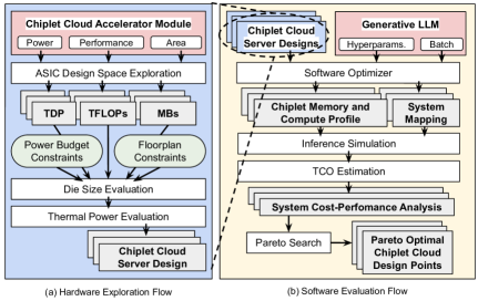
4.1. Phase 1: Hardware Exploration
The hardware exploration phase of the Chiplet Cloud design methodology (as shown in Figure 7(a)) is a bottom-up, LLM agnostic, design space exploration resulting in thousands of varying Chiplet Cloud server designs. The exploration starts with a flexible architectural description model of the Chiplet Cloud accelerator module described in more detail in section 3.3. This flexible architecture allows users to scale the on-chip memory capacity and the number of processing units within the constraints determined by microarchitectural limitations resulting in candidate architectures with varying peak power (TDP), peak performance (TFLOPs), and on-chip memory capacity (MBs).
Candidate architectures are then evaluated against a set of server level constraints including the max power budget and physical layout constraints. These constraints are based on the limitations of building a traditional 1U 19 inch rack mount server as found in ASIC Cloud (Magaki et al., 2016). The floorplan of the Chiplet Cloud server is derived from the optimal server floorplan found leveraging computation fluid dynamic simulations of airflow cooling of a 1U server. The floorplan is 8 lanes of silicon chips with physical ducting separating each lane to reduce turbulence.
Each candidate Chiplet Cloud accelerator is evaluated with these constraints to determine the best die size before undergoing thermal power analysis. Thermal analysis includes determining the total power dissipation per lane that can be achieved. A key factor to consider is the size of the chiplet die as this impacts the heatsink selection and thermal distribution throughout the server. Smaller chiplets allow for greater cooling efficiency within a lane by physically distributing the heat more evenly thus reducing hotspots.
The constraint analysis for Chiplet Cloud server designs as well as the overall TCO estimation that is performed during the second phase of the design methodology are heavily reliant on accurate power, area and performance estimation modeling of the accelerator module.
Area Estimation. The area estimation model for the Chiplet Cloud accelerator is derived from actual 7nm ASIC tapeouts found in the literature (Jouppi et al., 2021; Knowles, 2021), giving us a model for the and for the on-chip memory and PU array respectively. The silicon area is likely dominated by compute and memory device area. However, for a flexible accelerator architecture, auxiliary components of the chip can start to have a significant area overhead when the amount of memory and compute is small. Therefore, we also include the area overhead for the attention unit, activation unit, IO, on-chip networks, and control logic in the model.
Power Estimation. The power estimation model is also derived from the actual 7nm ASIC tapeout numbers found in the literature (Jouppi et al., 2021; Knowles, 2021). This gives us the TDP for running these 7nm ASICs at 100% utilization. We normalize this value to an W/FLOP at 100% utilization and use that value in combination with the parameterized compute power of the flexible architecture to determine a 100% utilization TDP estimation for our Chiplet Cloud accelerator. Combined with the area model, we limit the power density to be no more than , however during server design optimization we will further refine the peak power density limitations based on the full-server thermal analysis.
Performance Modeling. The performance model for the Chiplet Cloud accelerator used during hardware exploration is the peak-performance of the chiplet and is based on the number of PUs which is determined by the compute parameterization of the architecture. Every PU in the chiplet has a peak-performance of 2 operations per cycle (multiply-accumulate) and is estimated to run at 1GHz giving us 2 GFLOPs/s/PU. During the software evaluation phase of the design methodology, we will further refine the performance as a function of the software kernel, microarchitectural utilization and IO communication.
4.2. Phase 2: Software Evaluation
The second phase of the design methodology models the execution time of specific workloads across the hardware design points and searches for optimal Chiplet Cloud architectural configurations. The software evaluation flow is shown in Figure 7(b).
The first step is the software optimizer which takes the Chiplet Cloud server designs from phase 1 and a generative LLM workload and performs several optimizations including tensor parallelism and pipeline parallelism with microbatch tuning (Shoeybi et al., 2020; Narayanan et al., 2021). The optimizer will first look at the hyperparameters of the LLM, such as the model dimension , number of layers, context length, attention mechanism type (multi-head or multi-query), as well as expect batch size. Then it will decompose the full model into a collection of small kernels that can be mapped to the individual chiplets throughout the system. In cases where the model cannot fit into a single server, the server will be replicated to scale up the entire system until there are enough resources to execute the application. This results in a system mapping which has the portion of the model that each chiplet in the whole system will be responsible for executing, based on the chosen tensor and pipeline parallelism optimizations. There also exists a chiplet memory profile and chiplet compute profile for the portion of the model that will be running on the individual chiplet, which will allow us to accurately model the end-to-end performance of the full system. The memory profile contains information about the required memory for weights, activations, and the KV cache, while the compute profile contains the size and operations that the chiplet will need to perform including reduction operations caused by tensor parallelism optimizations.
The end-to-end performance model for the chiplet cloud system starts with understanding the compute latency inside each chiplet. This is based on the analytical analysis of the dataflow and compute latency of the mapped portion of the model as described by the compute profile. The compute profile defines which operations and the size of the operations that each chiplet will perform. We analyze the size and shape of these operations as they would be executed at the microarchitectural level to get a kernel compute latency and thus a kernel level utilization. This kernel level utilization is then used to scale the TDP of the chiplet to estimate the average kernel computational power.
Since the model has been split up across all of the chiplets, we must also model the data communication latency between the chiplets including all-reduce operations between collaborating chiplets that are working on operations that have been optimized with tensor parallelism. As mentioned in Section 3.3, each chiplet is equipped with a 25 GBps link to all the adjacent chiplets. However, the system mapping might have two chiplets that must communicate that exist on different servers. When this occurs, the performance of this link goes over a 10 Gbps Ethernet connection. This bandwidth reduction discourages many system mappings, particularly to those which all-reduce operations that must cross over server boundaries. These design points are generally removed during the Pareto optimization search given their large performance penalty.
Improved Software-Hardware Co-Design Model. The TCO model is a refined version of the model by Barroso et al (Barroso et al., 2013), which includes both capital expenditures (CapEx) and operating expenses (OpEx) from the system as well as the datacenter hosting the system. The CapEx for our server includes the silicon die cost, package cost, PCB cost, power supply unit cost, DC/DC converter costs, heatsink cost, fan costs, Ethernet controller cost, and control processor cost. The OpEx is calculated based on the power consumption of the system. Based on the system TDP and utilization, the full system average power consumption is used to determine the power draw from the silicon dies of the Chiplet Cloud accelerators. Additionally, the power cost due to inefficiencies of on-server DC/DC converts and the server power supply unit is also taken into consideration as is the power draw of the control processor, Ethernet controller and server fans.
To estimate the die cost, we first calculate the number of fully patterned dies per wafer (DPW). This is the number of rectangular dies with the given die size dimensions that we can slice out of a traditional circular wafer. Cost per die is then calculated as:
| (1) |
Where is wafer price, is testing cost, and is die yield. We use the classical negative binomial model for yield which is as follow:
| (2) |
Where is die area, is defect density and is cluster parameter. Since manufacturing yields drop with chip area, it makes economic sense to design smaller chips.
For each feasible server design that we found in the hardware exploration phase of the design methodology, we will profile the memory, compute and power for a given software optimization found from the original workload specification. With the memory profile, we can determine if we have enough storage for the software’s per-chip kernel with respect to the parameters, activation and KV cache size. If we do not have enough, then we consider this server configuration a non-feasible point to run this specific workload-software optimization combination. The number of servers is then selected to ensure that we have enough resources to fit the entire model given the per-chip memory profile. Additionally, compiling a network topography and assigning bandwidth numbers for all chiplet-to-chiplet communication links in the system depend on if the communication is on-server or inter-server. The network topography, multi-server architecture and chip computer profile are then all used to find the full end-to-end inference runtime of the workload. This performance along with the multi-server architecture and chip power profile are then fed into our TCO estimation engine where we can compute all TCO related metrics such as TCO/Token.
4.3. Generalizing the Design Methodology
While this work is focused on trying to find cloud-scale architectures with best-in-class TCO/Token performance, the methodology of designing scale-up cloud systems is still applicable to existing ASIC architectures or architectures designed for programmable devices such as CGRAs or FPGAs. Given an appropriate power, performance and area estimation model for the accelerator module, this methodology is applicable.
5. Case Studies
| Model | GPT-2 | T-NLG | GPT-3 | PaLM |
|---|---|---|---|---|
| 1600 | 4256 | 12288 | 18432 | |
| Layers | 48 | 78 | 96 | 118 |
| Attention Heads | 25 | 28 | 96 | 48 |
| Multi-query | No | No | No | Yes |
| # of Parameters | 1.4B | 17B | 175B | 540B |
| Context Length | 256, 2048, 8192 | |||
| Batch Size | 11024 | |||
| # of Design Points | 5,058,831 | 2,634,071 | 2,718,410 | 971,906 |
To evaluate our architecture and design methodology, we perform case studies of Chiplet Cloud on four language models at different scales, including GPT-2 (Radford et al., 2019) and GPT-3 (Brown et al., 2020) proposed by OpenAI, Turing NLG (T-NLG) (Microsoft, 2020) proposed by Microsoft and NVIDIA, and PaLM (Chowdhery et al., 2022) proposed by Google. Dimensions of these models are shown in Table 1. Note that PaLM uses multiquery attention, where key and value are shared across the attention heads, which reduces the size of the KV cache by a factor of number of heads. All Chiplet Cloud chip designs utilize TSMC 7nm technology in this paper.
5.1. Design Space Exploration
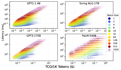
We did a thorough design exploration on each model. For each one, we explored 3 different context length scenarios: 256, 2048 and 8192. Normally, the longer the context length, the better the model performance, but it requires more memory and more computation. For the analysis below, the context length is 2048 if not explicitly mentioned. We also explore the input batch sizes from 1 to 1024. In total we generate over 10M valid design points. Each design point combines the result from both hardware exploration and software evaluation, which includes hardware design (chip and server), software mapping (tensor parallelism size, pipeline parallelism size, batch size and micro-batch size), cost (power, CapEx and TCO) and performance (latency and throughput), etc. Figure 8 shows all valid design points for 4 models. The color indicates the batch size.
The rich information from design space exploration helps designers find the most suitable design given any type of constraint and any optimization goal. In Table 2, we show the latency and TCO/Token optimal designs for four models. Each design is optimized just for the model. Latency-optimal designs are always preferred when the batch size is 1, since it requires fewer operations. These designs also tend to use large chips with higher TOPS to minimize inter-node communication and computation latency. At the same time, the TCO per token of these designs is high, which mainly depends on utilization. It is well known that LLMs have low hardware utilization when the batch size is small. For the TCO-optimal designs, the batch size are much larger (64 to 128). Large batch size is good for utilization while requiring larger KV cache and thus more silicon. This means we either need bigger chips which greatly increase CapEx, or more chips which generate more inter-node traffic and hurt throughput. An appropriate batch size to balance each factor is essential to achieve good TCO/Token, but can be difficult to find. The 8 optimal design points all have different chip, server designs, and different mapping strategies, demonstrating the importance of our design methodology—every aspect of the system affects performance and cost, and different workloads require different optimizations.
| Optimization Target (per Token) | Latency | TCO | Latency | TCO | Latency | TCO | Latency | TCO |
| Die Size (mm2) | 800 | 620 | 800 | 160 | 600 | 160 | 800 | 260 |
| MB per Chip | 1110 | 831 | 1170 | 210 | 884 | 216 | 1170 | 364 |
| TOPS per Chip | 140 | 143 | 46 | 17 | 13.8 | 8.6 | 46 | 14.5 |
| Chips per Server | 8 | 8 | 32 | 80 | 80 | 144 | 32 | 96 |
| Number of Servers | 1 | 2 | 1 | 8 | 6 | 32 | 30 | 30 |
| Tensor Parallelism Size | 2 | 1 | 32 | 16 | 80 | 48 | 16 | 24 |
| Pipeline Parallelism Size | 2 | 16 | 1 | 39 | 6 | 96 | 59 | 118 |
| Batch Size | 1 | 16 | 1 | 32 | 1 | 64 | 1 | 128 |
| Micro-Batch Size | 1 | 1 | 1 | 1 | 1 | 1 | 1 | 1 |
| Latency (ms) | 0.018 | 0.025 | 0.133 | 0.28 | 0.81 | 1.89 | 2.86 | 4.8 |
| Cents/1K Tokens | 0.0002 | 0.00005 | 0.004 | 0.001 | 0.185 | 0.018 | 2.28 | 0.031 |
| Model | GPT-2 | Turing NLG | GPT-3 | PaLM 540B | ||||
5.2. Design Insights
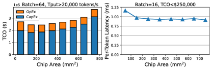
We first study how chip size affects TCO and performance. Figure 9 shows the results of GPT-3 in two different scenarios. On the left is how we should choose die size to lower TCO for a given minimum throughput requirement. Compared to chips over 700mm2, which is the size of many traditional large monolithic chips, a chip around 200 mm2 reduces TCO by about 1.5 and still meets the throughput constraint. We can also find the CapEX exceeds 80% of TCO for most designs. Figure on the right shows what are the best latency for chips of different sizes given the TCO budget. Except for the smallest size chip, others all achieve similar latencies. This shows that proper chip size can effectively reduce TCO without compromising performance.
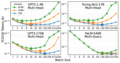
We further investigate how the batch size affects TCO/Token. Figure 10 shows the results on 4 different models and 3 different context length. When the batch size is increased from 1, the TCO/Tokens become better because the compute unit utilization increases. Larger batch sizes also provide more opportunities to exploit pipeline parallelism to improve overall system utilization. As the batch size continues to increase, the utilization will reach a peak. For the traditional multi-head model, more silicon is required for KV cache in large batch size and long contexts, which significantly increases TCO/Token. Chiplet Cloud supports batch sizes up to 64 with near-optimal TCO/Token for these models. For multi-query model PaLM, Chiplet Cloud supports batch sizes up to 1024 with near-optimal TCO/Token. The cost of longer contexts is negligible, especially when the batch size is not too large.
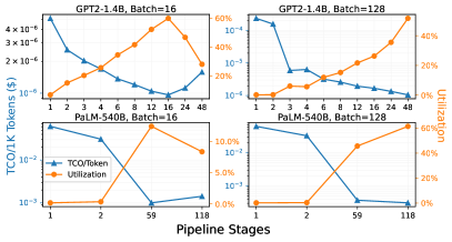
Lastly, we study how the mapping strategy affects TCO/Token for a given batch size. As shown in Figure 11, when the number of pipeline stages (i.e. the pipeline parallelism size) is close to the batch size, the system utilization is the largest and the TCO/Token is optimal. When these two numbers are similar, the system can take full advantage of pipeline parallelism with a micro-batch size of 1, so the number of micro-batches is also close (if not equal) to the pipeline stage (Aminabadi et al., 2022). This helps balance the latency of micro-batches passing through all pipeline stages and pipeline stages completing all micro-batches.
6. Evaluation
In this section, we evaluate the performance and cost of Chiplet Cloud for serving large language models. The key metric we are targeting is TCO/Token. TCO/Token is measured as cost per token generated and is the key factor in the ability to democratize of LLMs. One of the most popular business models for generative LLMs is also to charge users per generated token. Lower TCO/Token not only adds more profit margins, but also makes LLMs more approachable. We compare Chiplet Cloud to state-of-the-art GPU and TPU cloud implementations. We also demonstrate the benefits of our architectural design choices and evaluate the flexibility of Chiplet Cloud architectures.
6.1. Comparison with GPUs and TPUs
In Table 3, we compare Chiplet Cloud versus state-of-the-art GPU (Aminabadi et al., 2022) and TPU (Pope et al., 2022) implementations. Neither work is specifically optimized for TCO/Token. For our comparison, we choose the throughput optimal result for GPU, and the utilization optimal result for TPU, which are key indicators that you are close to TCO/Token optimal. TCO for GPUs and TPUs are based on the best cloud rental price we could find (Cloud, 2023; Lambda, 2023). Compared to A100 GPU and TPUv4 clouds, Chiplet Cloud achieves and improvement on TCO/Token, respectively.
6.2. Design Choice Sanity Check
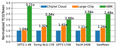
To demonstrate the benefits of our design choices, including fitting all parameters in on-chip SRAM and using many smaller chiplet accelerators, we compare Chiplet Cloud with two baseline systems. The first system (HBM) is a conventional HBM-based accelerator system. We assume each chip has a 8GB HBM die that supports up to 900GB/s bandwidth. All model parameters and KV cache are on HBM. The second system (Large Chip) is Chiplet Cloud without chip size moderation. Like a traditional large monolithic chip, it tries to put as much memory and as many processing units as possible on the chip. We pass the hardware specs of both systems to our design methodology and search for the optimal mapping strategies. Figure 12 shows the optimal TCO/Token of both systems on 4 models. All numbers are normalized to Chiplet Cloud. On average, Chiplet Cloud outperforms the Large Chip system by 2.49 TCO/TOken and the HBM system by 1.24 TCO/Token.
| Models | GPT-3 | PaLM 540B | ||||||||||||
|---|---|---|---|---|---|---|---|---|---|---|---|---|---|---|
|
|
|
|
|
||||||||||
| TCO/sec (cents) | 0.61 | 7.82 | 0.83 | 2.61 | ||||||||||
| Latency (ms) | 1.9 | 620.0 | 4.8 | 93.8 | ||||||||||
| Tokens/sec | 33,791 | 4,608 | 26,667 | 5,461 | ||||||||||
|
0.018 | 1.698 | 0.031 | 0.478 | ||||||||||
| Improvement | 94 | 15 | ||||||||||||
6.3. Generic Chiplet Cloud Servers
Up until now, we have only shown Chiplet Cloud optimized for a single workload (one language model with fixed context length). However, the separation of hardware exploration and software evaluation in our design methodology makes it possible to find suitable server designs for multiple workloads simultaneously, thus increasing the flexibility of the resulting Chiplet Cloud. This is done by applying a performance-cost analysis of each Chiplet Cloud server design across multiple workloads simultaneously to find design points that are in aggregate TCO/Token optimal.
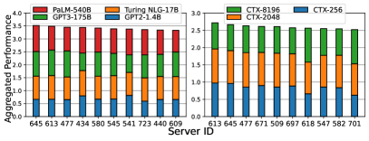
During hardware exploration, we generate 1073 valid unique server designs. In Figure 13, we list the top 10 servers that achieve the best aggregated performance (TCO/Token) on different models (left), and on the same model but with different context lengths (right). The performance shown of the server across all workloads is normalized to the aggregated performance achieved by the optimal server for each individual workload. If a server achieves the optimal performance on all 4 workloads, it would have an aggregated performance of 4.0. Compared to the aggregated performance of the individually optimized servers, the best single server TCO/Token across the 4 LLMs only dropped 12% while the best single server TCO/Token across the 3 context lengths only dropped 9%.
7. Related Work
Training and serving large language models on GPU and TPU has attracted a lot of attention in recent years. Megatron-LM (Shoeybi et al., 2020) proposes a tensor partitioning strategy that reduces the inter-node communication. (Narayanan et al., 2021) improves pipeline parallelism and combines it with Megatron-LM and achieves high aggregate throughput. DeepSpeed (Rajbhandari et al., 2022; Aminabadi et al., 2022) proposes multi-GPU training and inference solution to minimize latency while maximizing throughput. PaLM (Chowdhery et al., 2022) train a 540B parameter model on 6144 TPUv4 chips using Pathways (Barham et al., 2022). (Pope et al., 2022) develops an analytical model to select the mapping strategy optimized for inference on TPUv4.
Many ASIC accelerators for transformer NNs have been proposed. SpAtten (Wang et al., 2021) exploits the token and head sparsity and quantization opportunities in the attention block. ELSA (Ham et al., 2021) presents an approximation scheme for the attention mechanism. EdgeBERT (Tambe et al., 2021) leverages dynamic voltage-frequency scaling based on early exit prediction of ALBERT (Lan et al., 2020). (Wang et al., 2022) designs a transformer accelerator in 28nm using approximate-computing and sparsity speculation. These designs focus on optimizing the attention block, which is usually not the bottleneck for LLMs.
To exploit chiplet technology on deep learning accelerators, Simba (Shao et al., 2019; Venkatesan et al., 2019) implements the first 36-chiplet prototype multi-chip-modules (MCM) system for deep learning inference. COMB-MCM (Zhu et al., 2022) uses chiplets to improve the scalability of their computing-on-memory-boundary NN processors. NN-Baton (Tan et al., 2021) proposes a framework to explore the chiplet design space for convolutional NN. These works focus on small-scale optimizations—chiplets in a single package, and do not demonstrate scalability to support LLM.
8. Conclusion
This paper presents Chiplet Cloud, a chiplet-based ASIC AI supercomputer architecture that achieves unprecedented TCO/Token for serving large generative language model. Chiplet Cloud fits all model parameters inside the on-chip SRAMs to eliminate bandwidth limitations while moderating the die size to improve system costs while leveraging software mappings to overcome data communication overhead. We propose a comprehensive design methodology that accurately explores a spectrum of major design trade-offs in the joint space of hardware-software and generates a detailed performance-cost analysis on all valid design points. With this methodology, we design Chiplet Cloud systems for four language models of different sizes and achieved and better TCO/Token compared to A100 GPU and TPUv4, respectively. We believe Chiplet Cloud to be the best solution to democratise modern and future large generative language models.
Acknowledgements
This work was supported by NSF Award 2118628.
References
- (1)
- Aminabadi et al. (2022) Reza Yazdani Aminabadi, Samyam Rajbhandari, Ammar Ahmad Awan, Cheng Li, Du Li, Elton Zheng, Olatunji Ruwase, Shaden Smith, Minjia Zhang, Jeff Rasley, and Yuxiong He. 2022. DeepSpeed- Inference: Enabling Efficient Inference of Transformer Models at Unprecedented Scale. In SC22: International Conference for High Performance Computing, Networking, Storage and Analysis. IEEE, Dallas, TX, USA, 1–15. https://doi.org/10.1109/SC41404.2022.00051
- Barham et al. (2022) Paul Barham, Aakanksha Chowdhery, Jeff Dean, Sanjay Ghemawat, Steven Hand, Dan Hurt, Michael Isard, Hyeontaek Lim, Ruoming Pang, Sudip Roy, Brennan Saeta, Parker Schuh, Ryan Sepassi, Laurent El Shafey, Chandramohan A. Thekkath, and Yonghui Wu. 2022. Pathways: Asynchronous Distributed Dataflow for ML. arXiv:2203.12533 [cs] (March 2022). http://arxiv.org/abs/2203.12533 arXiv: 2203.12533.
- Barroso et al. (2013) Luiz André Barroso, Urs Hölzle, and Parthasarathy Ranganathan. 2013. The Datacenter as a Computer: Designing Warehouse-Scale Machines. Synthesis lectures on computer architecture (2013), 209.
- Brown et al. (2020) Tom B. Brown, Benjamin Mann, Nick Ryder, Melanie Subbiah, Jared Kaplan, Prafulla Dhariwal, Arvind Neelakantan, Pranav Shyam, Girish Sastry, Amanda Askell, Sandhini Agarwal, Ariel Herbert-Voss, Gretchen Krueger, Tom Henighan, Rewon Child, Aditya Ramesh, Daniel M. Ziegler, Jeffrey Wu, Clemens Winter, Christopher Hesse, Mark Chen, Eric Sigler, Mateusz Litwin, Scott Gray, Benjamin Chess, Jack Clark, Christopher Berner, Sam McCandlish, Alec Radford, Ilya Sutskever, and Dario Amodei. 2020. Language Models are Few-Shot Learners. arXiv:2005.14165 [cs] (July 2020). http://arxiv.org/abs/2005.14165 arXiv: 2005.14165.
- Chowdhery et al. (2022) Aakanksha Chowdhery, Sharan Narang, Jacob Devlin, Maarten Bosma, Gaurav Mishra, Adam Roberts, Paul Barham, Hyung Won Chung, Charles Sutton, Sebastian Gehrmann, Parker Schuh, Kensen Shi, Sasha Tsvyashchenko, Joshua Maynez, Abhishek Rao, Parker Barnes, Yi Tay, Noam Shazeer, Vinodkumar Prabhakaran, Emily Reif, Nan Du, Ben Hutchinson, Reiner Pope, James Bradbury, Jacob Austin, Michael Isard, Guy Gur-Ari, Pengcheng Yin, Toju Duke, Anselm Levskaya, Sanjay Ghemawat, Sunipa Dev, Henryk Michalewski, Xavier Garcia, Vedant Misra, Kevin Robinson, Liam Fedus, Denny Zhou, Daphne Ippolito, David Luan, Hyeontaek Lim, Barret Zoph, Alexander Spiridonov, Ryan Sepassi, David Dohan, Shivani Agrawal, Mark Omernick, Andrew M. Dai, Thanumalayan Sankaranarayana Pillai, Marie Pellat, Aitor Lewkowycz, Erica Moreira, Rewon Child, Oleksandr Polozov, Katherine Lee, Zongwei Zhou, Xuezhi Wang, Brennan Saeta, Mark Diaz, Orhan Firat, Michele Catasta, Jason Wei, Kathy Meier-Hellstern, Douglas Eck, Jeff Dean, Slav Petrov, and Noah Fiedel. 2022. PaLM: Scaling Language Modeling with Pathways. arXiv:2204.02311 [cs] (April 2022). http://arxiv.org/abs/2204.02311 arXiv: 2204.02311.
- Cloud (2023) Google Cloud. 2023. Cloud TPU pricing. https://cloud.google.com/tpu/pricing##v4-pricing
- Du et al. (2015) Zidong Du, Robert Fasthuber, Tianshi Chen, Paolo Ienne, Ling Li, Tao Luo, Xiaobing Feng, Yunji Chen, and Olivier Temam. 2015. ShiDianNao: Shifting Vision Processing Closer to the Sensor. SIGARCH Comput. Archit. News 43, 3S (jun 2015), 92–104. https://doi.org/10.1145/2872887.2750389
- Fowers et al. (2018) Jeremy Fowers, Kalin Ovtcharov, Michael Papamichael, Todd Massengill, Ming Liu, Daniel Lo, Shlomi Alkalay, Michael Haselman, Logan Adams, Mahdi Ghandi, Stephen Heil, Prerak Patel, Adam Sapek, Gabriel Weisz, Lisa Woods, Sitaram Lanka, Steven K. Reinhardt, Adrian M. Caulfield, Eric S. Chung, and Doug Burger. 2018. A Configurable Cloud-Scale DNN Processor for Real-Time AI. In ISCA. Los Angeles, CA, 1–14. https://doi.org/10.1109/ISCA.2018.00012
- GitHub (2023) GitHub. 2023. GitHub Copilot Your AI pair programmer. https://github.com/features/copilot
- Ham et al. (2021) Tae Jun Ham, Yejin Lee, Seong Hoon Seo, Soosung Kim, Hyunji Choi, Sung Jun Jung, and Jae W. Lee. 2021. ELSA: Hardware-Software Co-design for Efficient, Lightweight Self-Attention Mechanism in Neural Networks. In ISCA. IEEE, Valencia, Spain, 692–705. https://doi.org/10.1109/ISCA52012.2021.00060
- Jouppi et al. (2021) Norman P. Jouppi, Doe Hyun Yoon, Matthew Ashcraft, Mark Gottscho, Thomas B. Jablin, George Kurian, James Laudon, Sheng Li, Peter Ma, Xiaoyu Ma, Thomas Norrie, Nishant Patil, Sushma Prasad, Cliff Young, Zongwei Zhou, and David Patterson. 2021. Ten Lessons From Three Generations Shaped Google’s TPUv4i : Industrial Product. In ISCA. 1–14. https://doi.org/10.1109/ISCA52012.2021.00010
- Jouppi et al. (2020) Norman P. Jouppi, Doe Hyun Yoon, George Kurian, Sheng Li, Nishant Patil, James Laudon, Cliff Young, and David Patterson. 2020. A domain-specific supercomputer for training deep neural networks. Commun. ACM 63, 7 (June 2020), 67–78. https://doi.org/10.1145/3360307
- Kannan et al. (2015) Ajaykumar Kannan, Natalie Enright Jerger, and Gabriel H. Loh. 2015. Enabling interposer-based disintegration of multi-core processors. In MICRO. 546–558. https://doi.org/10.1145/2830772.2830808 ISSN: 2379-3155.
- Khazraee et al. (2017) Moein Khazraee, Lu Zhang, Luis Vega, and Michael Bedford Taylor. 2017. Moonwalk: NRE Optimization in ASIC Clouds. In ASPLOS. ACM, Xi’an China, 511–526. https://doi.org/10.1145/3037697.3037749
- Knowles (2021) Simon Knowles. 2021. Graphcore Colossus Mk2 IPU. In Hot Chips.
- Lambda (2023) Lambda. 2023. The best prices for cloud GPUs. https://lambdalabs.com/service/gpu-cloud
- Lan et al. (2020) Zhenzhong Lan, Mingda Chen, Sebastian Goodman, Kevin Gimpel, Piyush Sharma, and Radu Soricut. 2020. ALBERT: A Lite BERT for Self-supervised Learning of Language Representations. arXiv:1909.11942 [cs] (Feb. 2020). http://arxiv.org/abs/1909.11942 arXiv: 1909.11942.
- Liu and Feng (2021) Ryan Liu and Chuang Feng. 2021. AI Compute Chip from Enflame. In Hot Chips. 1–27. https://doi.org/10.1109/HCS52781.2021.9567224 ISSN: 2573-2048.
- Magaki et al. (2016) Ikuo Magaki, Moein Khazraee, Luis Vega Gutierrez, and Michael Bedford Taylor. 2016. ASIC Clouds: Specializing the Datacenter. In ISCA. IEEE, Seoul, South Korea, 178–190. https://doi.org/10.1109/ISCA.2016.25
- Microsoft (2020) Microsoft. 2020. Turing-NLG: A 17-billion-parameter language model by Microsoft. https://www.microsoft.com/en-us/research/blog/turing-nlg-a-17-billion-parameter-language-model-by-microsoft/
- Mohsin (2023) Maryam Mohsin. 2023. 10 Google Search Statistics You Need to Know in 2023. https://www.oberlo.com/blog/google-search-statistics#:~:text=We%20know%20that%20there%20are,Internet%20Live%20Stats%2C%202022).
- Naffziger et al. (2021) Samuel Naffziger, Noah Beck, Thomas Burd, Kevin Lepak, Gabriel H. Loh, Mahesh Subramony, and Sean White. 2021. Pioneering Chiplet Technology and Design for the AMD EPYC™ and Ryzen™ Processor Families : Industrial Product. In ISCA. IEEE, Valencia, Spain, 57–70. https://doi.org/10.1109/ISCA52012.2021.00014
- Narayanan et al. (2021) Deepak Narayanan, Mohammad Shoeybi, Jared Casper, Patrick LeGresley, Mostofa Patwary, Vijay Korthikanti, Dmitri Vainbrand, Prethvi Kashinkunti, Julie Bernauer, Bryan Catanzaro, Amar Phanishayee, and Matei Zaharia. 2021. Efficient large-scale language model training on GPU clusters using megatron-LM. In SC. ACM, St. Louis Missouri, 1–15. https://doi.org/10.1145/3458817.3476209
- OpenAI (2022) OpenAI. 2022. Introducing ChatGPT. https://openai.com/blog/chatgpt
- Pope et al. (2022) Reiner Pope, Sholto Douglas, Aakanksha Chowdhery, Jacob Devlin, James Bradbury, Anselm Levskaya, Jonathan Heek, Kefan Xiao, Shivani Agrawal, and Jeff Dean. 2022. Efficiently Scaling Transformer Inference. http://arxiv.org/abs/2211.05102 arXiv:2211.05102 [cs].
- Poulton et al. (2019) John W. Poulton, John M. Wilson, Walker J. Turner, Brian Zimmer, Xi Chen, Sudhir S. Kudva, Sanquan Song, Stephen G. Tell, Nikola Nedovic, Wenxu Zhao, Sunil R. Sudhakaran, C. Thomas Gray, and William J. Dally. 2019. A 1.17-pJ/b, 25-Gb/s/pin Ground-Referenced Single-Ended Serial Link for Off- and On-Package Communication Using a Process- and Temperature-Adaptive Voltage Regulator. IEEE Journal of Solid-State Circuits 54, 1 (Jan. 2019), 43–54. https://doi.org/10.1109/JSSC.2018.2875092 Conference Name: IEEE Journal of Solid-State Circuits.
- Prabhakar and Jairath (2021) Raghu Prabhakar and Sumti Jairath. 2021. SambaNova SN10 RDU:Accelerating Software 2.0 with Dataflow. In Hot Chips. 1–37. https://doi.org/10.1109/HCS52781.2021.9567250 ISSN: 2573-2048.
- Radford et al. (2019) Alec Radford, Jeffrey Wu, Rewon Child, David Luan, Dario Amodei, and Ilya Sutskever. 2019. Language Models are Unsupervised Multitask Learners. (2019), 24.
- Rajbhandari et al. (2022) Samyam Rajbhandari, Conglong Li, Zhewei Yao, Minjia Zhang, Reza Yazdani Aminabadi, Ammar Ahmad Awan, Jeff Rasley, and Yuxiong He. 2022. DeepSpeed-MoE: Advancing Mixture-of-Experts Inference and Training to Power Next-Generation AI Scale. http://arxiv.org/abs/2201.05596 arXiv:2201.05596 [cs].
- Shao et al. (2019) Yakun Sophia Shao, Jason Clemons, Rangharajan Venkatesan, Brian Zimmer, Matthew Fojtik, Nan Jiang, Ben Keller, Alicia Klinefelter, Nathaniel Pinckney, Priyanka Raina, Stephen G. Tell, Yanqing Zhang, William J. Dally, Joel Emer, C. Thomas Gray, Brucek Khailany, and Stephen W. Keckler. 2019. Simba: Scaling Deep-Learning Inference with Multi-Chip-Module-Based Architecture. In MICRO. ACM, Columbus OH USA, 14–27. https://doi.org/10.1145/3352460.3358302
- Shoeybi et al. (2020) Mohammad Shoeybi, Mostofa Patwary, Raul Puri, Patrick LeGresley, Jared Casper, and Bryan Catanzaro. 2020. Megatron-LM: Training Multi-Billion Parameter Language Models Using Model Parallelism. arXiv:1909.08053 [cs] (March 2020). http://arxiv.org/abs/1909.08053 arXiv: 1909.08053.
- Smelyanskiy (2019) Misha Smelyanskiy. 2019. Zion: Facebook Next- Generation Large Memory Training Platform. In Hot Chips. 1–22. https://doi.org/10.1109/HOTCHIPS.2019.8875650 ISSN: 2573-2048.
- Systems (2019) Cerebras Systems. 2019. Wafer-Scale Deep Learning. In Hot Chips. https://www.hotchips.org/hc31/HC31_1.13_Cerebras.SeanLie.v02.pdf
- Tambe et al. (2021) Thierry Tambe, Coleman Hooper, Lillian Pentecost, Tianyu Jia, En-Yu Yang, Marco Donato, Victor Sanh, Paul Whatmough, Alexander M. Rush, David Brooks, and Gu-Yeon Wei. 2021. EdgeBERT: Sentence-Level Energy Optimizations for Latency-Aware Multi-Task NLP Inference. In MICRO. ACM, Virtual Event Greece, 830–844. https://doi.org/10.1145/3466752.3480095
- Tan et al. (2021) Zhanhong Tan, Hongyu Cai, Runpei Dong, and Kaisheng Ma. 2021. NN-Baton: DNN Workload Orchestration and Chiplet Granularity Exploration for Multichip Accelerators. In ISCA. 1013–1026. https://doi.org/10.1109/ISCA52012.2021.00083 ISSN: 2575-713X.
- Turner et al. (2018) Walker J. Turner, John W. Poulton, John M. Wilson, Xi Chen, Stephen G. Tell, Matthew Fojtik, Thomas H. Greer, Brian Zimmer, Sanquan Song, Nikola Nedovic, Sudhir S. Kudva, Sunil R. Sudhakaran, Rizwan Bashirullah, Wenxu Zhao, William J. Dally, and C. Thomas Gray. 2018. Ground-referenced signaling for intra-chip and short-reach chip-to-chip interconnects. In 2018 IEEE Custom Integrated Circuits Conference (CICC). 1–8. https://doi.org/10.1109/CICC.2018.8357077 ISSN: 2152-3630.
- Vaswani et al. (2017) Ashish Vaswani, Noam Shazeer, Niki Parmar, Jakob Uszkoreit, Llion Jones, Aidan N. Gomez, Lukasz Kaiser, and Illia Polosukhin. 2017. Attention Is All You Need. arXiv:1706.03762 [cs] (Dec. 2017). http://arxiv.org/abs/1706.03762 arXiv: 1706.03762.
- Venkatesan et al. (2019) Rangharajan Venkatesan, Yakun Sophia Shao, Brian Zimmer, Jason Clemons, Matthew Fojtik, Nan Jiang, Ben Keller, Alicia Klinefelter, Nathaniel Pinckney, Priyanka Raina, Stephen G. Tell, Yanqing Zhang, William J. Dally, Joel S. Emer, C. Thomas Gray, Stephen W. Keckler, and Brucek Khailany. 2019. A 0.11 pJ/Op, 0.32-128 Tops, Scalable Multi-Chip-Module-Based Deep Neural Network Accelerator Designed with A High-Productivity VLSI Methodology. In Hot Chips. 1–24. https://doi.org/10.1109/HOTCHIPS.2019.8875657 ISSN: 2573-2048.
- Wang et al. (2021) Hanrui Wang, Zhekai Zhang, and Song Han. 2021. SpAtten: Efficient Sparse Attention Architecture with Cascade Token and Head Pruning. arXiv:2012.09852 [cs] (Jan. 2021). http://arxiv.org/abs/2012.09852 arXiv: 2012.09852.
- Wang et al. (2022) Yang Wang, Yubin Qin, Dazheng Deng, Jingchuan Wei, Yang Zhou, Yuanqi Fan, Tianbao Chen, Hao Sun, Leibo Liu, Shaojun Wei, and Shouyi Yin. 2022. A 28nm 27.5TOPS/W Approximate-Computing-Based Transformer Processor with Asymptotic Sparsity Speculating and Out-of-Order Computing. In ISSCC, Vol. 65. 1–3. https://doi.org/10.1109/ISSCC42614.2022.9731686 ISSN: 2376-8606.
- Zhu et al. (2022) Haozhe Zhu, Bo Jiao, Jinshan Zhang, Xinru Jia, Yunzhengmao Wang, Tianchan Guan, Shengcheng Wang, Dimin Niu, Hongzhong Zheng, Chixiao Chen, Mingyu Wang, Lihua Zhang, Xiaoyang Zeng, Qi Liu, Yuan Xie, and Ming Liu. 2022. COMB-MCM: Computing-on-Memory-Boundary NN Processor with Bipolar Bitwise Sparsity Optimization for Scalable Multi-Chiplet-Module Edge Machine Learning. In ISSCC, Vol. 65. 1–3. https://doi.org/10.1109/ISSCC42614.2022.9731657 ISSN: 2376-8606.