High-Strength Amorphous Silicon Carbide for Nanomechanics
Abstract
For decades, mechanical resonators with high sensitivity have been realized using thin-film materials under high tensile loads. Although there have been remarkable strides in achieving low-dissipation mechanical sensors by utilizing high tensile stress, the performance of even the best strategy is limited by the tensile fracture strength of the resonator materials. In this study, a wafer-scale amorphous thin film is uncovered, which has the highest ultimate tensile strength ever measured for a nanostructured amorphous material. This silicon carbide (SiC) material exhibits an ultimate tensile strength of over 10 GPa, reaching the regime reserved for strong crystalline materials and approaching levels experimentally shown in graphene nanoribbons. Amorphous SiC strings with high aspect ratios are fabricated, with mechanical modes exceeding quality factors at room temperature, the highest value achieved among SiC resonators. These performances are demonstrated faithfully after characterizing the mechanical properties of the thin film using the resonance behaviors of free-standing resonators. This robust thin-film material has significant potential for applications in nanomechanical sensors, solar cells, biological applications, space exploration and other areas requiring strength and stability in dynamic environments. The findings of this study open up new possibilities for the use of amorphous thin-film materials in high-performance applications.
I Introduction
Advances in nanotechnology have revolutionized a broad spectrum of fields, with the development of tensile-loaded, thin-film mechanical devices playing a pivotal role in state-of-the-art force, acceleration, and displacement sensing [1, 2, 3, 4, 5, 6, 7]. Two approaches are used to boost the sensitivity of nanomechanical resonators under tensile loads. One approach fabricates the resonators using different thin-film materials in pursuit of films with low mechanical loss tangents resulting in higher intrinsic mechanical quality factors. In room temperature environments, high-tensile amorphous silicon nitride (a-Si3N4) nanomechanical resonators have marked some of the best performing devices in ultra-sensitive mechanical detectors [8, 9, 10, 11, 12, 13]. Despite the fact that crystalline thin film materials (e.g. crystalline silicon (c-Si) [14], crystalline silicon carbide (c-SiC) [15, 16]) and graphene are expected to have higher theoretical limits, their projected performance relies on having perfect crystal structures with no defects (e.g. edge defects). Additionally it is difficult to practically attain crystalline thin-films [15, 14] which can be easily deposited, have good film isotropy [17] and few lattice imperfections [15, 14]. By nanostructuring edges into free-standing crystalline devices, one introduces a form of defect by exposing the edge of the crystal where fracture can initiate under high-tensile loads [18, 19, 20].
The other approach to attain state-of-the-art sensors is by innovating designs of the nanomechanical resonators’ geometries to have high stresses at crucial regions of the resonator when it vibrates. Ultimately the design space of these resonators is constrained by the thin film materials’ tensile fracture limits or ultimate tensile strength (UTS). The UTS of a thin-film is fundamentally lower after being nanostructured into a suspended geometry with edges, since the introduced crystalline defects such as dislocations can facilitate the propagation of cracks [21, 22]. For example, the UTS of a-Si3N4 thin film has been shown to be 6.8 GPa [23]. To date, only crystalline and 2D materials have experimentally demonstrated UTS surpassing 10 GPa after being top-down nanofabricated [24, 25, 26, 19]. Among 2D crystalline materials, graphene harbors one of the highest theoretical UTS [27, 26], but practically reaching the limit is also challenging due to lattice imperfections [28], atomically irregular edges [19], or sparser grain boundaries [29] resulting from nanostructuring processes, which lead to a reduced fracture limit when it is tensile-loaded. In this regard, amorphous thin films with high UTS offer more design freedom for free-standing nanostructures, due to their lack of both crystalline defects and sensitivity to notches [30, 31, 32, 33]. Apart from allowing the enhancement of the Q factor of nanomechanical resonators, higher material UTS can enable the devices to perform better in diverse and harsh environments.
Among the materials processing the highest ultimate tensile strengths [24, 34, 35], silicon carbide (SiC) is attracting rising interest and demand both in industry and in academia in recent years due to its exceptional mechanical, chemical, electrical and optical properties [36, 37, 38, 39, 40, 41, 42]. SiC exists in three forms: single crystalline, poly-crystalline, and amorphous, all of which can be fabricated into thin films for various applications [36]. Among them, amorphous SiC (a-SiC) thin film offers distinct advantages over their crystalline counterparts [43, 44, 45, 46, 47, 48, 19, 25], including lower deposition temperature, compatibility with various substrates, isotropic physical properties, and the ability to deposit on large wafer scales. The widespread applications of a-SiC range from protective coatings to avoid mechanical wear [49] and chemical corrosion [50, 51], low-loss deposited dielectrics [52], device and functional layers for solar cells [53, 54, 55], MEMS sensors [56, 57, 58, 44] and electron transparent windows [43], low-loss optical resonators [59] and integrated photonics [60, 61], bio-molecular [62] and medical [63] applications, as well as gratings with nano-pillars [64, 65], to name a few. The versatility of a-SiC makes it a promising material for the high-yield production of integrated mechanical, electronic and photonic devices on a chip, paving the way for applications in sensing [6, 66], transduction [67], and quantum technology [68, 69].
In this work, we demonstrate wafer-scale amorphous films that harbor an ultimate tensile strength over 10 GPa after nanostructuring, a regime that is conventionally reserved for ultra-strong crystalline and 2D materials. Using delicate nanofabrication techniques, we produce several different nanomechanical resonators that can accurately determine the mechanical properties of SiC thin films such as density, Young’s modulus, Poisson ratio, and ultimate tensile strength. Notably, our highest measured tensile strength (10 GPa) is comparable to the values shown for c-SiC [24] and approaching the experimental values obtained for double-clamped graphene nano-ribbon [19]. We achieve mechanical quality factor up to with a-SiC mechanical resonators, and measure loss-tangents on par with other materials used in high-precision sensors. Beyond sensing, these strong films open up new possibilities in high-performance nanotechnology, including thin solar cell technologies [53], mechanical sensing [70], biological technologies[71] and even lightsail space exploration [72].
II Fabrication of amorphous SiC resonators
In pursuit of thin film materials for nanomechanical resonators with low mechanical dissipation, high film quality and high tensile stress are desirable. The Low Pressure Chemical Vapor Deposition (LPCVD) technique is preferred for these requirements, since its low pressure and high temperature deposition environment ensures lower defect density and higher thermal stress. The non-stoichiometric LPCVD a-SiC films used in this paper are deposited with different gas flow ratios (GFR) between SiH2Cl2 and 5% C2H2 in H2 (GFR=2,3,4), various deposition pressures (170 and 600 mTorr), and on both silicon and fused silica substrates (Table 1). This variation of deposition parameters allows us to systematically characterize the mechanical properties of LPCVD a-SiC thin films. All a-SiC thin films were deposited for the same period of time (3 hours 47 minutes) at a temperature of 760∘C in order to better determine the effect of various deposition environments while maintaining the films in the amorphous form [73]. With the fabrication process demonstrated in the Supporting Information (H), nanomechanical resonators made of a-SiC can be suspended over the substrates with high yield using dry etching processes due to their extremely high chemical selectivity.
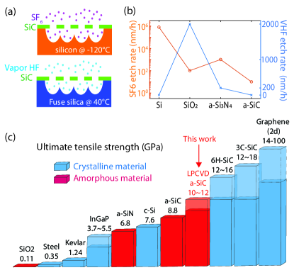
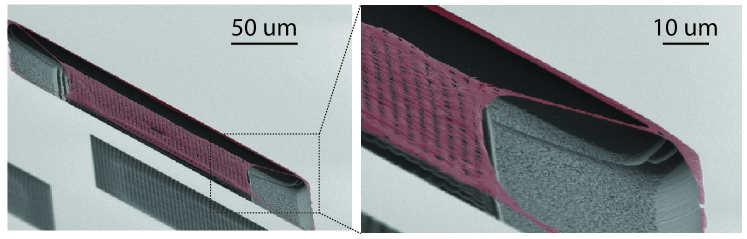
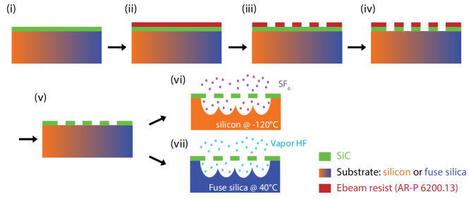
Better chemical stability and inertness of the sensing components can significantly improve the sensors’ reliability, particularly for their operation under chemically harsh environments. Meanwhile, thin film materials’ chemical inertness allows them to be deposited on various substrates, patterned, and then suspended as nanomechanical resonators by removing the substrate underneath (i.e. undercutting). A high selectivity between the thin film and the substrate allows for higher yield and accuracy in fabricating suspended nanostructures . Similar to their crystalline counterpart, LPCVD a-SiC thin films have been reported to have very high chemical inertness to various wet etchants [43]. Likewise, we found that a-SiC also has high chemical inertness to the widely used dry etchants, such as SF6 isotropic plasma etching for silicon substrate, and vapor hydrofluoric acid etching for silicon oxide substrate, as illustrated in Figure 1(a). The excellent chemical stability implies high selectivity between a-SiC and various commonly used substrates during undercutting, as shown in Figure 1(b). Dry etchants are preferred for suspending high-aspect-ratio nanomechanical structures, since they help to avoid stiction during liquid etchant evaporation and thus improve the yield rate of working devices. To take advantage of the superior chemical inertness, we fabricated nanomechanical resonators with continuous films down to 5nm, as shown in SEM pictures in Supporting Information (F).
Moreover, the undercut method based on dry etchants introduces little perturbation to the suspended nano-structure, making it possible to perform tensile testing on chips. In Section IV, we fabricate suspended nano-structures with different maximum tensile stresses to accurately determine the ultimate tensile strength (UTS) of a-SiC films. As a result, we demonstrate that a-SiC films have UTS up to 10-12 GPa, which are the highest among amorphous materials after patterning and are approaching the UTS of strong materials like c-SiC [24] and graphene nano-ribbons [19], both of which are known for their high UTS. The comparison of UTS between LPCVD a-SiC and other materials commonly used for nanomechanics is shown in Figure 1(c).
III Mechanical property characterization with resonance method
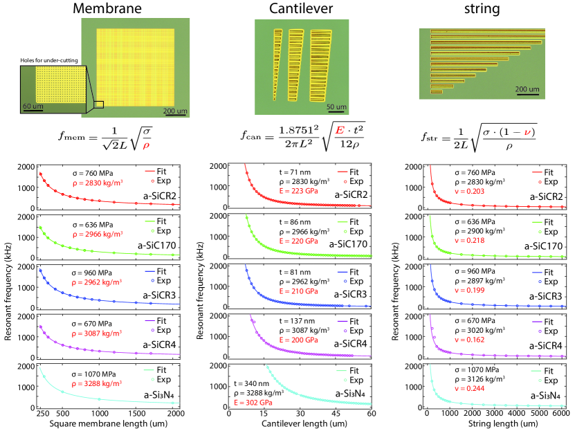
In order to design desired nanomechanical resonators with a specific thin film material, it is necessary to accurately characterize the material’s mechanical parameters, such as film stress, Young’s modulus, Poisson ratio and density. Various methods are developed to measure these parameters, including static methods, like nano-indentation [78, 79] and dynamic methods like resonance response [80, 81, 82, 83]. Many studies aiming to design high-performance nanomechanical resonators have relied on mechanical parameter values obtained from literature without considering potential variations of thin film properties due to different deposition environments, such as commonly used materials like a-Si3N4 [10, 12], c-Si [14], and c-SiC [15, 16]. While these adaptations are usually reasonable and align well with experimental results, characterizing the exact parameters of the materials used would be beneficial when exploring the optimal performance of nanomechanical resonators [84, 80]. In this section, we present a simple and universal method to systematically characterize the important mechanical parameters of LPCVD a-SiC thin films.
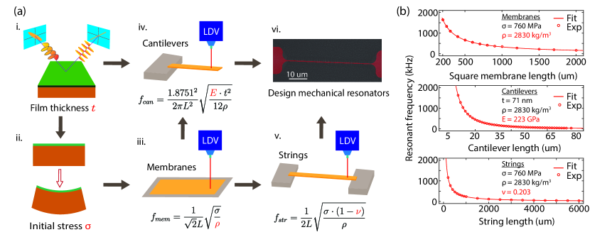
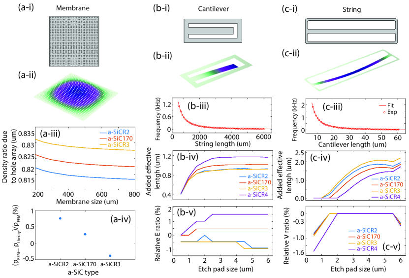
The characterization flow of the method begins with measuring the thickness of the a-SiC thin film () after LPCVD deposition using a spectroscopic ellipsometer, which is an optical technique to confirm the thin film thickness and investigate its dielectric properties simultaneously. We then identify the film stress () using the wafer bending method. After dicing the wafer into small chips, we pattern the a-SiC thin film and suspend it in the form of membranes, cantilevers, and strings with different lengths (). The suspended nanomechanical resonators are measured with a laser Doppler vibrometer (LDV) in the vacuum environment down to mbar. The measured resonant frequencies of the fundamental modes of the membranes (), cantilevers (), and strings () can be fitted with their corresponding analytical expressions, which reveal the Young’s modulus (), Poisson ratio (), and density () of the a-SiC thin film, respectively. During the fitting process, finite element method (FEM) simulation is used to describe the patterned resonators more precisely by taking into account the holes on the membranes and the overhangs from under-cutting adjacent to the cantilevers and strings. More detailed information about the measurements, analytical fitting, and simulations are shown in Supporting Information (A) and (B).
Using the above measurements, we can characterize the important mechanical parameters of LPCVD a-SiC thin films, then design and fabricate nanomechanical resonators with desired performance. Note that this straightforward and non-contact method can be universally applied to characterize the mechanical properties of other tensile thin film materials that can be fabricated into resonators with various geometries, i.e. cantilevers, strings, and membranes. This allows for quality control of thin films deposited in different batches or under varied deposition environments. As a result, nanomechanical resonators manufactured for various applications can be characterized in an efficient and economical manner, resulting in higher reliability for both industrial and academic applications. With all the relevant mechanical parameters accurately measured, we can fabricate a series of suspended devices specifically designed for characterizing the ultimate tensile strengths of a-SiC thin films in the following section.
| Recipe | GFR | P (mTorr) | Substrate | (nm) | (MPa) | (kg/m3) | (GPa) | UTS (GPa) | ||
|---|---|---|---|---|---|---|---|---|---|---|
| a-SiCR2 | 2 | 600 | Silicon | 71 | 760 | 2830 | 223 | 0.203 | 5175 | 12.04 |
| a-SiCR2FS | 2 | 600 | Fuse Silica | 71∗ | 1596 | 2830∗ | 223∗ | 0.203∗ | 4554 | 12.04∗ |
| a-SiC170 | 2 | 170 | Silicon | 86 | 636 | 2966 | 220 | 0.218 | 4485 | 10.27 |
| a-SiCR3 | 3 | 600 | Silicon | 81 | 960 | 2962 | 210 | 0.199 | 4692 | 11.12 |
| a-SiCR4 | 4 | 600 | Silicon | 137 | 670 | 3087 | 200 | 0.162 | 1035 | 3.5 |
∗ Parameters of a-SiCR2FS are adapted from a-SiCR2 due to its transparent substrate
IV Ultimate Tensile Strength of amorphous SiC
Ultimate tensile strength (UTS), or sometimes coinciding with yield strength for brittle materials such as a-SiC [35], describes the maximum tensile stress a material can endure before breaking while being stretched. Materials with higher UTS not only allows them to operate more reliably as mechanical sensors or coating in harsh environments, but also enlarges the design space for nanomechanical resonators. High UTS has been shown for nanowires fabricated with various materials, whose small cross-section areas minimize the appearance of defects [85, 86], and for nanomechanical membranes without nano-patterning to avoid the presence of rough sidewalls [87]. However, both scenarios above do not allow for further shape modification, reducing interest in their potential for various applications. While the crystalline form of materials usually tend to be mechanically stronger than their amorphous forms due to long-range order, examples such as glassy metal [88] and synthesized AM-III carbon [89] demonstrate extraordinary mechanical properties comparable to their celebrated crystalline counterparts in terms of fracture toughness and yield strength, or hardness and compressive strength, respectively. This correspondence remains between c-SiC and a-SiC. While c-SiC has shown a UTS as high as 12-18 GPa via micro-pillars so far [24], a-SiC nanowires have been measured to have a UTS up to 8.8 GPa via a tensile test with its two ends fixed by silver epoxy [35], which is higher than the ones shown for LPCVD a-Si3N4 (6.8 GPa [23]) and Si (7.6 GPa [70]).
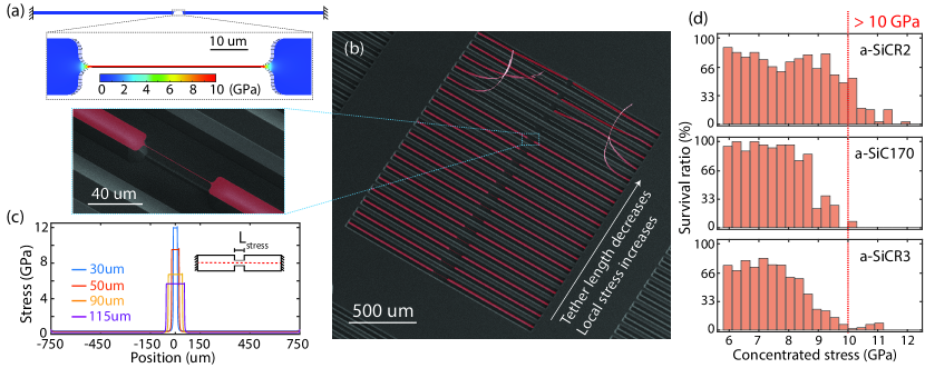
With the aim of characterizing the design space of nanomechanical resonators using LPCVD a-SiC thin film, we characterized its UTS by geometrically tapering the suspended a-SiC thin film in order to concentrate the tensile stress up to the fracture point. Unlike other tensile test methods [90], the presented method allows to determine the UTS of the tensile nanostructured film accurately, while avoiding the ambiguity caused by external loads, glues, and limitations of nano-fabrication, e.g. limited accuracy of nano-patterning and stiction during wet undercut. With the mechanical parameters characterized in Section III, a-SiC hourglass-shaped devices consisting of a short and narrow tether surrounded by long and wide pads on both sides which are designed and suspended to measure the UTS of LPCVD a-SiC thin films. The devices have a total length of 1500um, with pads on both sides that have a width of 15 um, and the middle tethers that have varying lengths and a width of 500 nm, as shown in Figure 3(a). After being suspended with dry etchants, the tensile stress on the hourglass-shaped device will redistribute and result in an increase of stress on the middle tether due to the pulling of the pads caused by residual stresses arising from the fabrication. The re-distributed stress profile in Figure 3(a) is obtained via finite element method (FEM). The devices are designed to have varying tether lengths from short to long, which are then arranged adjacently as shown in Figure 3(b).
To establish a force equilibrium between the tether and the pads on each device, the ratio between the tensile stresses on the tether and the pads is inversely proportional to the ratio between their widths, combined with a small proportion of the lengths between the two, which enhances the strain (percentage of elongation) on the tether, the tensile stress on the tether in our hourglass-shaped devices can be significantly amplified during stress relaxation after suspending. As shown with FEM simulation in Figure 3(c), devices with shorter tether lengths contain higher maximum concentrated tensile stresses on the tethers. This method allows the determination of the UTS of the nanostructured a-SiC thin films by counting the number of surviving devices after suspension. As shown in Figure 3(b), a series of hourglass-shaped devices are fabricated with a-SiCR2. The 18 devices have tether lengths ranging from 30 to 115 um, corresponding to stresses from 12.53 to 5.97 GPa, respectively. The adjacent devices have tether lengths that differ for 5 um, the shorter the tethers are, the larger difference in concentrated stress the devices contain, e.g. the concentrated stress difference between devices with 115 um and 110 um tether lengths is 0.18 GPa, while one between devices with 35 um and 30 um is 0.72 GPa. In the case of each a-SiC thin film, the survival rate of each tensile interval shown in Figure 3(d) is determined, by employing 36 to 72 devices for testing.
The survival of the suspending hour-glass-shaped device with the tether length below 50 um, corresponds to a UTS above 10 GPa for a-SiCR2. Similarly, we can identify the UTS for all a-SiC thin films used in this study to be higher than 10 GPa, as shown in the histograms of ratios of survival devices in Figure 3(d). The histograms also show that, with relatively higher deposition pressure and lower gas flow ratios, a maximum UTS up to 12 GPa can be achieved with a-SiCR2, which is almost twice that of the UTS shown for nanostructured LPCVD a-Si3N4 films. The measured UTS of a-SiCR4 is below 3.5 GPa, which is not attractive for further characterization. In the future, with a larger number of fabricated devices and a denser range of tether lengths, one can determine the UTS of the LPCVD a-SiC thin films more precisely. In practice, the nanopatterning with electron beam lithography can readily achieve an accuracy of 10 nm, which allows for the method’s accuracy to be as low as 1.2 MPa on a-SiCR2, i.e. an error of less than 0.2% when measuring the UTS. Higher UTS is found for recipes deposited with lower gas flow ratios (a-SiCR2/3/4), which might due to a higher carbon composition in the thin film [73], and C-C chemical bonds are stronger than Si-C and Si-Si bonds [91]. For a-SiC films deposited with different pressure, a-SiCR2 (600 mTorr) is found to have a higher UTS, while a-SiC170 (170 mTorr) exhibits better yield under lower concentrated stresses as shown by the survival rates. According to the relationship between strength and Young’s modulus of SiC shown in [35], UTS (or fracture strength) is 5.3% of , therefore the theoretically predicted UTS for a-SiCR2/a-SiC170/a-SiCR3, are 11.82/11.66/11.13 GPa, respectively, matching well with the experimentally extracted data from the survived devices 12.04/10.27/11.12 GPa shown in Table 1. The small offset for the values of a-SiC170 may be due to its rougher surface as shown in Supporting Information (G).
With strain engineering techniques, one can amplify the mechanical quality factor of a nanomechanical resonator by boosting their dissipation dilution factor , where is the intrinsic quality factor of the thin film material [92, 10]. Since the upper bound for of a nanomechanical string vibrating at a certain frequency is given by , where denotes the UTS of the thin film material [93], thin film materials with higher UTS and lower thickness are advantageous to obtain a higher . Among all a-SiC thin films shown in this work, a-SiCR2 is the most promising one to maximize the factor, thanks to its high and UTS. The superior chemical resistivity of a-SiC enables the fabrication of thin films into suspending resonators with a thickness as low as 5 nm (shown in Supporting Information (F)). This combined with its elevated ultimate tensile strength , which measures above 10 GPa in thicker films, makes a-SiC string resonators highly promising in achieving a supreme upper bound for at a certain frequency .
V Intrinsic Quality Factor and High Q Mechanical Resonators
In this section we characterize the intrinsic quality factor of LPCVD a-SiC, then design and fabricate high-Q nanomechanical resonators with it. High mechanical quality (Q) factor nanomechanical resonators are desirable for various applications, ranging from precise force/acceleration sensing [6, 1], microwave-to-optical conversion [67], to quantum optomechanics [66, 94]. Following the method introduced by LIGO [95], the field of strain engineering is advancing rapidly, boosting the Q factor of nanomechanical resonators by several orders of magnitude. A variety of strategies have been proposed aiming to improve the Q factors of tensile-loaded nanomechanical resonators. These include patterning 2D geometries appropriately [9, 11, 13, 12, 96, 97, 98], modifying mass distribution [99, 2] and mode of interest (e.g., from fundamental to higher order or from flexural to torsional modes [2]), in-situ annealing for surface cleaning [100], as well as cooling down to cryogenic temperatures [101, 14]. The methods mentioned above can benefit from utilizing the LPCVD a-SiC thin film we characterized in this work, due to its high deposition film tensile stress, superior chemical resistivity, and impressive ultimate tensile strength.
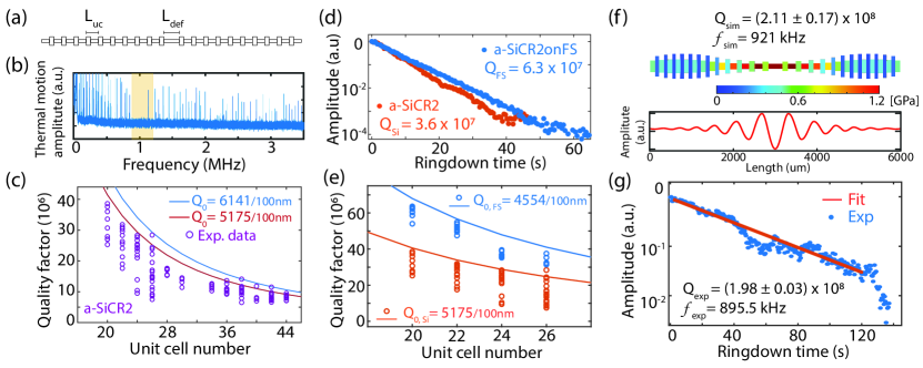
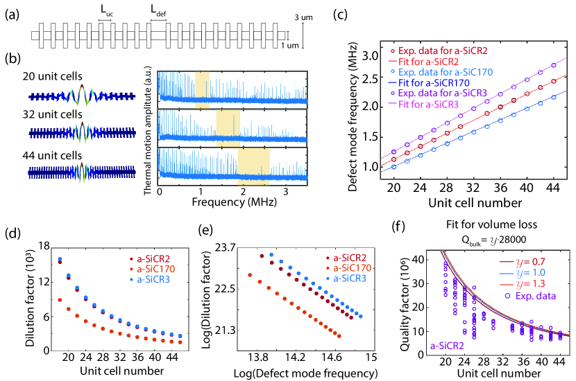
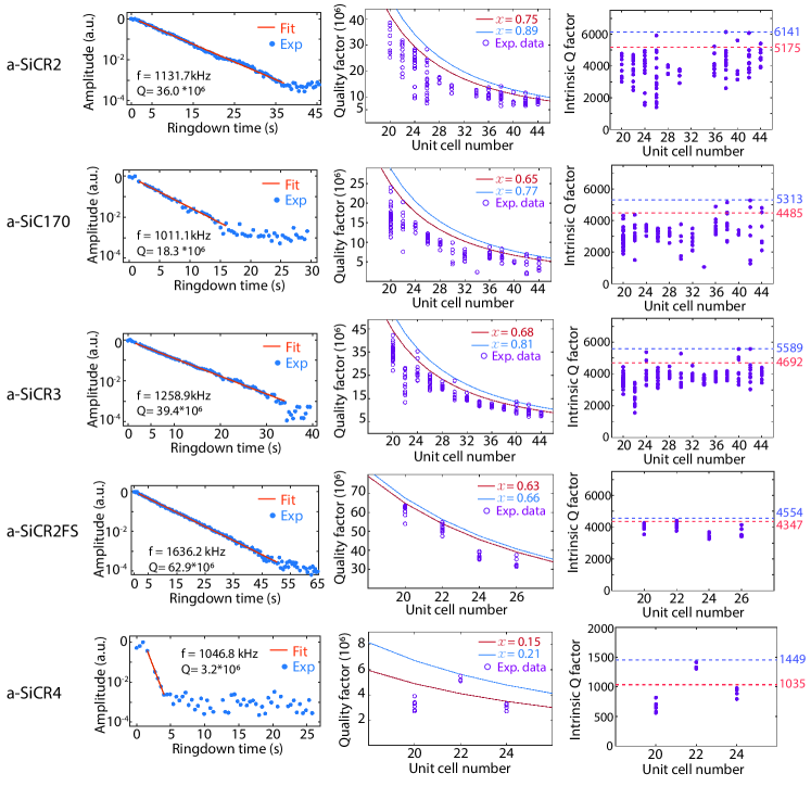
The intrinsic quality factors of a-SiC thin films are identified by experimentally measuring the Q factors of phononic crystal (PnC) nanostrings [10], whose many spurious loss mechanisms are eliminated, and dissipation dilution factor is well defined, leading to an expected intrinsic Q factor . For thin nanomechanical resonators, can be assumed to depend linearly on the film thickness, since it is predominantly determined by surface loss rather than bulk loss [92]. We fabricate a series of uniformly corrugated high-aspect-ratio (PnC) nanostrings with a length of 4 mm, varying unit-cell lengths and defect lengths in the middle (Figure 4(a)), leading to PnC nanostrings with unit-cell numbers from 20 to 44. The widths of the wide and narrow parts of the nanostrings are 3 um and 1 um respectively. The vibration amplitude of the nanostrings as a function of frequency is acquired (Figure 4(b)) with a custom balanced homodyne detection interferometer at the vacuum environment of mbar (see Supporting Information (I)). Using the ringdown method, the Q factors of defect modes for each PnC nanostring are measured. For example, the ones of 10 unit-cells PnC nanostrings fabricated wtih a-SiCR2 and a-SiCR2FS are plotted in Figure 4(d). Using FEM simulation, the dilution factor of each PnC nanostring geometry can be numerically calculated. Together with the Q factors of the corresponding nanostring measured experimentally, the intrinsic Q factor of the different a-SiC thin films are determined. For example, the of a-SiCR2 and a-SiCR2FS are shown in Figure 4(c) and (e) respectively. The of the other a-SiC films are shown in Table 1, and the corresponding measurement data can be found in Supporting Information (D). In order to compare the of a-SiC thin films with different thicknesses, we present them with the unit per 100 nm, as of a thin film is shown to be a function of thickness [84]. Deposited with the same recipe, a-SiCR2 (5175/100 nm) and a-SiCR2FS (4554/100 nm) have similar . The similar performance on the transparent substrate allows for integrating high-Q nanomechanical sensors into free-space optical systems in a practical manner. By reasonably assuming the films have similar mechanical properties on different substrates, a-SiCR2FS is measured to have a deposition stress of 1596 MPa, a factor of two higher than a-SiCR2 due to a larger thermal expansion coefficients difference between the a-SiC thin film and fused silica substrate. Worth noting is that the of a-SiCR2 is the highest among all LPCVD a-SiC investigated, indicating that a lower gas flow ratio (GFR=2), i.e., more carbon content [73], and a moderate deposition pressure (600 mTorr) is beneficial to have better film quality.
To exploit the sensing potential of LPCVD a-SiC, we designed and optimized a tapered PnC nanostring with a length of 6mm and a thickness of 71 nm using a a-SiCR2 thin film. Bayesian optimization [12] was used to find designs with high Q-factor – more details can be found in Supporting Information (E). This simulation-based optimization is largely possible due to the accurate characterization of the material properties of the a-SiC thin films in previous sections. As shown in Figure 4(f), the optimized PnC nanostring consists of fixed 24 unit cells with different widths and lengths, leading to a stress concentration of up to 1.2 GPa towards its center part. Within the phononic bandgap generated by the optimized tapered PnC nanostring, a soft clamped defect mode with a simulated Q factor appears at the frequency of kHz, as shown at the bottom of Figure 4(f). The optimized tapered PnC nanostring was fabricated based on the design at the top of Figure 4(f), and it was measured at an interferometer under ultra-high vacuum of mbar. As a result, an high Q factor mechanical mode with was measured experimentally at a frequency of kHz at room temperature, shown by its ringdown curve plotted in Figure 4(g). This result demonstrates, for the first time, a mechanical quality factor exceeding for silicon carbide nanomechanical resonators, as predicted by simulation. This also suggests that future design strategies to enhance resonator performance can be carried out using the LPCVD a-SiC thin films.
In addition, the quality factor-frequency product of the optimized LPCVD a-SiC tapered PnC nanostring is , which is significantly higher than the quantum limit . This paves the way towards engineering quantum states in room temperature environments [94, 9]. This high quality factor of the nanomechanical resonator with an effective mass kg corresponds to a force sensitivity of 7.7 aN/Hz1/2 at room temperature, which is comparable to a typical atomic force microscope cantilever operating at liquid helium temperature. With the high quality factor shown above, LPCVD a-SiC is shown to be the third material that can reach at room temperature using strain engineering, after conventional a-Si3N4 [10] and strained silicon [14]. Moreover, the superior chemical and mechanical properties of LPCVD a-SiC allow for the fabrication of thinner and stronger resonators, enabling it to be more compatible with the dissipation dilution method. With advantages such as a relatively simple and low-cost fabrication process, compatibility with various substrates, including transparent ones, and its potential to perform better and more stably in harsh environments as high-Q nanomechanical resonators, LPCVD a-SiC is a promising material for fabricating commercial mechanical sensors.
VI Conclusion and outlook
In summary, our study has uncovered an amorphous silicon carbide thin film with a ultimate tensile strength above 10 GPa, the highest value ever measured for a nanostructured amorphous material and approaching the experimental values shown by graphene nano-ribbons [19]. Their robustness to chemicals allow us to fabricate nanostructures with very high fidelity even when their geometries make them delicate high-aspect-ratio structures. This ability to produce structures with high fidelity also allow us to measure the film’s mechanical properties with high precision. We deposit amorphous silicon carbide in varying deposition conditions and substrates to understand new approaches towards increasing ultimate yield strength. Then using the a-SiC with the highest UTS, we designed and fabricated a variety of well-understood nanostructures such as cantilever, membranes and doubly-clamped strings to measure the thin films mechanical properties such as density, Young’s modulus, Poisson ratio, and mechanical loss tangents. For the latter we employ nanostrings patterned with phononic bandstructures which conventionally have some of the lowest mechanical dissipations in literature, and this allows us to measure very low mechanical dissipation. The a-SiC nanostrings support soft-clamped mechanical modes with quality factors exceeding at room temperature; a new regime for SiC devices and on par with the state-of-the-art SiN resonators. This corresponds to a high force sensitivity of 7.7 aN/Hz1/2. We demonstrate a robust characterization process based on the simple fabrication and optical techniques which does not rely on complex tension loading setups.
The discovery of this amorphous SiC material represents an advancement in the field of high-strength material science which is conventionally dominated by crystalline and 2D materials. However, our findings demonstrate that amorphous materials have the potential to surpass crystalline materials in certain applications due to their inherently isotropic mechanical properties, which allow for more design freedom and ease of fabrication. The high ultimate tensile strength of this amorphous material is particularly attractive for mechanical sensors, as it enables greater flexibility in strain engineering. This discovery opens up new possibilities for the use of amorphous materials in a variety of high-performance applications.
Acknowledgements.
We wish to acknowledge Peter G. Steeneken, Gerard Verbiest, and Martin Lee for their helpful suggestions on the manuscript and their support of our project. We want to thank Satadal Dutta, Ali Sarafraz, Matthijs de Jong for the helpful discussions. M.X. and R.N. also thank the staffs of both the Kavli Nanolab Delft and the Else Kooi Lab, in particular from C. de Boer, for supporting our fabrication efforts. This publication is part of the project, Probing the physics of exotic superconductors with microchip Casimir experiments (740.018.020) of the research programme NWO Start-up which is partly financed by the Dutch Research Council (NWO).This work has received funding from the EMPIR programme co-financed by the Participating States and from the European Union’s Horizon 2020 research and innovation programme (No. 17FUN05 PhotoQuant). R.N. would like to acknowledge support from the Limitless Space Institute’s I2 Grant.References
- Krause et al. [2012] A. G. Krause, M. Winger, T. D. Blasius, Q. Lin, and O. Painter, A high-resolution microchip optomechanical accelerometer, Nature Photonics 6, 768 (2012).
- Pratt et al. [2023] J. R. Pratt, A. R. Agrawal, C. A. Condos, C. M. Pluchar, S. Schlamminger, and D. J. Wilson, Nanoscale torsional dissipation dilution for quantum experiments and precision measurement, Physical Review X 13, 011018 (2023).
- Manzaneque et al. [2022] T. Manzaneque, M. K. Ghatkesar, F. Alijani, M. Xu, R. A. Norte, and P. G. Steeneken, Resolution limits of resonant sensors with duffing non-linearity, arXiv preprint arXiv:2205.11903 (2022).
- Garcia-Sanchez et al. [2012] D. Garcia-Sanchez, K. Y. Fong, H. Bhaskaran, S. Lamoreaux, and H. X. Tang, Casimir force and in situ surface potential measurements on nanomembranes, Physical review letters 109, 027202 (2012).
- Pate et al. [2020] J. M. Pate, M. Goryachev, R. Y. Chiao, J. E. Sharping, and M. E. Tobar, Casimir spring and dilution in macroscopic cavity optomechanics, Nature Physics 16, 1117 (2020).
- Hälg et al. [2021] D. Hälg, T. Gisler, Y. Tsaturyan, L. Catalini, U. Grob, M.-D. Krass, M. Héritier, H. Mattiat, A.-K. Thamm, R. Schirhagl, et al., Membrane-based scanning force microscopy, Physical Review Applied 15, L021001 (2021).
- Reinhardt et al. [2016] C. Reinhardt, T. Müller, A. Bourassa, and J. C. Sankey, Ultralow-noise sin trampoline resonators for sensing and optomechanics, Physical Review X 6, 021001 (2016).
- Verbridge et al. [2006] S. S. Verbridge, J. M. Parpia, R. B. Reichenbach, L. M. Bellan, and H. G. Craighead, High quality factor resonance at room temperature with nanostrings under high tensile stress, Journal of Applied Physics 99, 124304 (2006).
- Norte et al. [2016] R. A. Norte, J. P. Moura, and S. Gröblacher, Mechanical resonators for quantum optomechanics experiments at room temperature, Physical review letters 116, 147202 (2016).
- Ghadimi et al. [2018] A. H. Ghadimi, S. A. Fedorov, N. J. Engelsen, M. J. Bereyhi, R. Schilling, D. J. Wilson, and T. J. Kippenberg, Elastic strain engineering for ultralow mechanical dissipation, Science 360, 764 (2018).
- Fedorov et al. [2020] S. A. Fedorov, A. Beccari, N. J. Engelsen, and T. J. Kippenberg, Fractal-like mechanical resonators with a soft-clamped fundamental mode, Physical Review Letters 124, 025502 (2020).
- Shin et al. [2022] D. Shin, A. Cupertino, M. H. de Jong, P. G. Steeneken, M. A. Bessa, and R. A. Norte, Spiderweb nanomechanical resonators via bayesian optimization: inspired by nature and guided by machine learning, Advanced Materials 34, 2106248 (2022).
- Bereyhi et al. [2022] M. J. Bereyhi, A. Arabmoheghi, A. Beccari, S. A. Fedorov, G. Huang, T. J. Kippenberg, and N. J. Engelsen, Perimeter modes of nanomechanical resonators exhibit quality factors exceeding at room temperature, Physical Review X 12, 021036 (2022).
- Beccari et al. [2022] A. Beccari, D. A. Visani, S. A. Fedorov, M. J. Bereyhi, V. Boureau, N. J. Engelsen, and T. J. Kippenberg, Strained crystalline nanomechanical resonators with quality factors above 10 billion, Nature Physics 18, 436 (2022).
- Romero et al. [2020] E. Romero, V. M. Valenzuela, A. R. Kermany, L. Sementilli, F. Iacopi, and W. P. Bowen, Engineering the dissipation of crystalline micromechanical resonators, Physical Review Applied 13, 044007 (2020).
- Klaß [2022] Y. S. Klaß, High Q nanomechanical resonators fabricated from crystalline silicon carbide, Ph.D. thesis, Technische Universität München (2022).
- Manjeshwar et al. [2022] S. K. Manjeshwar, A. Ciers, F. Hellman, J. Bläsing, A. Strittmater, and W. Wieczorek, Micromechanical high-q trampoline resonators from strained crystalline ingap for integrated free-space optomechanics, arXiv preprint arXiv:2211.12469 (2022).
- Wu et al. [2021] Q. Wu, X. Yan, Y. Jia, and X. Yao, Defective carbon-based materials: controllable synthesis and electrochemical applications, EnergyChem 3, 100059 (2021).
- Goldsche et al. [2018] M. Goldsche, J. Sonntag, T. Khodkov, G. J. Verbiest, S. Reichardt, C. Neumann, T. Ouaj, N. von den Driesch, D. Buca, and C. Stampfer, Tailoring mechanically tunable strain fields in graphene, Nano letters 18, 1707 (2018).
- Cao et al. [2020] K. Cao, S. Feng, Y. Han, L. Gao, T. Hue Ly, Z. Xu, and Y. Lu, Elastic straining of free-standing monolayer graphene, Nature communications 11, 284 (2020).
- Gu et al. [2013] X. W. Gu, Z. Wu, Y.-W. Zhang, D. J. Srolovitz, and J. R. Greer, Microstructure versus flaw: mechanisms of failure and strength in nanostructures, Nano letters 13, 5703 (2013).
- Zhao et al. [2022] X. Zhao, B. Mao, M. Liu, J. Cao, S. J. Haigh, D. G. Papageorgiou, Z. Li, and R. J. Young, Controlling and monitoring crack propagation in monolayer graphene single crystals, Advanced Functional Materials 32, 2202373 (2022).
- Bereyhi et al. [2019] M. J. Bereyhi, A. Beccari, S. A. Fedorov, A. H. Ghadimi, R. Schilling, D. J. Wilson, N. J. Engelsen, and T. J. Kippenberg, Clamp-tapering increases the quality factor of stressed nanobeams, Nano letters 19, 2329 (2019).
- Kwon et al. [2015] G. Kwon, H.-H. Jo, S. Lim, C. Shin, H.-H. Jin, J. Kwon, and G.-M. Sun, Room-temperature yield and fracture strength of single-crystalline 6h silicon carbide, Journal of materials science 50, 8104 (2015).
- Rasool et al. [2013] H. I. Rasool, C. Ophus, W. S. Klug, A. Zettl, and J. K. Gimzewski, Measurement of the intrinsic strength of crystalline and polycrystalline graphene, Nature communications 4, 2811 (2013).
- Zhang et al. [2015] T. Zhang, X. Li, and H. Gao, Fracture of graphene: a review, International Journal of Fracture 196, 1 (2015).
- Lee et al. [2008] C. Lee, X. Wei, J. W. Kysar, and J. Hone, Measurement of the elastic properties and intrinsic strength of monolayer graphene, science 321, 385 (2008).
- Wang et al. [2012] M. Wang, C. Yan, L. Ma, N. Hu, and M. Chen, Effect of defects on fracture strength of graphene sheets, Computational Materials Science 54, 236 (2012).
- Xu et al. [2018] J. Xu, G. Yuan, Q. Zhu, J. Wang, S. Tang, and L. Gao, Enhancing the strength of graphene by a denser grain boundary, ACS nano 12, 4529 (2018).
- Qu et al. [2012] R. Qu, M. Calin, J. Eckert, and Z. Zhang, Metallic glasses: Notch-insensitive materials, Scripta Materialia 66, 733 (2012).
- Jiang et al. [2021] H. Jiang, T. Shang, H. Xian, B. Sun, Q. Zhang, Q. Yu, H. Bai, L. Gu, and W. Wang, Structures and functional properties of amorphous alloys, Small Structures 2, 2000057 (2021).
- Greer [1995] A. L. Greer, Metallic glasses, Science 267, 1947 (1995).
- Telford [2004] M. Telford, The case for bulk metallic glass, Materials today 7, 36 (2004).
- Wong et al. [1997] E. W. Wong, P. E. Sheehan, and C. M. Lieber, Nanobeam mechanics: elasticity, strength, and toughness of nanorods and nanotubes, science 277, 1971 (1997).
- Cui et al. [2019] J. Cui, Z. Zhang, H. Jiang, D. Liu, L. Zou, X. Guo, Y. Lu, I. P. Parkin, and D. Guo, Ultrahigh recovery of fracture strength on mismatched fractured amorphous surfaces of silicon carbide, ACS nano 13, 7483 (2019).
- Wijesundara and Azevedo [2011] M. Wijesundara and R. Azevedo, Silicon carbide microsystems for harsh environments, Vol. 22 (Springer Science & Business Media, 2011).
- Gerhardt [2011] R. Gerhardt, Properties and applications of silicon carbide (BoD–Books on Demand, 2011).
- Kimoto and Cooper [2014] T. Kimoto and J. A. Cooper, Fundamentals of Silicon Carbide Technology: Growth, Characterization, Devices and Applications (Wiley-IEEE Press, 2014).
- Yi et al. [2020] A. Yi, Y. Zheng, H. Huang, J. Lin, Y. Yan, T. You, K. Huang, S. Zhang, C. Shen, M. Zhou, et al., Wafer-scale 4h-silicon carbide-on-insulator (4h–sicoi) platform for nonlinear integrated optical devices, Optical Materials 107, 109990 (2020).
- Martini and Politi [2017] F. Martini and A. Politi, Linear integrated optics in 3c silicon carbide, Optics Express 25, 10735 (2017).
- Powell et al. [2022] K. Powell, L. Li, A. Shams-Ansari, J. Wang, D. Meng, N. Sinclair, J. Deng, M. Lončar, and X. Yi, Integrated silicon carbide electro-optic modulator, Nature Communications 13, 1851 (2022).
- Saddow and Agarwal [2004] S. E. Saddow and A. K. Agarwal, Advances in silicon carbide processing and applications (Artech House, 2004).
- Morana et al. [2013] B. Morana, G. Pandraud, J. Creemer, and P. Sarro, Characterization of lpcvd amorphous silicon carbide (a-sic) as material for electron transparent windows, Materials Chemistry and Physics 139, 654 (2013).
- Iliescu and Poenar [2012] C. Iliescu and D. P. Poenar, Pecvd amorphous silicon carbide (-sic) layers for mems applications, in Physics and Technology of Silicon Carbide Devices (IntechOpen, 2012).
- Fraga et al. [2012] M. A. Fraga, R. S. Pessoa, M. Massi, and H. S. Maciel, Applications of sic-based thin films in electronic and mems devices, Physics and technology of silicon carbide devices 1, 313 (2012).
- Blank et al. [1999] V. Blank, M. Popov, G. Pivovarov, N. Lvova, and S. Terentev, Mechanical properties of different types of diamond, Diamond and related materials 8, 1531 (1999).
- Dang et al. [2021] C. Dang, J.-P. Chou, B. Dai, C.-T. Chou, Y. Yang, R. Fan, W. Lin, F. Meng, A. Hu, J. Zhu, et al., Achieving large uniform tensile elasticity in microfabricated diamond, Science 371, 76 (2021).
- Papageorgiou et al. [2017] D. G. Papageorgiou, I. A. Kinloch, and R. J. Young, Mechanical properties of graphene and graphene-based nanocomposites, Progress in materials science 90, 75 (2017).
- Blum et al. [1999] T. Blum, B. Dresler, M. Hoffmann, et al., Wear-resistant amorphous sic coatings produced by plasma-enhanced cvd, Surface and Coatings Technology 116, 1024 (1999).
- Jiang et al. [1999] L. Jiang, X. Chen, X. Wang, L. Xu, F. Stubhan, and K.-H. Merkel, a-sicx: H films deposited by plasma-enhanced chemical vapor deposition at low temperature used for moisture and corrosion resistant applications, Thin Solid Films 352, 97 (1999).
- Flannery et al. [1998] A. F. Flannery, N. J. Mourlas, C. W. Storment, S. Tsai, S. H. Tan, J. Heck, D. Monk, T. Kim, B. Gogoi, and G. T. Kovacs, Pecvd silicon carbide as a chemically resistant material for micromachined transducers, Sensors and Actuators A: Physical 70, 48 (1998).
- Buijtendorp et al. [2022] B. Buijtendorp, S. Vollebregt, K. Karatsu, D. Thoen, V. Murugesan, K. Kouwenhoven, S. Hähnle, J. Baselmans, and A. Endo, Hydrogenated amorphous silicon carbide: A low-loss deposited dielectric for microwave to submillimeter-wave superconducting circuits, Physical Review Applied 18, 064003 (2022).
- Köhler et al. [2021] M. Köhler, M. Pomaska, P. Procel, R. Santbergen, A. Zamchiy, B. Macco, A. Lambertz, W. Duan, P. Cao, B. Klingebiel, et al., A silicon carbide-based highly transparent passivating contact for crystalline silicon solar cells approaching efficiencies of 24%, Nature Energy 6, 529 (2021).
- Tawada et al. [1982] Y. Tawada, M. Kondo, H. Okamoto, and Y. Hamakawa, Hydrogenated amorphous silicon carbide as a window material for high efficiency a-si solar cells, Solar Energy Materials 6, 299 (1982).
- van Cleef et al. [1998] M. W. van Cleef, F. A. Rubinelli, R. Rizzoli, R. Pinghini, R. E. Schropp, and W. F. van der Weg, Amorphous silicon carbide/crystalline silicon heterojunction solar cells: a comprehensive study of the photocarrier collection, Japanese journal of applied physics 37, 3926 (1998).
- Sarro [2000] P. M. Sarro, Silicon carbide as a new mems technology, Sensors and Actuators A: Physical 82, 210 (2000).
- Fraga and Pessoa [2020] M. Fraga and R. Pessoa, Progresses in synthesis and application of sic films: From cvd to ald and from mems to nems, Micromachines 11, 799 (2020).
- Barnes et al. [2012] A. C. Barnes, C. A. Zorman, and P. X. Feng, Amorphous silicon carbide (-sic) thin square membranes for resonant micromechanical devices, in Materials Science Forum, Vol. 717 (Trans Tech Publ, 2012) pp. 533–536.
- Xing et al. [2019] P. Xing, D. Ma, K. J. Ooi, J. W. Choi, A. M. Agarwal, and D. Tan, Cmos-compatible pecvd silicon carbide platform for linear and nonlinear optics, ACS Photonics 6, 1162 (2019).
- Lee et al. [2015] J. Y. Lee, X. Lu, and Q. Lin, High-q silicon carbide photonic-crystal cavities, Applied Physics Letters 106, 041106 (2015).
- Xing et al. [2020] P. Xing, D. Ma, L. C. Kimerling, A. M. Agarwal, and D. T. Tan, High efficiency four wave mixing and optical bistability in amorphous silicon carbide ring resonators, APL Photonics 5, 076110 (2020).
- Auditore et al. [2002] A. Auditore, C. Satriano, U. Coscia, G. Ambrosone, V. Parisi, and G. Marletta, Human serum albumin adsorption onto a-sic: H and ac: H thin films deposited by plasma enhanced chemical vapor deposition, Biomolecular Engineering 19, 85 (2002).
- Saddow [2016] S. Saddow, Silicon Carbide Biotechnology, Second Edition: A Biocompatible Semiconductor for Advanced Biomedical Devices and Applications (Elsevier, 2016).
- Bauser et al. [2022] H. C. Bauser, M. D. Foley, M. E. Phelan, W. Weigand, D. R. Needell, Z. C. Holman, and H. A. Atwater, Amorphous silicon carbide high contrast gratings as highly efficient spectrally selective visible reflectors, Optics Express 30, 26787 (2022).
- Deku et al. [2018] F. Deku, C. L. Frewin, A. Stiller, Y. Cohen, S. Aqeel, A. Joshi-Imre, B. Black, T. J. Gardner, J. J. Pancrazio, and S. F. Cogan, Amorphous silicon carbide platform for next generation penetrating neural interface designs, Micromachines 9, 480 (2018).
- Teufel et al. [2009] J. D. Teufel, T. Donner, M. Castellanos-Beltran, J. W. Harlow, and K. W. Lehnert, Nanomechanical motion measured with an imprecision below that at the standard quantum limit, Nature nanotechnology 4, 820 (2009).
- Bagci et al. [2014] T. Bagci, A. Simonsen, S. Schmid, L. G. Villanueva, E. Zeuthen, J. Appel, J. M. Taylor, A. Sørensen, K. Usami, A. Schliesser, et al., Optical detection of radio waves through a nanomechanical transducer, Nature 507, 81 (2014).
- Castelletto and Boretti [2020] S. Castelletto and A. Boretti, Silicon carbide color centers for quantum applications, Journal of Physics: Photonics 2, 022001 (2020).
- Castelletto et al. [2022] S. Castelletto, A. Peruzzo, C. Bonato, B. C. Johnson, M. Radulaski, H. Ou, F. Kaiser, and J. Wrachtrup, Silicon carbide photonics bridging quantum technology, ACS Photonics 9, 1434 (2022).
- Sementilli et al. [2022] L. Sementilli, E. Romero, and W. P. Bowen, Nanomechanical dissipation and strain engineering, Advanced Functional Materials 32, 2105247 (2022).
- Nguyen et al. [2017] T.-K. Nguyen, H.-P. Phan, H. Kamble, R. Vadivelu, T. Dinh, A. Iacopi, G. Walker, L. Hold, N.-T. Nguyen, and D. V. Dao, Superior robust ultrathin single-crystalline silicon carbide membrane as a versatile platform for biological applications, ACS applied materials & interfaces 9, 41641 (2017).
- Atwater et al. [2018] H. A. Atwater, A. R. Davoyan, O. Ilic, D. Jariwala, M. C. Sherrott, C. M. Went, W. S. Whitney, and J. Wong, Materials challenges for the starshot lightsail, Nature materials 17, 861 (2018).
- Morana [2015] B. Morana, Silicon carbide thin films for MEMS nanoreactors for in-situ transmission electron microscopy, Ph.D. thesis, TU Delft (2015).
- Chu and Zhang [2009] J. Chu and D. Zhang, Mechanical characterization of thermal sio2 micro-beams through tensile testing, Journal of Micromechanics and Microengineering 19, 095020 (2009).
- Imran et al. [2018] M. Imran, M. Mahendran, and P. Keerthan, Mechanical properties of cold-formed steel tubular sections at elevated temperatures, Journal of Constructional Steel Research 143, 131 (2018).
- Zhou et al. [2004] Y. Zhou, Y. Wang, and P. Mallick, An experimental study on the tensile behavior of kevlar fiber reinforced aluminum laminates at high strain rates, Materials Science and Engineering: A 381, 355 (2004).
- Chen et al. [2000] K.-S. Chen, A. Ayon, and S. M. Spearing, Controlling and testing the fracture strength of silicon on the mesoscale, Journal of the American Ceramic Society 83, 1476 (2000).
- Shuman et al. [2007] D. J. Shuman, A. L. Costa, and M. S. Andrade, Calculating the elastic modulus from nanoindentation and microindentation reload curves, Materials characterization 58, 380 (2007).
- Kim et al. [2003] J.-H. Kim, S.-C. Yeon, Y.-K. Jeon, J.-G. Kim, and Y.-H. Kim, Nano-indentation method for the measurement of the poisson’s ratio of mems thin films, Sensors and Actuators A: Physical 108, 20 (2003).
- Klaß et al. [2022] Y. S. Klaß, J. Doster, M. Bückle, R. Braive, and E. M. Weig, Determining young’s modulus via the eigenmode spectrum of a nanomechanical string resonator, Applied Physics Letters 121, 083501 (2022).
- Barboni et al. [2018] L. Barboni, G. Gillich, C. Chioncel, C. Hamat, and I. Mituletu, A method to precise determine the young’s modulus from dynamic measurements, in IOP Conference Series: Materials Science and Engineering, Vol. 416 (IOP Publishing, 2018) p. 012063.
- Chirikov et al. [2020] V. A. Chirikov, D. M. Dimitrov, and Y. S. Boyadjiev, Determination of the dynamic young’s modulus and poisson’s ratio based on higher frequencies of beam transverse vibration, Procedia Manufacturing 46, 87 (2020).
- Chen [2000] S. Chen, Resonant frequency method for the measurement and uncertainty analysis of acoustic and elastic properties, Ultrasonics 38, 206 (2000).
- Villanueva and Schmid [2014a] L. G. Villanueva and S. Schmid, Evidence of surface loss as ubiquitous limiting damping mechanism in sin micro-and nanomechanical resonators, Physical review letters 113, 227201 (2014a).
- Wang et al. [2017] S. Wang, Z. Shan, and H. Huang, The mechanical properties of nanowires, Advanced Science 4, 1600332 (2017).
- Banerjee et al. [2018] A. Banerjee, D. Bernoulli, H. Zhang, M.-F. Yuen, J. Liu, J. Dong, F. Ding, J. Lu, M. Dao, W. Zhang, et al., Ultralarge elastic deformation of nanoscale diamond, Science 360, 300 (2018).
- Shafikov et al. [2021] A. Shafikov, B. Schurink, R. W. van de Kruijs, J. Benschop, W. Van den Beld, Z. S. Houweling, and F. Bijkerk, Strengthening ultrathin si3n4 membranes by compressive surface stress, Sensors and Actuators A: Physical 317, 112456 (2021).
- Demetriou et al. [2011] M. D. Demetriou, M. E. Launey, G. Garrett, J. P. Schramm, D. C. Hofmann, W. L. Johnson, and R. O. Ritchie, A damage-tolerant glass, Nature materials 10, 123 (2011).
- Zhang et al. [2022] S. Zhang, Z. Li, K. Luo, J. He, Y. Gao, A. V. Soldatov, V. Benavides, K. Shi, A. Nie, B. Zhang, et al., Discovery of carbon-based strongest and hardest amorphous material, National Science Review 9, nwab140 (2022).
- Namazu [2023] T. Namazu, Mechanical property measurement of micro/nanoscale materials for mems: A review, IEEJ Transactions on Electrical and Electronic Engineering 18, 308 (2023).
- Grunenberg [2001] J. Grunenberg, Intrinsic bond strengths of multiple c- c, si- si, and c- si bonds, Angewandte Chemie International Edition 40, 4027 (2001).
- Villanueva and Schmid [2014b] L. G. Villanueva and S. Schmid, Evidence of surface loss as ubiquitous limiting damping mechanism in sin micro-and nanomechanical resonators, Physical review letters 113, 227201 (2014b).
- Fedorov et al. [2019] S. A. Fedorov, N. J. Engelsen, A. H. Ghadimi, M. J. Bereyhi, R. Schilling, D. J. Wilson, and T. J. Kippenberg, Generalized dissipation dilution in strained mechanical resonators, Physical Review B 99, 054107 (2019).
- Guo et al. [2019] J. Guo, R. Norte, and S. Gröblacher, Feedback cooling of a room temperature mechanical oscillator close to its motional ground state, Physical review letters 123, 223602 (2019).
- González and Saulson [1994] G. I. González and P. R. Saulson, Brownian motion of a mass suspended by an anelastic wire, The Journal of the Acoustical Society of America 96, 207 (1994).
- Tsaturyan et al. [2017] Y. Tsaturyan, A. Barg, E. S. Polzik, and A. Schliesser, Ultracoherent nanomechanical resonators via soft clamping and dissipation dilution, Nature nanotechnology 12, 776 (2017).
- Li et al. [2023] Z. Li, M. Xu, R. A. Norte, A. M. Aragón, F. Van Keulen, F. Alijani, and P. G. Steeneken, Tuning the q-factor of nanomechanical string resonators by torsion support design, Applied Physics Letters 122, 013501 (2023).
- Hoch et al. [2022] D. Hoch, X. Yao, and M. Poot, Geometric tuning of stress in predisplaced silicon nitride resonators, Nano Letters 22, 4013 (2022).
- Høj et al. [2022] D. Høj, U. B. Hoff, and U. L. Andersen, Ultra-coherent nanomechanical resonators based on density phononic crystal engineering, arXiv preprint arXiv:2207.06703 (2022).
- Sadeghi [2021] P. Sadeghi, Study of high-Q nanomechanical silicon nitride resonators, Ph.D. thesis, Wien (2021).
- Gisler et al. [2022] T. Gisler, M. Helal, D. Sabonis, U. Grob, M. Héritier, C. L. Degen, A. H. Ghadimi, and A. Eichler, Soft-clamped silicon nitride string resonators at millikelvin temperatures, Physical Review Letters 129, 104301 (2022).
- Høj et al. [2021] D. Høj, F. Wang, W. Gao, U. B. Hoff, O. Sigmund, and U. L. Andersen, Ultra-coherent nanomechanical resonators based on inverse design, Nature communications 12, 5766 (2021).
- Turvey [1990] K. Turvey, An undergraduate experiment on the vibration of a cantilever and its application to the determination of young’s modulus, American Journal of Physics 58, 483 (1990).
- Bückle et al. [2021] M. Bückle, Y. S. Klaß, F. B. Nägele, R. Braive, and E. M. Weig, Universal length dependence of tensile stress in nanomechanical string resonators, Physical Review Applied 15, 034063 (2021).
- Wilson et al. [2009] D. J. Wilson, C. A. Regal, S. B. Papp, and H. Kimble, Cavity optomechanics with stoichiometric sin films, Physical review letters 103, 207204 (2009).
- Allen et al. [1999] S. M. Allen, E. L. Thomas, and R. A. Jones, The structure of materials, Vol. 44 (Wiley New York, 1999).
- Kazmerski [2012] L. Kazmerski, Polycrystalline and amorphous thin films and devices (Elsevier, 2012).
- Hansen [2004] N. Hansen, Hall–petch relation and boundary strengthening, Scripta materialia 51, 801 (2004).
- Wu et al. [2022] S. Wu, Z. Kou, Q. Lai, S. Lan, S. S. Katnagallu, H. Hahn, S. Taheriniya, G. Wilde, H. Gleiter, and T. Feng, Dislocation exhaustion and ultra-hardening of nanograined metals by phase transformation at grain boundaries, nature communications 13, 5468 (2022).
- Gottstein and Shvindlerman [2009] G. Gottstein and L. S. Shvindlerman, Grain boundary migration in metals: thermodynamics, kinetics, applications (CRC press, 2009).
- Ritchie [2011] R. O. Ritchie, The conflicts between strength and toughness, Nature materials 10, 817 (2011).
- Kurotani and Tanaka [2022] Y. Kurotani and H. Tanaka, Fatigue fracture mechanism of amorphous materials from a density-based coarse-grained model, Communications Materials 3, 67 (2022).
- Gludovatz et al. [2013] B. Gludovatz, M. D. Demetriou, M. Floyd, A. Hohenwarter, W. L. Johnson, and R. O. Ritchie, Enhanced fatigue endurance of metallic glasses through a staircase-like fracture mechanism, Proceedings of the National Academy of Sciences 110, 18419 (2013).
- Ghadimi et al. [2017] A. H. Ghadimi, D. J. Wilson, and T. J. Kippenberg, Radiation and internal loss engineering of high-stress silicon nitride nanobeams, Nano letters 17, 3501 (2017).
- Schmid et al. [2016] S. Schmid, L. G. Villanueva, and M. L. Roukes, Fundamentals of nanomechanical resonators, Vol. 49 (Springer, 2016).
- Hernandez et al. [2014] R. R. Hernandez, S. Easter, M. L. Murphy-Mariscal, F. T. Maestre, M. Tavassoli, E. B. Allen, C. W. Barrows, J. Belnap, R. Ochoa-Hueso, S. Ravi, et al., Environmental impacts of utility-scale solar energy, Renewable and sustainable energy reviews 29, 766 (2014).
- Macho-Stadler et al. [2015] E. Macho-Stadler, M. Elejalde-García, and R. Llanos-Vázquez, Oscillations of end loaded cantilever beams, European Journal of Physics 36, 055007 (2015).
- Nakao et al. [2008] S. Nakao, T. Ando, L. Chen, M. Mehregany, and K. Sato, Mechanical characterization of sic film at high temperatures by tensile test, in 2008 IEEE 21st International Conference on Micro Electro Mechanical Systems (IEEE, 2008) pp. 447–450.
Supporting Information (A): Mechanical properties characterization of LPCVD a-SiC thin films using resonance method
The characterization flow of the method start with measuring the a-SiC thin film thickness after the LPCVD a-SiC deposition using the Spectroscopic Ellipsometer (Woollam M-2000F). Then we identify the film stress by measuring the radius curvature of the silicon wafer before the deposition with the stress meter (Flexus, Toho), and measuring again the curvature after the deposition with the a-SiC on the backside of the wafer removed with CHF3/Ar plasma anisotropic etching. The film stress can be determined from wafer bending method by Stoney’s equation
| (1) |
where , and is the real component of Young’s modulus, Poisson ratio and thickness of the substrate (silicon wafer in our case), respectively, and is the thickness of the a-SiC thin film. Apart from film stress, Young’s modulus , Poisson ratio and density of a-SiC are most relevant among all material properties to designing a-SiC resonator with targeted resonant frequency and stress distribution, which can be measured by patterning and then suspending the thin film as squared membrane, cantilevers and strings of different lengths . After suspended, the nanomechanical resonators are measured with Laser Doppler Vibrometer (LDV, Polytec PSV-400), while they are placed in a vacuum chamber pumped down to 10-7 mbar vacuum environment. After measuring the resonant frequencies of the squared membranes with lengths varying from 200 to 2000 um, we fit the measured data with the analytical formula for fundamental mode [105]
| (2) |
where is the effective length includes the overhang size generated during undercut, is the effective density of the thin film, and is the correction factor due to the arrays of holes on top for fast undercut, which in our case calculated from COMSOL (corresponds to the holes with diameter 1.5 um are placed 3 um apart between adjacent centers, see Figure S1). We can therefore determine the density of the thin film since and are known beforehand. The resonant frequencies of strings [104] with lengths from 200 to 6000 um is measured with LDV. The eigenfrequency of string resonators can be analytically formulated as
| (3) |
where is the length of the string, and needed to be modified into due to the overhang from undercutting, is the eigenmode number, is the material density, is the tensile stress on the string, is the film stress and is the Poisson ratio, is the Young’s modulus and is the thickness of the film. In our case, a-SiC thin films have high tensile stress, which leads to , and the formula of the fundamental mode is reduced to the form one can use to fit the measurement data
| (4) |
from which the Poisson ratio of a-SiC can be determined. Also the resonant frequency of cantilevers [117] with lengths from 7 to 80 um are also measured, and can be fitted to the analytical formula in the following form
| (5) |
from which the Young’s modulus of a-SiC can be determined.
Supporting Information (B). Validation of the resonance method with COMSOL
Supporting Information (C): Theory of dissipation dilution, and dilution factors of 1d PnC nanostings
In this work, the intrinsic quality factor is determined by measuring the mechanical quality factors of PnC nanostrings [93]
| (6) |
where the dilution factors are calculated numerically, it depends on the various mechanical properties of the materials, as well as the geometry of the resonator. For a string-like resonator with thickness and length , the dilution factor has the factor
| (7) |
where is the mode number of the resonator and is defined as
| (8) |
In order to further investigate its applicability to fabricate high-Q nanomechanical resonators, we need to identify the intrinsic quality factor of a-SiC thin films, which is most accurately by experimentally measuring Q factor of geometrically strain-engineered resonators whose external loss mechanisms are eliminated and dissipation dilution factor is well defined, leading to an expected intrinsic Q factor . To perform such experiments, we fabricate a series of uniformly corrugated high-aspect-ratio phononic crystal (PnC) nanostrings of length 4 mm, whose unit-cell lengths together with defect lengths in the middle are varied (Figure 4(a)), leading to PnC nanostrings of unit-cell numbers from 20 to 44. The widths of the wide and narrow parts of the nanostrings are 3 um and 1 um respectively. With higher unit-cell number or shorter defect length, the PnC nanostring has a defect mode located in a phononic bandgap at higher frequency, the example of PnC nanostring with 20 unit cells is shown in Figure 4(b). The vibration amplitudes of the nanostrings as a function of frequency are acquired with a custom balanced homodyne detection interferometer under a vacuum level of mbar, with them the engineered phononic bandgaps of the PnC nanostrings are identify and the defect modes inside are confirmed. With the ringdown method, the defect mode Q factors of the PnC nanostrings are measured, see Figure 4(d). Using finite element method (FEM) simulation, the dilution factor of each PnC nanostring geometry can be numerically calculated, together with the Q factors of the corresponding nanostring measured experimentally, the intrinsic Q factor of a-SiC thin films are determined, as shown in Figure 4(e-f). We employ PnC nanostrings for intrinsic Q factor identification instead of other geometries such as membranes [84] or normal strings [17] as shown for other works, since their FEM simulated are much less dependent on the meshing at the clamping edges, as well as the measured Q factors of the localized defect mode do not rely on how the resonators link to the substrate. The intrinsic loss of a-SiC films can be attributed to the volume loss and the surface loss , i.e. , for our thin film resonators the low surface-to-volume ratio allows us to set to be the same as the the one of LPCVD a-SiN, i.e. 28000 (see Figure S3(f) for more detailed), and is proportional to the thickness of the corresponding film, which we compare with the one of LPCVD a-SiN for clarification, i.e. , where is the ratio between the two surface loss and is the surface loss of a-SiN.
Supporting Information (D): More data on ringdown measurement of 1d PnC nanostrings, and intrinsic Q factor characterization of a-SiC thin films
Supporting Information (E): Machine learning technique for designing high-Q resonator
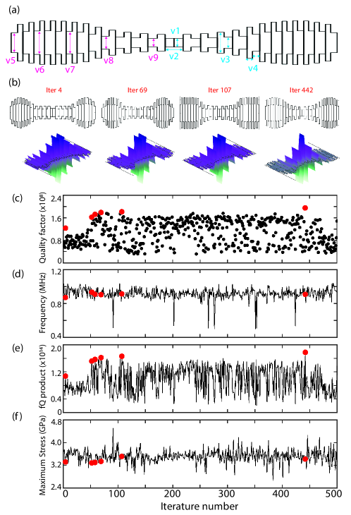
Bayesian optimization for ultra-high Q a-SiC nanostring made with a-SiCR2. The nanostring has a total length of 6 mm and the number of unit cells is fixed to 24. In the Bayesian optimization algorithm, the Q factor of the nanomechanical resonators is being optimized. 9 design parameters are setup for the optimization. The iteration steps are in total 500. Among the parameters, v1 is the defect width, constrained between 1 to 3 um; v2 is the defect length, constrained between 50 to 500 um; v3 is unitcell width ratio, constrained between 1:1.5 to 1:3; v4 is unitcell length ratio, constrained between 1:3 to 3:1; v5 to v9 are the widths of the unitcells’ thin parts, the width parameters defining the tapering shape, constrained between 1 to 3 um. Lengths of the unitcells was determined considering bandgap frequency matching condition, once the set of each unitcell’s width is defined [10]. One can find that the mode shapes are getting more and more confined from the clamping points to minimize the clamping loss. From the fifth optimized result (Iter 107) to the final optimized result (Iter 442), the geometry is changing from a uniformly corrugated design on the edge to a non-uniformly corrugated one, this interesting found might lead to interesting perspectives in designing the 1d PnC nanostring in the future. Interesting to note that the highest Q factor design doesn’t coincide with the design with the highest tensile stress.
Supporting Information (F): Thin a-SiC resonator
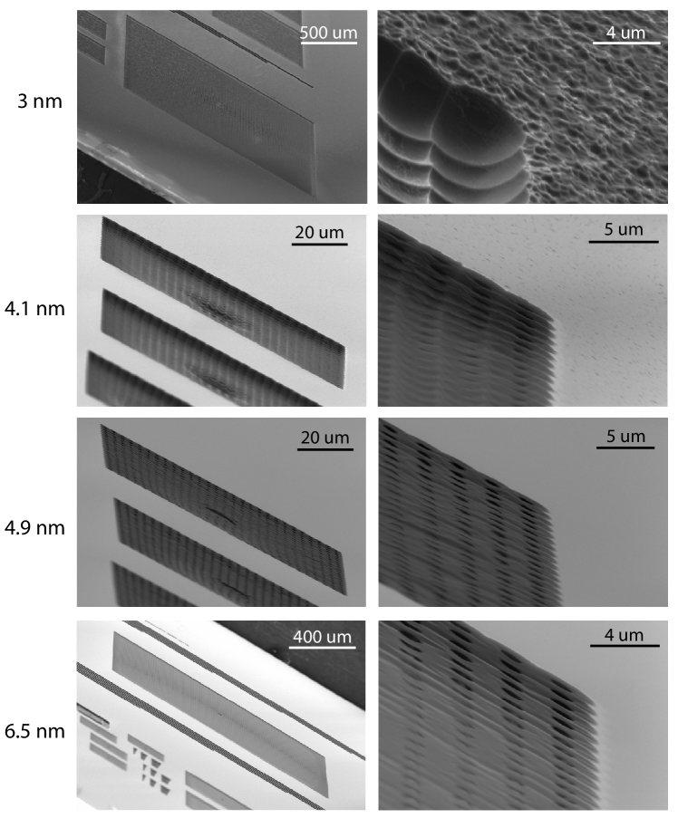
Both the force sensitivity and force responsivity of nanomechanical sensors are limited by the minimum thickness achievable for the continuous films. For thin film sensors with high intrinsic tensile stress , higher aspect-ratio (length/thickness) can increase the feasibility of higher Q factor, thus higher force sensitivity due to lower noise level; While for the ones with low film stress, thinner films lead to lower stiffness, therefore larger deflection under given forces, or higher force responsivity. Unlike 2D materials such as graphene, which use the bottom-up approach to construct ultra-thin suspended resonators (e.g. growing the thin film layer by layer atomically), engineerable thin films such as a-SiN and s-Si usually use the top-down approach to get ultra-thin resonators. As respectively shown in [102] and [14], in order to fabricate high-aspect-ratio (HAR) resonators with thicknesses down to 12nm SiN and 15nm (sSi) thin films, encapsulating layers are required to hold up as well as to protect the thin SiN and sSi structures, which complicate the fabrication processes and may even introduce contamination. Compared to the above materials commonly used for nanomechanics, a-SiC thin films can be fabricated into thinner resonators thanks to its superior chemical inertness. As shown previously, even with LPCVD, which is considered to deposit continuous and conformal films, cannot avoid pinholes on the films while depositing the first nanometers. In order to find out the minimum thickness achievale for a-SiC thin film, the ion beam etcher (SCIA Ion Mill 150) is used to thin down the thicker and more uniform GFR2 films down to the desire thickness. The ion beam etcher, compared to other techniques, such as reactive plasma etching, is preferred to get ultra-thin films down to sub-nanometer accuracy, with a physical sputtering process applicable to a wide range of materials called ion beam milling, which avoid surface contamination and local charge accumulation that might hinder to obtain the desired conformal thin film accurately. The GFE2 films with initial thickness 71nm are thinned down with a beam voltage of 120V (kinetic energy 120eV per ion) and an incident angle of 4 degrees sheering, resulting in an etch rate of 7 nm/h. By suspending resonators with polished film thicknesses from 3 to 6 nm on silicon substrate, we found that minimum continuous smooth LPCVD a-SiC GFR2 film achievable is between 4.1 and 4.9 nm. Worth to note that buckling patterns are observed on the trampoline resonator, due to the facts that: 1. the thinner and larger the resonator is, the smaller stress gradients in both in-plane and out-of-plane directions are required in order to keep the resonator flat [14, 23]; 2. the first several nanometers of the a-SiC film is with less tensile or even compressive stress due to defects at the material interface at the start of the deposition, which are also shown in [102, 15].
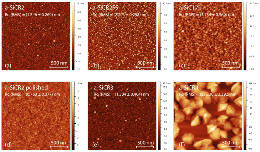
The surface topography of the a-SiCR2 thin film polished down to 3nm, is measured with AFM shown in SI. G(d), which is only half the RMS compared to the one prior to being polished.
Supporting Information (G): Surface topography of a-SiC thin films with Atomic force microscopy
Among all recipes, a-SiCR2 and a-SiCR3 have the lowest roughness. Yet one can still find large bright spots on a-SiCR3 films with the dark field image from the optical microscope, indicating that it is not as flat in a larger landscape. After polishing with the ion beam miller, a-SiCR2 with 3 nm is scanned, with only half the roughness compared to the one prior to polishing. Interesting to note that, with lower deposition pressure, a-SiC170 is rougher than a-SiCR2, which matches well with its lower intrinsic Q factor and lower fracture strength. The topography of a-SiCR4 is very rough, can be due to the re-crystallization of Si components in the thin film.
Supporting Information (H): Fabrication process
Low pressure chemical vapor deposition (LPCVD) non-stoichiometric a-SiC films were used in this paper, deposited with different gas flow ratios (GFR) between SiH2Cl2 and 5% C2H2 in H2 (GFR=2,3,4), at various deposition pressures (170/600 mTorr), and on both silicon and fused silica substrates (Table 1). The variation in deposition parameters allows us to systematically characterize the mechanical properties of LPCVD a-SiC. All a-SiC films were deposited at a temperature 760C for the same period of time (3 hours 47 minutes) to avoid film property differences caused by thermal effects and to ensure that the SiC films were composited of amorphous form instead of poly-crystalline form [73, 118].
After LPCVD a-SiC deposition, the wafers are diced into smaller chips. The chips are then exposed to electron beam lithograph to create desired patterns on the e-beam resist coated on top. Subsequently, these patterns are transferred into the a-SiC films using CHF3 anisotropic plasma etching. Next, the patterned chips are cleaned with dimethylformamide and Piranha solution, followed by the undercut of the silicon substrate or fused silica substrate using cryogenic SF6 isotropic plasma etching or vapor hydrofluoric acid. Finally, the designed a-SiC nanomechanical resonators are fabricated.
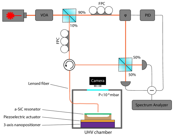
Supporting Information (I): Ringdown Measurement with Homodyne Detection
We use a balanced homodyne interferometer for performing ringdown experiments on a-SiC nanoemchanical resonators. As shown in Figure S11, the a-SiC nanomechanical resonator (green) on top on the substrate (brown) is placed in an ultra-high vacuum (UHV) chamber under a pressure lower than mbar. This avoids mechanical losses due to gas damping. Ringdown measurements are performed via a piezoelectric actuator which resonantly drives the corrugated nanostrings. After reaching maximal amplitude, the drive is stopped to observe the rate at which mechanical energy is dissipated from the nanostrings. The vibration amplitude of the resonator is measured optically with a fiber coupled infrared laser (1550 nm). The power of the laser is divided into two parts, 90% of it is used for interference reference (local oscillator), while the other 10% terminates with a lensed fiber shines on the resonator. The reflected light from the resonator then compares its phase to the one from the local oscillator using the balanced homodyne measurement setup, with which the amplitude of the resonator is measured.