[HTML]DB5800
Novel 2D vanadium sulphides: synthesis, atomic structure engineering and charge density waves
Abstract
Two new ultimately thin vanadium rich 2D materials based on VS2 are created via molecular beam epitaxy and investigated using scanning tunneling microscopy, X-ray photoemission spectroscopy and density-functional theory calculations. The controlled synthesis of stoichiometric single-layer VS2 or either of the two vanadium-rich materials is achieved by varying the sample coverage and the sulphur pressure during annealing. Through annealing of small stoichiometric single-layer VS2 islands without S pressure, S-vacancies spontaneously order in 1D arrays, giving rise to patterned adsorption. Via the comparison of density-functional theory calculations with scanning tunneling microscopy data, the atomic structure of the S-depleted phase, with a stoichiometry of V4S7, is determined. By depositing larger amounts of vanadium and sulphur, which are subsequently annealed in a S-rich atmosphere, self-intercalated ultimately thin V5S8-derived layers are obtained, which host V-layers between sheets of VS2. We provide atomic models for the thinnest V5S8-derived structures. Finally, we use scanning tunneling spectroscopy to investigate the charge density wave observed in the 2D V5S8-derived islands.
keywords:
transition metal dichalcogenides, VS2, V5S8, monolayer, charge density wave, layer dependence, atomic structure engineering, 2D materialsAtomic structure engineering of two-dimensional (2D) materials in order to tailor their electronic and chemical properties or to create novel phases has been on the forefront of recent research. Various methods to achieve this have been explored, like the introduction of point or line defects 1, 2, 3, creating horizontal or vertical heterostructures 4, 5, doping or gating 6, 7, 8, 9, as well as intercalation of native or foreign atoms between the layers 10, 11.
The creation of defects has been particularly successful in engineering transition metal dichalcogenides (TMDCs) 12. Chalcogen vacancies alone can be used to dope TMDCs 13, to develop or enhance a magnetic ground state 14, 15 or to gain increased surface reactivity 16, 17. Vacancies can be created by extrinsic means like electron-beam irradiation 13, 18, but can also spontaneously form under suitable conditions through thermal annealing 16, 15.
Since TMDCs are layered materials, they are also easily intercalated, with additional metal atoms placed between the TMDC sheets 11. Intercalated atomic layers have been used to enhance electronic conductivity, induce ferromagnetism, phase transitions or Ising superconductivity in TMDCs 19, 20, 21, 22, 23. While these intercalants have been used extensively to intercalate bulk TMDCs 10, 21, 22, 19, recently the focus has shifted to bilayer TMDC intercalation, being the thinnest intercalated material 24, 25, 20.
Among TMDCs, vanadium based compounds like VS2 have attracted substantial theoretical research interest due to their predicted electronically correlated and magnetic ground states when thinned down to a single layer 26, 27, 28, 29. However, due to the lack of a stable bulk polymorph 30, 31, VS2 is a particularly challenging material to synthesize as a few-layer system and it was a late addition of the single-layer TMDCs when it was synthesized on Au(111) 32 and on quasi-freestanding on Gr/Ir(111), where a charge density wave (CDW) was found 33. Owing to the wealth of experiments performed on VS2 and its sister compound VSe2 showing the absence of net magnetic moment in these materials, it is commonly accepted that the theoretically predicted ferromagnetic ground state 26, 27, 28, 29 is not realized in pristine single-layers of these materials 34, 15, 33.
In contrast, the stable compound V5S8 exhibits layer-dependent magnetism, which transforms with decreasing thickness from anti-ferromagnetic to ferromagnetic 35, 36, 37. These results have so far been limited to samples down to thickness since this compound has not yet been realized in its minimum thickness configuration of two VS2 layers sandwiching a V intercalation layer. Transport measurements of bulk V5S8 show no increase in the resistivity at low temperatures, suggesting it does not have a CDW 38, 39, though upon cooling down to , an anisotropic contraction of V-V bonds was observed using X-ray diffraction 40. Several studies also note that the magnetic moment of the intercalated V atoms can couple to the itinerant electrons in the VS2 sheets, leading to a Kondo effect 41, 42.
Here we explore two novel 2D vanadium-sulphide compounds, created using a two-step molecular beam epitaxy process. The synthesis consists of an initial growth step at room temperature and an annealing step at elevated temperature to enhance island shape and alignment. Depending on the amount of deposited material during growth, the temperature, and the S pressure during annealing, three materials of different V:S stoichiometry are obtained. Since V deposition always takes place in large S excess, the deposited amount is characterized through the amount of V deposited - the V atoms stay on the surface, while excess S evaporates. The unit used is monolayer (ML), which characterizes the V amount needed to grow a full single layer of stoichiometric VS2, i.e. an amount of V atoms per m2. The synthesis is performed in each case on the inert graphene (Gr)/Ir(111) substrate, which preserves the intrinsic properties of the material under investigation 43, 44.
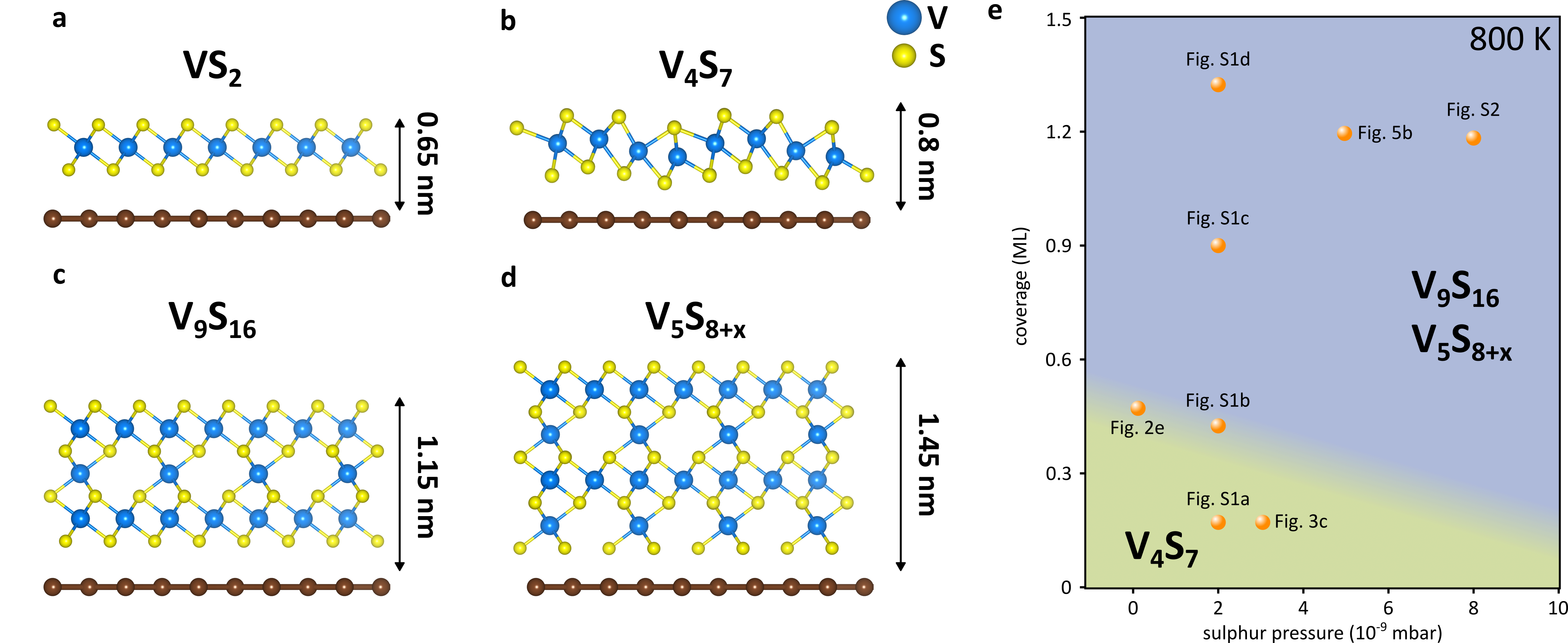
Single-layer islands of stoichiometric and phase pure VS2 are obtained when less than ML are deposited at room temperature and annealed to a temperature not exceeding 33. Under these conditions, the resulting single-layer VS2 is always present in the 1T phase, as depicted in Fig. 1a. When stoichiometric VS2 is exposed to higher annealing temperatures, it gradually transforms into V4S7, a process that is completed at an annealing temperature of . V4S7 has periodically arranged rows of S vacancies and an accompanying buckling of the lattice, see Fig. 1b. However, when the initial coverage during growth is larger, specifically when the islands resulting from the initial growth carry second layer islands of significant size, a different compound is formed upon annealing. It consists of layers of VS2 self-intercalated with V atoms in a pattern. The bulk stoichiometry of this phase would be V5S8, which has a NiAs structure with ordered V vacancies every second layer (leaving a quarter of the V atoms to form the ) 45. The V:S ratio of bulk V5S8 is a limit reached only when the number of layers goes to infinity. We obtain V5S8-derived islands of minimal thickness, consisting of two layers of VS2 with a layer of V atoms intercalated in the van der Waals (vdWs) gap between the layer. Consequently the stoichiometry is V9S16, see Fig. 1c. We also find evidence for the presence of a doubly intercalated structure. In that case, a second layer of V, passivated by S atoms, intercalated in the vdWs gap between the bottom VS2 sheet and Gr, as depicted in Fig. 1d. We denote this structure as V5S8+x, since the precise amount of S saturating the V is unknown. To show the different growth regimes in S pressure and coverage needed to obtain either the vacancy row structure V4S7 or the 2D derivatives of V5S8, a schematic representation is shown in Fig. 1e, wherein the structures obtained after room temperature growth and subsequent annealing at a temperature of are collected.
In this study, the materials shown schematically in Fig 1 are investigated using scanning tunneling microscopy (STM), X-ray photoemission spectroscopy (XPS) and density-functional theory (DFT) calculations. Furthermore, using low-temperature scanning tunneling spectroscopy (STS), a ( CDW is found in the 2D V5S8-derived islands, with a transition temperature below . An overview of our results is given in Table Novel 2D vanadium sulphides: synthesis, atomic structure engineering and charge density waves.
[HTML]eaa51f
| \rowcolor[HTML]eaa51f Growth parameters and properties of VSx compounds | ||||
| stoichiometry | VS2 | V4S7 | V9S16 | V5S8+x |
| coverage (ML) | ||||
| annealing temperature (K) | ||||
| annealing S pressure (mbar) | ||||
| purity | phase pure | phase pure | not phase pure, mixed with other V5S8-derived structures | not phase pure, dominant with excess V |
| CDW, | , K | none, none | (, K | |
| structure | T-phase TMDC | S-vacancy rows | - intercalation, V5S8-derived | |
| apparent height (nm) | 0.65 | 0.8 | 1.15 | 1.45 |
| figure | 2d | 2f | 5b | 6d |
1 Results
1.1 Creating 1D-patterned V4S7 from single-layer VS2
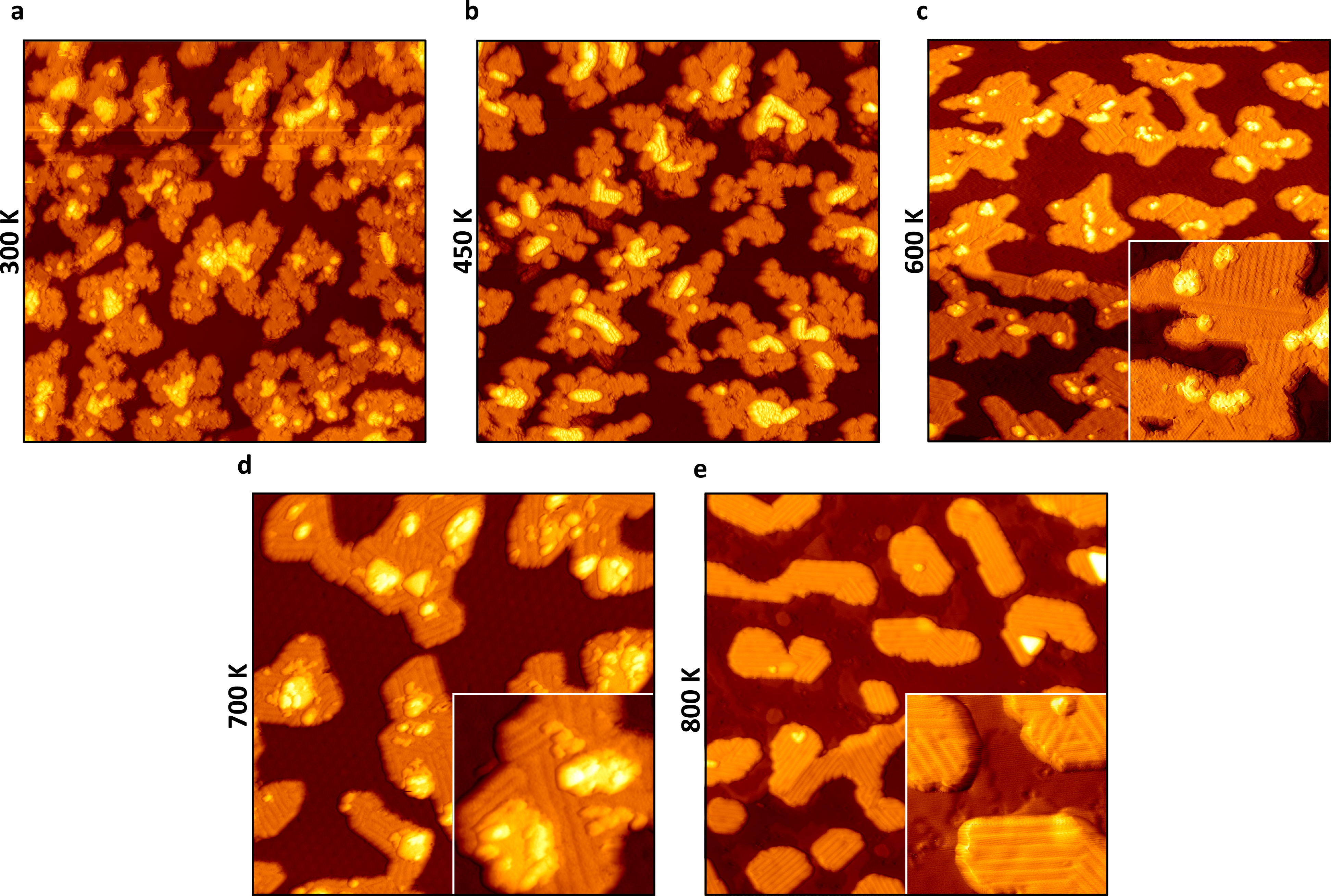
In Fig. 2a the sample topography directly after growth at room temperature is shown. Dendritic first layer islands of apparent height are visible, covered by small second layer islands. After annealing in vacuum to , see Fig. 2b, the single-layer islands are less rough, but dendritic shapes are still prevalent. After annealing to , in Fig. 2c, the islands are more compact with smoother edges. A superstructure, identified in previous work as a unidirectional charge density wave with an approximate unit cell of 33, covers all but the smallest regions of the islands. The CDW appears only after annealing to , as its formation requires sufficiently large islands of stoichiometric VS2. The instability of the CDW on small islands of VS2 has been documented in previous work 33.
Further annealing to , see Fig. 2d, leads to the dominant presence of a new type of striped superstructure (note that already at some stripes are present, compare Fig. 2c). The dark stripes have non-uniform spacing with a minimal width of and several domains of different orientations, as can be seen in the inset. After annealing to , in Fig. 2e, the VS2 islands are elongated but compact and display a well-ordered pattern of stripes. The stripes are generally aligned with the island edges and exhibit only three domains, rotated by . The islands have an altered apparent height of (see Note 3 of the Supporting Information (SI) for line profiles of the relevant topographies). The area of the islands has decreased - correspondingly, patches of what are presumably S and V atoms intercalated under the Gr are visible. Annealing beyond leads to the formation of higher structures, discussed below, and elongated crystallites which are not studied in the present manuscript, see Note 4 of the SI.
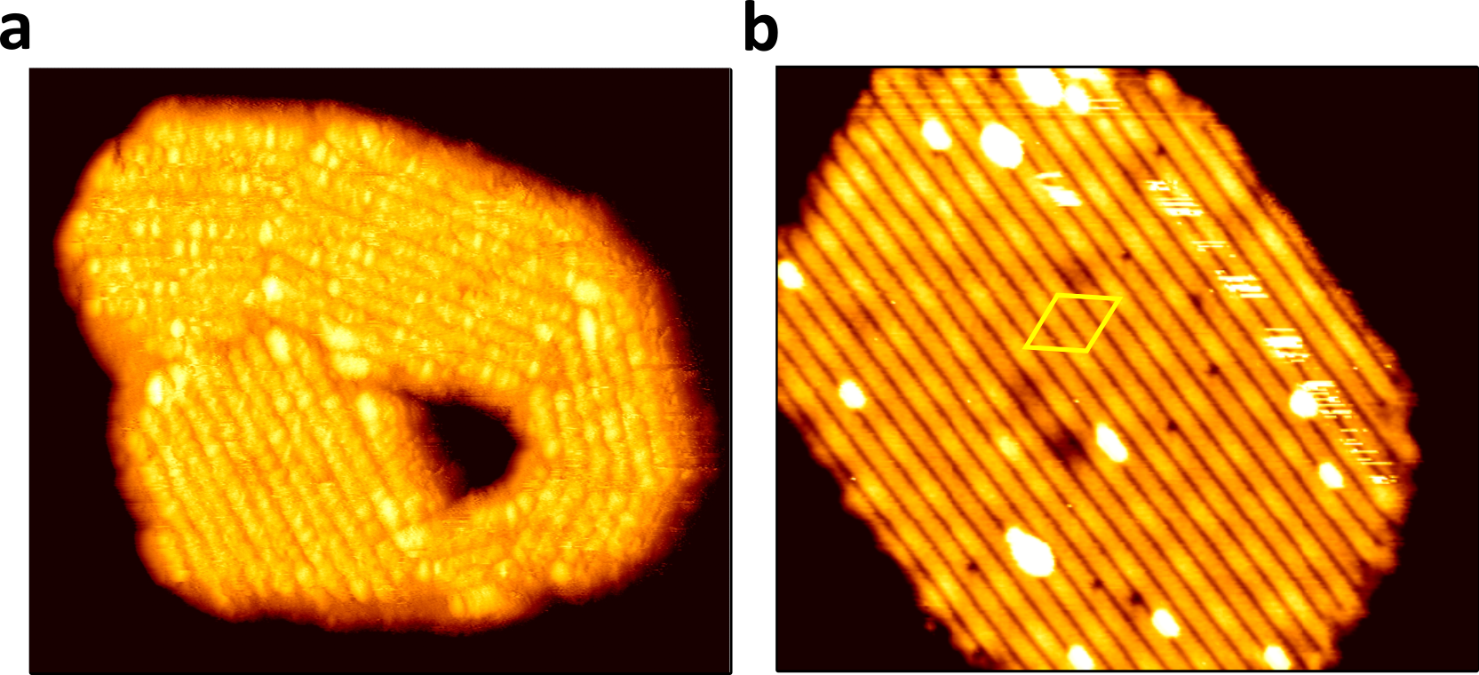
Focussing on the stripe superstructure, Fig. 3a shows the result of annealing the stripes to in a moderate sulphur background of = . Bright stripes of adsorbates are present on the island, with a spacing corresponding to the periodicity of the superstructure. Subsequent annealing largely removes the adsorbates uncovering the superstructure again, as shown in Fig. 3b. Only some bright adsorbate clusters are left. The moiré of Gr/Ir(111) (marked with a yellow rhombus) becomes apparent again after annealing.
We interpret the situation as follows: upon cooldown from the annealing step, residual S, which is hard to pump out, adheres to the islands. The subsequent brief heating in clean UHV causes desorption of these adsorbed S atoms. Irrespective of the details, the observations imply a modulated reactivity of the stripe superstructure. Note that for stoichiometric VS2 islands such structured adsorption was never observed. Note also the reconstructed island edges in Fig. 3b, with the the stripes causing kinked edges in segments parallel and orthogonal to them. The stripe superstructure being imprinted on the step edge highlights that the structure is not of electronic but of structural origin.
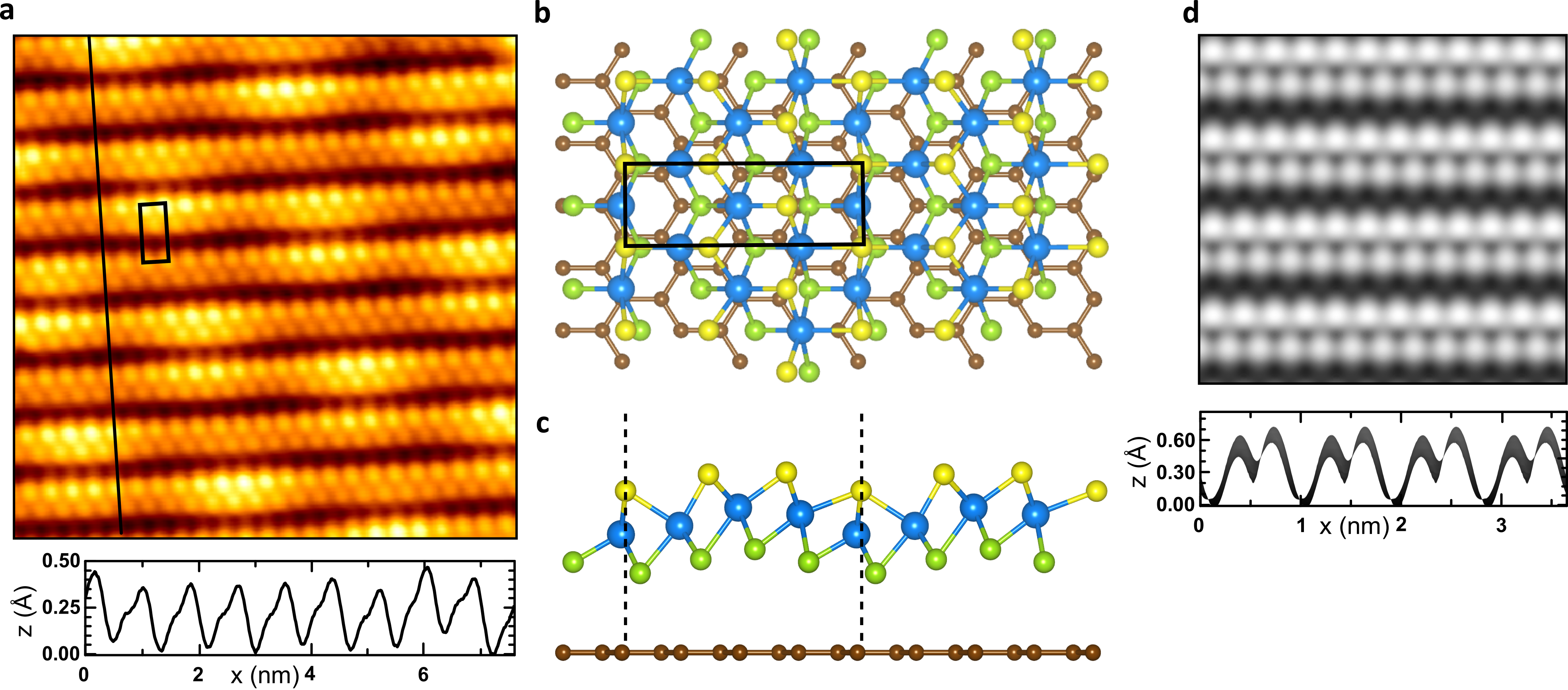
Turning to the atomic structure of the stripes, Fig. 4a shows an atomically resolved image of the surface of a striped single-layer island. The rectangular unit cell is shown as a black box. Its dimensions are along its short axis and along its long axis. The line profile along the black line shows an apparent height corrugation of about . Depending on the tunneling conditions the apparent height varied in the range from to . The STM contrast allows identification of two rows of atoms (presumably S atoms separated by grooves with a faint substructure.)
Assuming the superstructure to result from S desorption and given the rectangular symmetry of the unit cell with a S atom at each corner of the unit cell, it would be compatible with a VS2 lattice from which either every second or every fourth row of S desorbed. If this would occur without any other changes in the bonding distances of the V and lower S layer, one would expect a periodicity of either or normal to the removed rows. While the periodicity resulting from the removal of every second S row is inconsistent with the measured unit cell dimension, the somewhat larger unit cell size derived from our assumption of every fourth S row removed could be rationalized by a bond order – bond length argument: the remaining atoms strengthen their bonds and consequently shorten them.
A model involving the removal of every fourth row was also proposed for a similar sized unit cell with same symmetry by Liu et al. 16 for the sister compound VSe2. They observed a striped phase after annealing monolayer VSe2 grown on graphite.
To clarify the situation we conducted DFT calculations confining VS2 to the size of the experimental unit cell. We placed the VS2 layer on Gr and removed every fourth top layer S row. After relaxation, the structure shown in Fig. 4b,c was obtained. The nominal composition of the comound is V4S7. The removal of the S atom row has led to a buckling of the structure and changed the coordination of one of the remaining rows of S atoms from threefold to fourfold. The simulated STM image shown in Fig. 4d, using precisely the same sample bias of -0.5 V as in the experiment, shows striking agreement with the experimental topograph of Fig. 4a. The predicted corrugation of the structure of matches reasonably well with experiment, as does the asymmetry of the profile.
Giving up the constraint of an initially intact VS2 layer with just S rows removed, alternative models can be considered. If an additional VS2 unit is removed per cell, the compound V3S5 is formed by bond reorganisation. Simulated STM topographs reproduce the experimental STM contrast reasonably well (compare Note 5 of the SI). However, the corrugation of the resulting structure is well above , at variance with experiment. Its formation would furthermore involve bond breaking and either loss V or expansion of islands, which are also considered to be unlikely. A model similar to this scenario was proposed by Chua et al. 15 to explain a striped phase after annealing of monolayer VSe2 on MoS2. However, their unit cell was substantially larger and of different symmetry than the S compound discussed here.
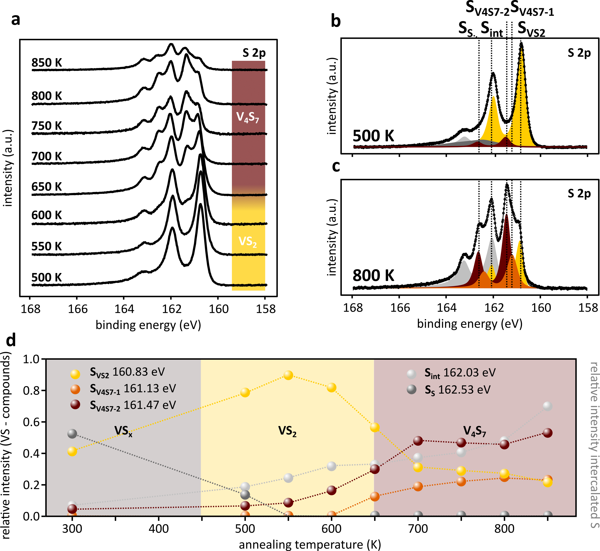
In order to obtain additional information about the effect of annealing stoichiometric VS2, we performed high-resolution X-ray photoemission spectroscopy (XPS) of the S 2p core level. Fig. 5a shows the S 2p core-level spectra obtained for samples with increasing annealing temperatures in the absence of S pressure from bottom to top. Spin-orbit coupling of the S 2p level gives rise to an S 2p3/2 and S 2p1/2 doublet separated by . At only a single S 2p doublet is visible, with peaks at and . As the annealing temperature is increased, more doublets become pronounced. In particular, the S 2p peak intensities shift toward higher binding energies. At the highest annealing temperature of the total intensity of the signal is significantly reduced.
Fitting the XPS spectra across the whole range of annealing temperatures requires five doublets, which will be discussed by reference to the lower binding energy 2p3/2 peak of the doublet. In Fig. 5b, a single component (, yellow) dominates the spectrum, denoted S. In contrast, the spectrum in Fig. 5c is made up of multiple doublets of similar intensity. Crucially, two new doublets close to the original yellow component are present at , which we denote S (, orange) and S ((, brown). Comparison to the spectrum furthermore reveals that the dark grey () component S has disappeared, whereas the silver () component S is still present and has larger relative intensity.
From STM images we know that at or below , mainly unperturbed (though defective) single-layer VS2 islands are present (compare Fig. 2a,b,c). We therefore assign S to stoichiometric VS2. S, which disappears rapidly when the sample is heated up from room temperature, we assign to sulphur species which react or desorb upon annealing. S, on the other hand, can be straightforwardly assigned to S atoms intercalated between Gr and Ir(111) 46. The presence of intercalated S atoms is inferred from STM images (see Note 6 of the SI) and low-energy electron diffraction (LEED), an example of which is shown in Fig. 7. The assignment is further based on the presence of this peak at the same location for all samples investigated in this study. Its high binding energy furthermore sets it apart from the peaks intrinstic to the vanadium sulphide compound. S and S finally, are related to the formation of the striped vacancy row V4S7 observed in STM, as these components are present in significant intensity only at higher annealing temperatures.
Plotting the relative intensities of all components against the annealing temperature in Fig. 5d, we can broadly distinguish three stages. At , stoichiometric VS2 is coexisting with unreacted sulphur (compare Fig. 2a and Note 7 of the SI). Upon annealing to , the sulphur desorbs from the surface, leaving a sample consisting mainly of stoichiometric VS2, with about of the vanadium sulphide intensity stemming from the S component. Above , the sample undergoes a transition to V4S7, with S and S becoming prominent with a ratio that tends to . Because of this ratio, we assign S to the two almost equivalent, threefold coordinated S atom rows in the DFT calculation of Fig 4b,c, and S to the other S atom row, which has a fourfold coordination, see Note 8 of the SI. While S is reduced in intensity and shifts to a slightly higher binding energy by when the sample is annealed, it remains present up to , when the sample surface uniformly exhibits the striped superstructure. We infer that this signal stems from the bottom S atoms, which are in a chemical environment not too different to that of pristine VS2. At higher annealing temperatures, the S detached from VS2 intercalates below Gr, which can be seen in Fig. 2e, leading to the strong increase in the relative intensity of the S component.
In conclusion, we interpret V4S7 to emerge gradually with increasing annealing temperature through loss of sulphur from the initial VS2 islands and an accompanying reconstruction of the atomic lattice (compare Figs. 2c-e). At about , the density of the vacancy rows has reached a saturation, resulting in uniform V4S7 characterized by every fourth sulphur top layer row missing. The XPS spectra, which show the appearance of new S 2p doublets at considerably higher binding energies, support this interpretation. In particular, two new S 2p components indicate that most of the top layer S atoms are in a different chemical environment compared to pristine VS2, which makes a different stoichiometry likely. The loss in S is accompanied with a substantial lattice reconstruction, also consistent with the reshaping of the islands, which reflect the vacancy row periodicity. In contrast, no significant changes are observed in the V 2p XP spectra, see Note 9 of the SI.
The observation of a striped sulphur depleted phase after annealing of a monolayer of VS2 or VSe2 appears to be a common feature of these materials. However, the precise structure that is obtained depends on the substrate. Annealing of VS2 on graphite results in V4Se7, as observed by Liu et al. 16; similarly, annealing of VS2 on graphene results in V4S7, as observed by us. Despite the difference in the chalcogen, the same stoichiometry and very similar structures with a rectangular unit cell and an orthorhombic 2D Bravais lattice are formed. Although annealing of VSe2 on MoS2 as done by Chua et al. 15 leads to the same stoichiometry V4Se7, the unit cell is oblique and the symmetry is that of a monoclinic 2D Bravais lattice. Finally, annealing of monolayer VS2 on Au(111), as conducted by Arnold et al. 32 and Kamber et al. 47, results in a more S-depleted stoichiometry of V2S3, which in addition has a quite different internal structure of the cell. It would display single rows of S atoms rather than the double rows as observed experimentally and simulated by DFT (compare Fig. 4).
The formation of chalcogen vacancy rows or line defects due to annealing, electron or laser beam irradiation seems furthermore a general feature in TMDCs 48, 49, 50, 51. In the case of single-layer VSe2, annealing-induced Se-vacancy rows were used to lift the spin-frustration of the material, leading to room-temperature ferromagnetism 15. Since the CDW ground state responsible for the magnetic frustration 52 is very similar in both stoichiometric single-layers of VS2 and VSe2, it would be of great interest to track the effect of annealing VS2 on its magnetic properties. In contrast to VSe2 however, where it is possible to transform the patterned state back to stoichiometric VSe2 via low-temperature annealing after deposition of Se atoms 16, 15, low-temperature annealing in sulphur vapour did not recreate stoichiometric VS2 from V4S7. Depending on the coverage of the sample, either adsorbed S atoms on top of the patterned material were observed, depicted in Fig. 4d, or - in the case of larger coverage - higher structures were obtained, which will be discussed below.
1.2 Self-intercalation of V atoms in multilayer VS2
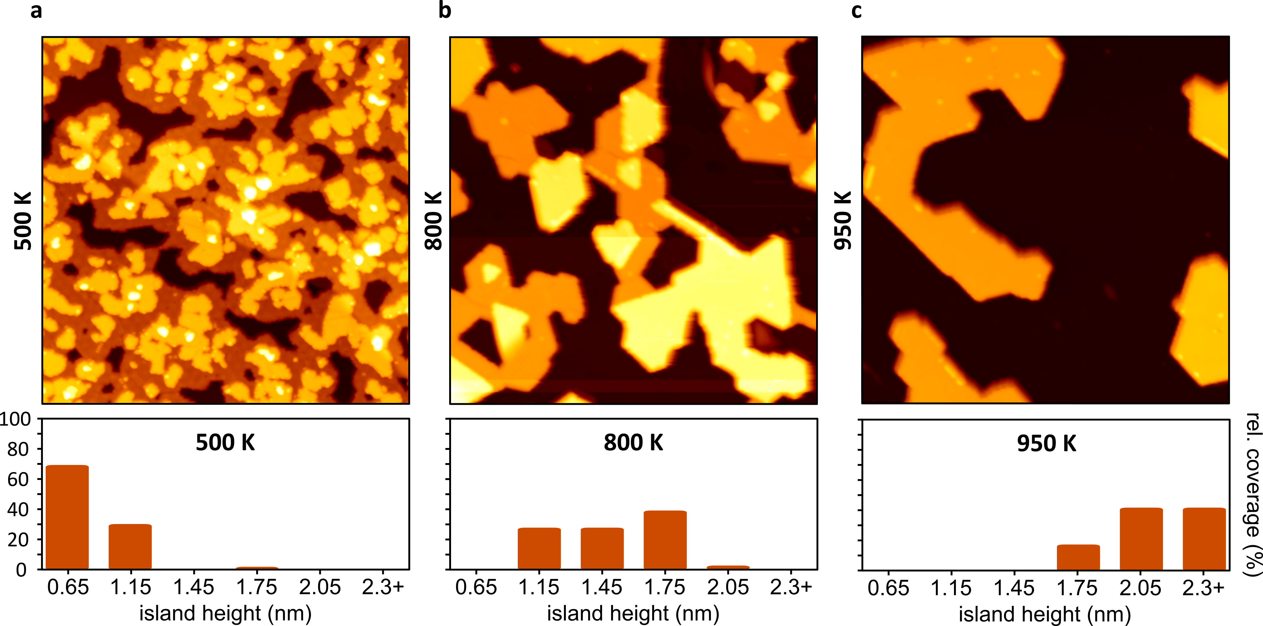
Instead of single-layer VS2 or V4S7, we can selectively grow a new 2D material by changing the growth conditions to favor higher structures. Already during growth at multilayer structures form (see Fig. 2a). As we deposit more material, a substantial fraction of the material will grow on top of single-layer VS2. When we then anneal in S-rich environment to about , structures with several height levels are created, which do not manifest S vacancies in their top layer.
In Fig. 6a-c the evolution of such a sample is depicted. After annealing ML of VSx to , the apparent height distribution shows the apparent height characteristic for single-layer VS2, a significant area fraction of height and some small areas of apparent height, as shown in Fig. 6a. Annealing the sample to leads to a transformation of island shapes and apparent heights, shown in Fig. 6b. The island edges are straight, largely aligned to the dense packed directions of Gr. In addition, two new island apparent heights appear ( and ), both offset from the higher islands already present at . The lowest islands are now high. No single-layer VS2 is present on the surface. While the different islands are generally sharply demarcated by step edges from one another, continuous transitions between them are also observed, like in the bottom left of Fig. 6b. These transitions will be discussed below. When the sample is further annealed to , as shown in Fig. 6c, only islands with apparent heights of and up are observed. We thus find that as the annealing temperature increases, the island density goes down, while the average apparent island height increases, with island heights separated by . The resulting sample cannot be understood as multilayer VS2, since the height of each VS2 layer is . We therefore refer to these samples as multiheight VSx. Our investigation will focus on the lower two levels of and apparent height, which will be identified as 2D derivates of V5S8.
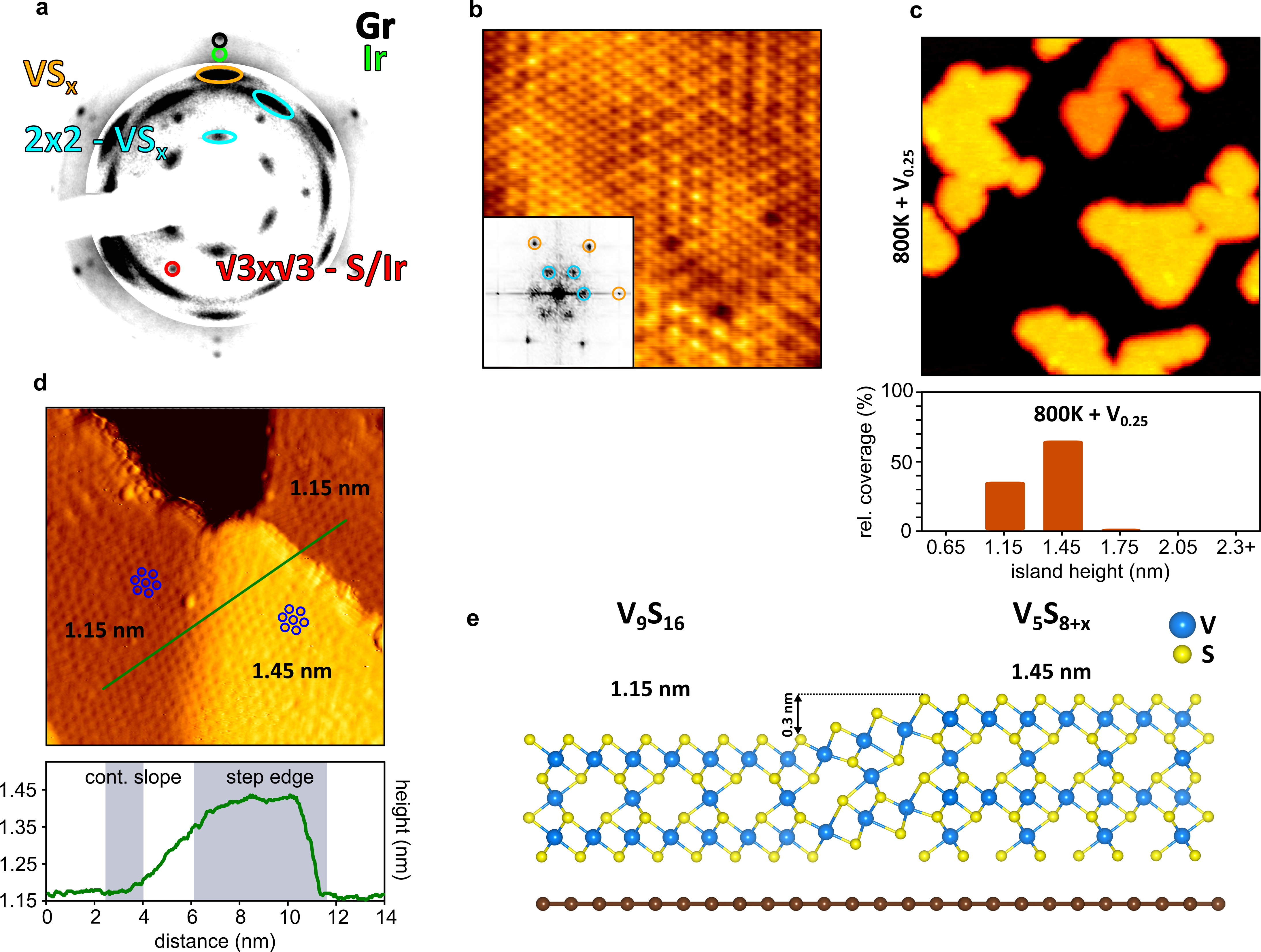
In the LEED pattern of the multiheight sample annealed at , where the apparent minimum island height is , we find multiple ordered structures, see Fig. 7a. The Gr (black circle) and iridium (green circle) first order spots are visible, surrounded by hardly visible satellite spots from their moiré. Closer to the center, sharp spots with respect to Ir [] are present, which stem from S intercalation under Gr. The VSx spots (orange ellipses) are elongated, indicating a small epitaxial spread in orientation angles, which sets them apart from the perfectly oriented spots of the substrate. Besides the first order VSx spots, two other sets of spots with the same elongation are visible, which are identified as first and second order spots of a superstructure with respect to VSx. The first order spots indicate a hexagonal symmetry with a lattice parameter of . This is close to the lattice parameter of stoichiometric VS2 () 53, 33. However, the strong reflections are characteristic of V5S8, a material of monoclinic symmetry which can be understood as a bulk crystal consisting of sheets of VS2 with a layer of V atoms in between 45.
An atomically resolved STM topograph, taken at room temperature, of a high island after annealing to , depicted in Fig. 7b, shows that the material has preserved its hexagonal symmetry on the surface - as expected from the LEED pattern. At room temperature and under favorable imaging conditions, along with the atomic lattice, a superstructure is visible. The superstructure is slightly disordered. This is evident also in the fast Fourier transform (FFT) shown in the inset of Fig. 7b, where the spots (green circles) are broader than the atomic lattice spots (yellow circles). The presence of a superstructure in STM is consistent with a intercalation layer, as expected for V5S8. The fact that it is hard to image and not present on all atomic resolution topographs obtained indicates that the does not originate from the top layer, again as expected for an intercalation layer in a V5S8-derived structure.
To confirm that it is straightforward to self-intercalate V into existing layers, we evaporated additional V atoms on an already grown VSx sample annealed to . Prior to V deposition, the sample was comparable to the sample shown in Fig. 6a, with uncovered single-layer VS2 and some islands of apparent height. The evaporation was performed in UHV, with no additional S added. After deposition, the sample was annealed to in UHV - so again without the addition of any S. The result is shown in Fig. 7c. Compared to Fig. 6b, which was annealed to the same temperature, the ratio of islands to islands has increased and little to no thicker layers have formed. Crucially, no V atoms or clusters are present on top of the islands or the Gr. The V atoms have been incorporated in the islands, changing their stoichiometry. In the LEED of this sample, a clear signal can be distinguished, consistent with our interpretation of a intercalation structure, see Note 10 of the SI.
No structural differences exist between the surfaces of the and islands. On the contrary, a continuous transition from one island type to the other is possible, as evinced in Fig. 7d. In the image, an island of apparent height is seen to continuously transform into the island of on the right hand side, while a step edge separates it from the island in the upper left, as seen in the line profile below Fig. 7d. Because of this continuity, we conclude that the structure of the islands is essentially the same.
The thinnest possible form of V5S8 consists of two layers of VS2 intercalated by a single sheet of V atoms and has a stoichiometry of V9S16, see Fig. 1c. The second thinnest 2D V5S8-derivative would then have a second intercalation layer under the lower S atoms. With these structures in mind, we give an atomic model that explains the continuity in Fig. 7e. Since V atoms below the island would be highly reactive, we presume that they are passivated by S atoms. This additional layer of V and S accounts for the apparent height difference between the islands, see in Fig. 7e. The stoichiometry of the thicker island, with two V intercalation layers, is dubbed V5S8-x, since the exact configuration of the bottom S atoms is not known. 2p3/2 and S 2p1/2
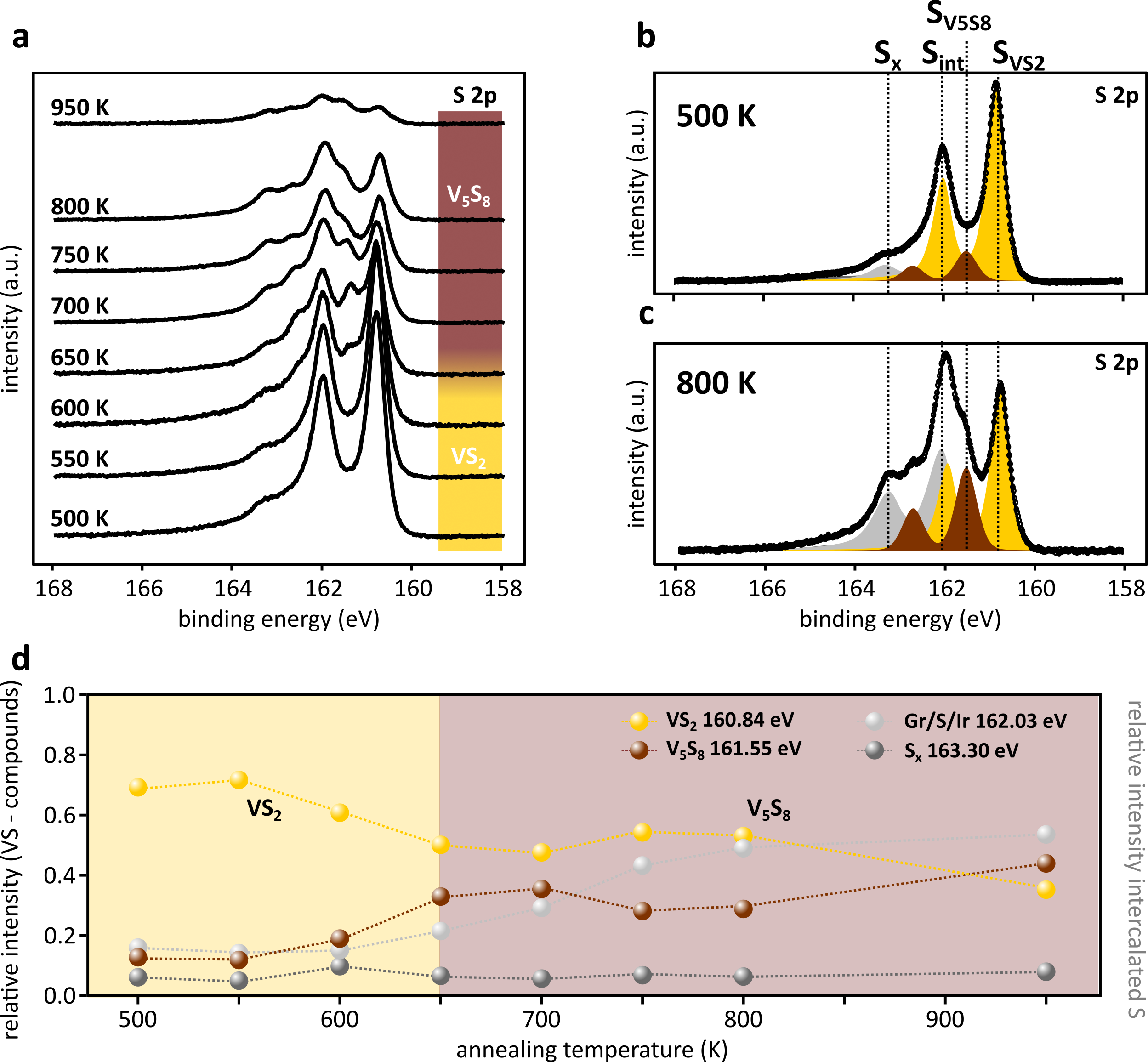
Using XPS we investigated the S2p core level of VSx at different temperatures during an annealing experiment in a S-rich atmosphere corresponding to the STM sequence in Fig. 6. The result is displayed in Fig. 8a. After annealing to , the S doublet at and is most prominent in the spectrum, indicating the dominant presence of stoichiometric VS2, see Fig. 8b. When the annealing temperature is increased, S decreases in intensity and a new doublet S appears at the higher binding energy of (brown in Fig. 8c). The total intensity of the signal is reduced significantly. However, unlike the annealing sequence in Fig. 5, where a small coverage of VS2 was annealed without S pressure, the S component in Fig. 8 remains dominant up to . When we fit the spectra, using the same fitting parameters for S and S as for the fits of Fig. 5, we find that we obtain a reliable fit for a total of four peaks. Besides S, we added a minor dark grey component S located at , hardly visible in the spectra and of unkown origin. Additional XP spectra of the sample with extra V atoms, shown in Fig. 7c, can be found in Note 11 of the SI.
Tracking the relative intensities of all components in Fig. 8d, it becomes apparent that S is already present at the lowest investigated temperature and grows at the expense of S, with an onset for the growth between . S remains of equal low intensity throughout the annealing process, while S grows as the annealing temperature is increased.
We interpret the two characteristic components in V5S8-derived islands to stem from S atoms in two different chemical environments. S atoms bound only to 3 V neighbours as in VS2 give rise to the S component, which undergoes a small shift on the order of towards lower binding energies upon intercalation, while S atoms next to the V intercalation layer, being bound to more than 3 V, give rise to the S component. Although the superstructure in STM and LEED alone could stem from a lattice distortion, the strong shift () in the binding energy of the S atoms from the S to the S doublet signals a more significant change in the chemical environment of the atoms. A similar shift to higher binding energy was observed in self-intercalated bilayers of VSe2 in Ref. 54, where it was associated with a change in the electrostatic energy at the Se sites coordinated to more than 3 V atoms. Analogous to the XP spectra of V5S8, again no significant changes are observed in the V 2p XP spectra, see Note 12 of the SI.
Islands thicker than are most likely also V5S8-derived. Consquently, the number of S atoms bordering -V planes increases upon annealing, causing the S component to rise, while the number of surface S atoms decreases, leading to the decrease of the S component and the observed shift in relative ratio between the components. Since XPS is a surface sensitive technique, the S component stemming from the top S atoms will generally outweigh XPS signals of S atoms deeper in the islands, which explains the dominant presence of S even when most islands have one or more intercalation layers. We also cannot exclude the presence of (unintercalated/partially intercalated) vdWs gaps in the thicker islands. Their precise analysis lies beyond the scope of the manuscript.
Concerning the other components, the comparatively small increase in the relative intensity of S, compared to the increase of the same component in the XPS of single-layer VS2, is probably due to the presence of S-intercalation already after annealing at , since all annealing steps were performed in a S-rich environment (note the high intensity of the S intercalation spots in the LEED of Fig. 7a). The increase in the intensity of S is thus a measure of the reduced surface area of the islands, exposing more of the Gr. The S component has little weight and its origin cannot be uniquely determined. It could stem from adsorbed S, since it has a similarly high binding energy as the S component in the monolayer.
To summarize at this point, we interpret the islands formed when annealing a large ( ML) deposited amount of VSx in a S background pressure as being V5S8-derived. This is indicated by the simultaneous presence of a superstructure in LEED and STM and the new S component in the S 2p XPS spectra, with a binding energy higher than S. We are able to create a more pure minimal-thickness V5S8 sample via the evaporation of extra V atoms on a multiheight sample annealed to , and then annealing it to , as depicted in Fig. 7c.
We note finally that in similar fashion V5Se8 was previously procured from seed layers of VSe2 during thin film growth 55, or by increasing the substrate temperature during growth or annealing of single-layer VSe2 56, 57. In a similar vein, the chemical vapor deposition growth of VS2 nanosheets generally leads to the simultaneous presence of VS2 and V5S8 58, 59. In each case, the small differences in formation energy between the self-intercalated material and the TMDC are emphasized. Here, we showed that providing extra V atoms after an initial growth step can help to favor one phase over the other and enables one to grow phase pure ultrathin V5S8-derived material down to the minimal thickness of . These minimal thickness islands with a stoichiometry of V9S16 can be considered as single layers of a new 2D material.
1.3 ( CDW in ultimately thin V5S8-derived islands
When we cool down the multiheight sample, we find that the islands of and apparent height undergo a structural phase transition. In both island types, a pronounced superstructure with a periodicity of is observed in topography at temperatures . This superstructure can already be seen clearly in Fig. 7d, where the ( superstructure maxima are encircled in blue. It coexists with the CDW in the monolayer, see Note 13 of the SI.
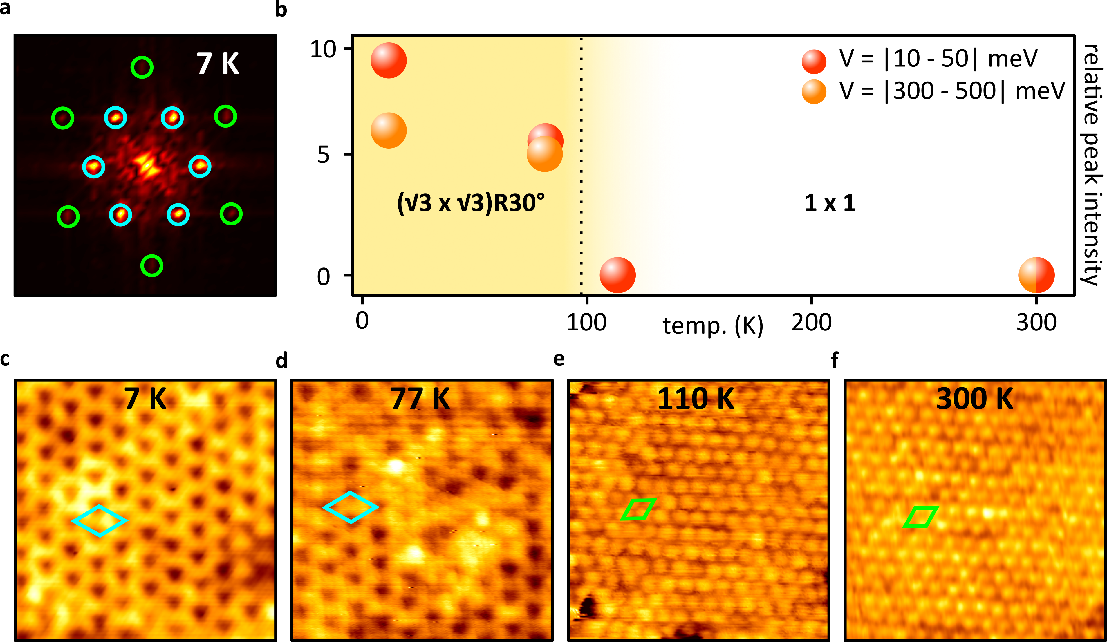
Upon heating the sample from back to room temperature, the ( superstructure vanishes and the atomic lattice becomes visible. As a measure of the strength of the superstructure, we take the relative peak intensity of the Bragg peaks with respect to that of the ( peaks 60. In the FFT shown in Fig 9a, these are encircled in green and cyan, respectively. Plotting the relative intensities for FFTs obtained at different temperatures in Fig 9b, the ( can be seen to disappear between and (see Note 14 of the SI for all topographies and FFTs). Some representative topographies are shown Fig 9c-f, which make clear that the atomic lattice is recovered at . From the strong temperature dependence of the ( superstructure, we conclude that it is likely a charge density wave. This CDW is not to be confused with the one that develops in single-layer VS2, which is unidirectional and has a much higher transition temperature 33, see Table Novel 2D vanadium sulphides: synthesis, atomic structure engineering and charge density waves for the differences.
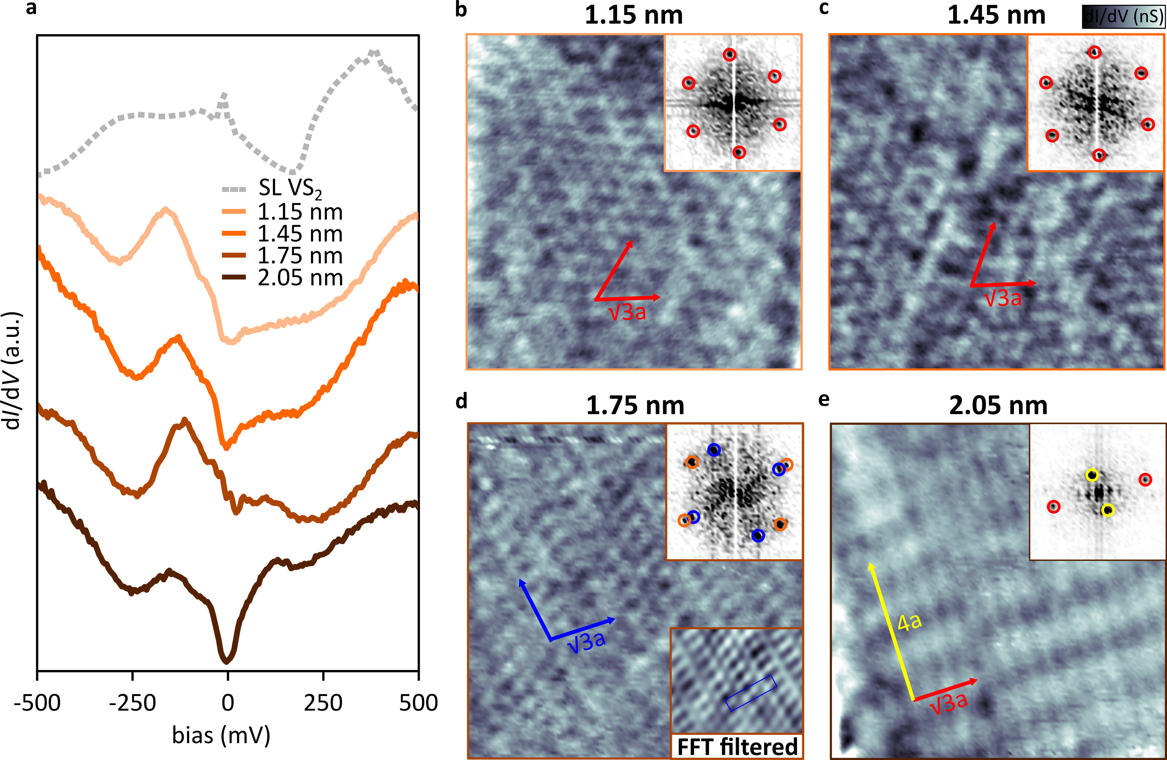
Finally, turning towards the electronic structure of the multiheight islands, we see in Fig. 10a that, in contrast to ML VS2, which hosts a CDW with a full gap above the Fermi level 33, d/d spectra taken on the thinnest V5S8-derived islands ( and ) show a partial gap around , while a large density of states (DOS) peak is observed below . Comparing d/d spectra of islands of different apparent heights, taken with the same tip, we see essentially no differences between islands of and apparent height, which is in line with the fact that both have the same ( CDW.
Islands of , however, have a spectrum with no clear gap around and instead a depression around . At apparent height, yet another spectrum is obtained, which lacks the large DOS below that characterizes the other spectra and instead displays a more symmetric distribution of states on either side of . While it is tempting to correlate the presence of a gap at the Fermi level with the CDW, a more thorough investigation, backed up by DFT calculations is necessary to fully resolve this issue. Gaps at the Fermi level have also been argued to arise due to e.g. inelastic tunnelling effects 61, 62, whereas CDWs do not always lead to Fermi-level gaps which can be resolved with STM 33. In this case, temperature-resolved ARPES data could give more insight into the mechanism of CDW formation.
d/d maps taken on the islands at , as shown in Fig. 10b-e, reveal that these differences in electronic structure are accompanied by the presence of different CDWs. Note that all maps shown are taken at the same bias voltage , with the same tip, see Note 15 of the SI for an overview STM image showing all investigated islands. While the two lower islands both show the aforementioned (, the lattice symmetry is broken in the higher islands, which exhibit striped superstructures. Upon closer inspection, the superstructure can be understood as a ( structure, together with dimerization along one of the high-symmetry directions of the lattice, which is highlighted in the inset Figs. 10d. The dimerization breaks the symmetry and leads to a distortion of the FFT spots. The superstructure of the island shown in Fig. 10e, on the other hand, can be readily decomposed into a and a component, which are orthogonal to one another.
These differences illustrate the complexity of the system and would require a further and more detailed investigation. However, regardless of the actual composition, this variety of superstructures of slightly differing thickness and stoichiometry is striking. It underscores both the ubiquity of CDWs in low-dimensional vanadium chalcogenides and the metastability of any particular periodicity. It can be seen as an analogue to the case of VSe2, which hosts a plentitude of CDW phases, depending on its substrate and the number of layers 63, 64, 65, 66, 67.
With respect to V5S8 in particular, the fact that it hosts a CDW when thinned down to its 2D limit could shed new light on the layer-dependence of its magnetism, which changes from anti-ferromagnetic to ferromagnetic when thinned down to 35, 36, 37. Since bulk V5S8 is not known to have a CDW, the interplay between the formation of the ( CDW and the magnetic structure would be a compelling subject for further study.
2 Conclusion
In conclusion, we have grown and investigated two novel 2D vanadium-sulphur compounds: V4S7 and V9S16, the latter being the thinnest possible V5S8-derived material.
V4S7 is created from ML VS2 by the formation of S-defects through annealing without additional sulphur vapor. At an annealing temperature of , the S defects have spontaneously ordered into a homogeneous array of 1D trenches. We have shown that this 1D pattern templates S adsorption and speculate that also other adsorbates can be templated through the vacancy row pattern. Based on size and symmetry of the experimental unit cell, ab-initio DFT calculations were able to provide a stable structure model for V4S7, which is fully consistent with the STM data.
V5S8-derived islands are obtained automatically when a larger coverage ( ML) of VSx is grown. Second layer nucleation on top of single-layer VS2 does not occur as bilayer VS2; instead, V atoms intercalate between VS2 layers in a pattern and form V9S16. Annealing a mixture of single-layer VS2 and V9S16 in a S-rich atmosphere to leads to further self-intercalation of V atoms and the creation of a variety of structures of different apparent height. However, when additional V atoms are supplied after growth, phase-pure minimal thickness V5S8-derived material is obtained as a mixture of V9S16 of thickness and V5S8+x with thickness. Using low-temperature STM, these 2D V5S8-derived structures were shown to undergo a CDW transition to a ( phase, which develops below , whereas the thicker islands were found to exhibit different superstructures, presumably all of CDW origin.
Our findings provide a recipe for the growth of two new single-layer vanadium compounds. Given the thickness dependent magnetic and electronic properties of V5S8, having access to its 2D form is of particular interest for the further development of 2D magnetic materials.
3 Methods
The experiments were conducted in five ultra high vacuum systems (base pressure in the low range). Three systems were equipped with sample preparation facilities, scanning tunneling microscopy (STM) - operating at base temperatures given in the figure captions - and low energy electron diffraction (LEED). The fourth system was the FlexPES beamline endstation preparation chamber at MAX IV, Laboratory Lund, Sweden. There the samples were grown following the same recipes as in the STM system and sample quality was checked by LEED. The fifth system was an STM-only system, to which samples from FlexPES were transferred with a vacuum suitcase and then measured by STM at room temperature and .
Ir(111) was cleaned by cycles of noble gas sputtering ( Xe+ at with respect to the surface normal or with Ar+ at normal incidence) and annealing to . A closed monolayer of single-crystalline Gr on Ir(111) is grown by room temperature exposure of Ir(111) to ethylene until saturation, subsequent annealing to and followed by exposure to ethylene at 68.
The synthesis of vanadium sulphides on Gr/Ir(111) is based on a two-step molecular beam epitaxy approach introduced in detail in Ref. 43 for MoS2. In the first step, the sample is held at room temperature and V is evaporated at a rate of atoms into a sulphur background pressure of built up by thermal decomposition of pyrite inside a Knudsen cell. In a second step, the sample is annealed to with or without S pressure.
The XPS experiments were conducted at the FlexPES beamline at MAX IV Laboratory, Lund, Sweden 69. The S 2p core levels were measured with a photon energy of . The measurements were conducted at room temperature with a spot size of . The spectra for each sample were fitted simultaneously for all temperatures with pseudo-Voight functions. The width, skew and ratio of Gaussian to Lorentzian contributions were fixed for each component, meaning that they were not allowed to vary between spectra taken at different annealing temperatures. The center energy of each component was granted a maximum deviation of to account for small shifts in the chemical environment between spectra while the intensities (total area) of the components were unconstrained. The fitting was performed with the lmfit module of python, using a basinhopping algorithm.
Our first-principles spin-polarized calculations were performed by using density functional theory (DFT) 70 and the projector augmented plane wave method 71 as implemented in the VASP code 72, 73. For the plane wave expansion of the Kohn–Sham wave functions 74 we used a cutoff energy of . We performed the structural relaxation using the vdW-DF2 75 with a revised Becke (B86b) exchange 76, 77, 78 functional to properly account for the nonlocal correlation effects like van der Waals interactions 78. The analysis of the electronic structures was done by using the PBE exchange-correlation energy functional 79.
4 Acknowledgements
This work was funded by the Deutsche Forschungsgemeinschaft (DFG, German Research foundation) through CRC 1238 (project no. 277146847, subprojects A01, B06 and C01). V.B. and J.K. acknowledge financial support from the Swedish Research Council (grant number 2017-04840). We acknowledge MAX IV Laboratory for time on Beamline FlexPES under Proposal 20210859. Research conducted at MAX IV, a Swedish national user facility, is supported by the Swedish Research council under contract 2018-07152, the Swedish Governmental Agency for Innovation Systems under contract 2018-04969, and Formas under contract 2019-02496. The authors gratefully acknowledge the computing time granted by the JARA Vergabegremium and provided on the JARA Partition part of the supercomputer JURECA at Forschungszentrum Jülich.
References
- Ma et al. 2014 Ma, Q.; Isarraraz, M.; Wang, C. S.; Preciado, E.; Klee, V.; Bobek, S.; Yamaguchi, K.; Li, E.; Odenthal, P. M.; Nguyen, A. Postgrowth tuning of the bandgap of single-layer molybdenum disulfide films by sulfur/selenium exchange. ACS Nano 2014, 8, 4672–4677
- Lin et al. 2015 Lin, Y.-C.; Björkman, T.; Komsa, H.-P.; Teng, P.-Y.; Yeh, C.-H.; Huang, F.-S.; Lin, K.-H.; Jadczak, J.; Huang, Y.-S.; Chiu, P.-W.; Krasheninnikov, A. V.; Suenaga, K. Three-Fold Rotational Defects in Two-Dimensional Transition Metal Dichalcogenides. Nat. Commun. 2015, 6, 6736
- Coelho et al. 2018 Coelho, P. M.; Komsa, H.-P.; Coy Diaz, H.; Ma, Y.; Krasheninnikov, A. V.; Batzill, M. Post-Synthesis Modifications of Two-Dimensional MoSe2 or MoTe2 by Incorporation of Excess Metal Atoms into the Crystal Structure. ACS Nano 2018, 12, 3975–3984
- Huang et al. 2014 Huang, C.; Wu, S.; Sanchez, A. M.; Peters, J. J. P.; Beanland, R.; Ross, J. S.; Rivera, P.; Yao, W.; Cobden, D. H.; Xu, X. Lateral heterojunctions within monolayer MoSe2–WSe2 semiconductors. Nat. Mater. 2014, 13, 1096–1101
- Vaňo et al. 2021 Vaňo, V.; Amini, M.; Ganguli, S. C.; Chen, G.; Lado, J. L.; Kezilebieke, S.; Liljeroth, P. Artificial heavy fermions in a van der Waals heterostructure. Nature 2021, 599, 582–586
- Lin et al. 2014 Lin, Y.-C.; Dumcenco, D. O.; Huang, Y.-S.; Suenaga, K. Atomic mechanism of the semiconducting-to-metallic phase transition in single-layered MoS2. Nat. Nanotechnol. 2014, 9, 391–396
- Sutter et al. 2016 Sutter, E.; Huang, Y.; Komsa, H.-P.; Ghorbani-Asl, M.; Krasheninnikov, A. V.; Sutter, P. Electron-beam induced transformations of layered tin dichalcogenides. Nano Lett. 2016, 16, 4410–4416
- Wang et al. 2017 Wang, Y.; Xiao, J.; Zhu, H.; Li, Y.; Alsaid, Y.; Fong, K. Y.; Zhou, Y.; Wang, S.; Shi, W.; Wang, Y. Structural phase transition in monolayer MoTe2 driven by electrostatic doping. Nature 2017, 550, 487–491
- van Efferen et al. 2022 van Efferen, C.; Murray, C.; Fischer, J.; Busse, C.; Komsa, H.-P.; Michely, T.; Jolie, W. Metal-insulator transition in monolayer MoS2 via contactless chemical doping. 2D Mater. 2022, 9, 25026
- Friend and Yoffe 1987 Friend, R. H.; Yoffe, A. D. Electronic properties of intercalation complexes of the transition metal dichalcogenides. Adv. Phys. 1987, 36, 1–94
- Wan et al. 2016 Wan, J.; Lacey, S. D.; Dai, J.; Bao, W.; Fuhrer, M. S.; Hu, L. Tuning two-dimensional nanomaterials by intercalation: materials, properties and applications. Chem. Soc. Rev. 2016, 45, 6742–6765
- Hu et al. 2018 Hu, Z.; Wu, Z.; Han, C.; He, J.; Ni, Z.; Chen, W. Two-dimensional transition metal dichalcogenides: interface and defect engineering. Chem. Soc. Rev. 2018, 47, 3100–3128
- Komsa et al. 2012 Komsa, H.-P.; Kotakoski, J.; Kurasch, S.; Lehtinen, O.; Kaiser, U.; Krasheninnikov, A. V. Two-Dimensional Transition Metal Dichalcogenides under Electron Irradiation: Defect Production and Doping. Phys. Rev. Lett. 2012, 109, 35503
- Yu et al. 2019 Yu, W. et al. Chemically Exfoliated VSe2 Monolayers with Room-Temperature Ferromagnetism. Adv. Mater. 2019, 31, 1903779
- Chua et al. 2020 Chua, R.; Yang, J.; He, X.; Yu, X.; Yu, W.; Bussolotti, F.; Wong, P. K. J.; Loh, K. P.; Breese, M. B. H.; Goh, K. E. J.; Huang, Y. L.; Wee, A. T. S. Can Reconstructed Se-Deficient Line Defects in Monolayer VSe2 Induce Magnetism? Adv. Mater. 2020, 32, 2000693
- Liu et al. 2019 Liu, Z.-L.; Lei, B.; Zhu, Z.-L.; Tao, L.; Qi, J.; Bao, D.-L.; Wu, X.; Huang, L.; Zhang, Y.-Y.; Lin, X.; Wang, Y.-L.; Du, S.; Pantelides, S. T.; Gao, H.-J. Spontaneous Formation of 1D Pattern in Monolayer VSe2 with Dispersive Adsorption of Pt Atoms for HER Catalysis. Nano Lett. 2019, 19, 4897–4903
- Wang et al. 2020 Wang, X.; Zhang, Y.; Si, H.; Zhang, Q.; Wu, J.; Gao, L.; Wei, X.; Sun, Y.; Liao, Q.; Zhang, Z. Single-atom vacancy defect to trigger high-efficiency hydrogen evolution of MoS2. JACS 2020, 142, 4298–4308
- Lin et al. 2015 Lin, J.; Pantelides, S. T.; Zhou, W. Vacancy-Induced Formation and Growth of Inversion Domains in Transition-Metal Dichalcogenide Monolayer. ACS Nano 2015, 9, 5189–5197
- Liu et al. 2023 Liu, X.-C.; Zhao, S.; Sun, X.; Deng, L.; Zou, X.; Hu, Y.; Wang, Y.-X.; Chu, C.-W.; Li, J.; Wu, J.; Ke, F.-S.; Ajayan, P. M. Spontaneous self-intercalation of copper atoms into transition metal dichalcogenides. Sci. Adv. 2023, 6, eaay4092
- Zhao et al. 2020 Zhao, X. et al. Engineering covalently bonded 2D layered materials by self-intercalation. Nature 2020, 581, 171–177
- Wang et al. 2014 Wang, X.; Shen, X.; Wang, Z.; Yu, R.; Chen, L. Atomic-scale clarification of structural transition of MoS2 upon sodium intercalation. ACS Nano 2014, 8, 11394–11400
- Tan et al. 2017 Tan, S. J. R.; Abdelwahab, I.; Ding, Z.; Zhao, X.; Yang, T.; Loke, G. Z. J.; Lin, H.; Verzhbitskiy, I.; Poh, S. M.; Xu, H. Chemical stabilization of 1T’ phase transition metal dichalcogenides with giant optical Kerr nonlinearity. JACS 2017, 139, 2504–2511
- Zhang et al. 2022 Zhang, H. et al. Tailored Ising superconductivity in intercalated bulk NbSe2. Nat. Phys. 2022, 18, 1425–1430
- Kanetani et al. 2012 Kanetani, K.; Sugawara, K.; Sato, T.; Shimizu, R.; Iwaya, K.; Hitosugi, T.; Takahashi, T. Ca intercalated bilayer graphene as a thinnest limit of superconducting C6Ca. PNAS 2012, 109, 19610–19613
- Lasek et al. 2020 Lasek, K.; Coelho, P. M.; Zberecki, K.; Xin, Y.; Kolekar, S. K.; Li, J.; Batzill, M. Molecular Beam Epitaxy of Transition Metal (Ti-, V-, and Cr-) Tellurides: From Monolayer Ditellurides to Multilayer Self-Intercalation Compounds. ACS Nano 2020, 14, 8473–8484
- Ma et al. 2012 Ma, Y.; Dai, Y.; Guo, M.; Niu, C.; Zhu, Y.; Huang, B. Evidence of the Existence of Magnetism in Pristine Monolayers (X = S, Se) and Their Strain-Induced Tunable Magnetic Properties. ACS Nano 2012, 6, 1695–1701
- Zhang et al. 2013 Zhang, H.; Liu, L.-M.; Lau, W.-M. Dimension-dependent phase transition and magnetic properties of . J. Mater. Chem. A 2013, 1, 10821–10828
- Isaacs and Marianetti 2016 Isaacs, E. B.; Marianetti, C. A. Electronic Correlations in Monolayer . Phys. Rev. B 2016, 94, 35120
- Zhuang and Hennig 2016 Zhuang, H. L.; Hennig, R. G. Stability and magnetism of strongly correlated single-layer . Phys. Rev. B 2016, 93, 54429
- Mulazzi et al. 2010 Mulazzi, M.; Chainani, A.; Katayama, N.; Eguchi, R.; Matsunami, M.; Ohashi, H.; Senba, Y.; Nohara, M.; Uchida, M.; Takagi, H.; Shin, S. Absence of nesting in the charge-density-wave system 1T- as seen by photoelectron spectroscopy. Phys. Rev. B 2010, 82, 75130
- Gauzzi et al. 2014 Gauzzi, A.; Sellam, A.; Rousse, G.; Klein, Y.; Taverna, D.; Giura, P.; Calandra, M.; Loupias, G.; Gozzo, F.; Gilioli, E.; Bolzoni, F.; Allodi, G.; De Renzi, R.; Calestani, G. L.; Roy, P. Possible Phase Separation and Weak Localization in the Absence of a Charge-Density Wave in Single-Phase 1T-. Phys. Rev. B 2014, 89, 235125
- Arnold et al. 2018 Arnold, F. et al. Novel Single-Layer Vanadium Sulphide Phases. 2D Mater. 2018, 5, 045009
- van Efferen et al. 2021 van Efferen, C. et al. A full gap above the Fermi level: the charge density wave of monolayer VS2. Nat. Comm. 2021, 12, 6837
- Coelho et al. 2019 Coelho, P. M.; Nguyen Cong, K.; Bonilla, M.; Kolekar, S.; Phan, M.-H.; Avila, J.; Asensio, M. C.; Oleynik, I. I.; Batzill, M. Charge Density Wave State Suppresses Ferromagnetic Ordering in Monolayers. J. Phys. Chem. C 2019, 123, 14089–14096
- Hardy et al. 2016 Hardy, W. J.; Yuan, J.; Guo, H.; Zhou, P.; Lou, J.; Natelson, D. Thickness-Dependent and Magnetic-Field-Driven Suppression of Antiferromagnetic Order in Thin V5S8 Single Crystals. ACS Nano 2016, 10, 5941–5946
- Niu et al. 2017 Niu, J.; Yan, B.; Ji, Q.; Liu, Z.; Li, M.; Gao, P.; Zhang, Y.; Yu, D.; Wu, X. Anomalous Hall effect and magnetic orderings in nanothick V5S8. Phys. Rev. B 2017, 96, 75402
- Zhang et al. 2020 Zhang, R.-Z.; Zhang, Y.-Y.; Du, S.-X. Thickness-dependent magnetic order and phase transition in V5S8. Chin. Phys. B 2020, 29, 77504
- Nozaki et al. 1975 Nozaki, H.; Ishizawa, Y.; Saeki, M.; Nakahira, M. Electrical properties of V5S8 single crystals. Phys. Lett. A 1975, 54, 29–30
- Moutaabbid et al. 2016 Moutaabbid, H.; Le Godec, Y.; Taverna, D.; Baptiste, B.; Klein, Y.; Loupias, G.; Gauzzi, A. High-Pressure Control of Vanadium Self-Intercalation and Enhanced Metallic Properties in 1T- Single Crystals. Inorg. Chem. 2016, 55, 6481–6486
- Bensch and Koy 1993 Bensch, W.; Koy, J. The single crystal structure of V5S8 determined at two different temperatures: anisotropic changes of the metal atom network. Inorganica Chim. Acta 1993, 206, 221–223
- Niu et al. 2020 Niu, J.; Zhang, W.; Li, Z.; Yang, S.; Yan, D.; Chen, S.; Zhang, Z.; Zhang, Y.; Ren, X.; Gao, P. Intercalation of van der Waals layered materials: A route towards engineering of electron correlation. Chin. Phys. B 2020, 29, 97104
- Zhou et al. 2022 Zhou, Z.; Zhao, X.; Wu, L.; Liu, H.; Chen, J.; Xi, C.; Wang, Z.; Liu, E.; Zhou, W.; Pennycook, S. J. Dimensional crossover in self-intercalated antiferromagnetic V5S8 nanoflakes. Phys. Rev. B 2022, 105, 235433
- Hall et al. 2018 Hall, J.; Pielić, B.; Murray, C.; Jolie, W.; Wekking, T.; Busse, C.; Kralj, M.; Michely, T. Molecular Beam Epitaxy of Quasi-Freestanding Transition Metal Disulphide Monolayers on van der Waals Substrates: A Growth Study. 2D Mater. 2018, 5, 025005
- Murray et al. 2019 Murray, C.; Jolie, W.; Fischer, J. A.; Hall, J.; van Efferen, C.; Ehlen, N.; Grüneis, A.; Busse, C.; Michely, T. Comprehensive Tunneling Spectroscopy of Quasifreestanding on Graphene on Ir(111). Phys. Rev. B 2019, 99, 115434
- Kawada et al. 1975 Kawada, I.; Nakano-Onoda, M.; Ishii, M.; Saeki, M.; Nakahira, M. Crystal structures of V3S4 and V5S8. J. Solid State Chem. 1975, 15, 246–252
- Pielić et al. 2020 Pielić, B.; Hall, J.; Despoja, V.; Rakić, I. Š.; Petrović, M.; Sohani, A.; Busse, C.; Michely, T.; Kralj, M. Sulfur Structures on Bare and Graphene-Covered Ir(111). J. Phys. Chem. C. 2020, 124, 6659–6668
- Kamber et al. 2021 Kamber, U.; Pakdel, S.; Stan, R.-M.; Kamlapure, A.; Kiraly, B.; Arnold, F.; Eich, A.; Ngankeu, A. S.; Bianchi, M.; Miwa, J. A. Moiré-induced electronic structure modifications in monolayer V2S3 on Au (111). Phys. Rev. B 2021, 103, 115414
- Komsa et al. 2013 Komsa, H.-P.; Kurasch, S.; Lehtinen, O.; Kaiser, U.; Krasheninnikov, A. V. From Point to Extended Defects in Two-Dimensional : Evolution of Atomic Structure Under Electron Irradiation. Phys. Rev. B 2013, 88, 035301
- Lu et al. 2015 Lu, J.; Carvalho, A.; Chan, X. K.; Liu, H.; Liu, B.; Tok, E. S.; Loh, K. P.; Castro Neto, A. H.; Sow, C. H. Atomic Healing of Defects in Transition Metal Dichalcogenides. Nano Lett. 2015, 15, 3524–3532
- Elibol et al. 2018 Elibol, K.; Susi, T.; Argentero, G.; Reza Ahmadpour Monazam, M.; Pennycook, T. J.; Meyer, J. C.; Kotakoski, J. Atomic Structure of Intrinsic and Electron-Irradiation-Induced Defects in MoTe2. Chem. Mater. 2018, 30, 1230–1238
- Zhao et al. 2019 Zhao, X.; Ji, Y.; Chen, J.; Fu, W.; Dan, J.; Liu, Y.; Pennycook, S. J.; Zhou, W.; Loh, K. P. Healing of Planar Defects in 2D Materials via Grain Boundary Sliding. Adv. Mater. 2019, 31, 1900237
- Wong et al. 2019 Wong, P. K. J. et al. Evidence of Spin Frustration in a Vanadium Diselenide Monolayer Magnet. Adv. Mater. 2019, 31, 1901185
- Murphy et al. 1977 Murphy, D. W.; Cros, C.; Di Salvo, F. J.; Waszczak, J. V. Preparation and Properties of . Inorg. Chem. 1977, 16, 3027–3031
- Bonilla et al. 2020 Bonilla, M.; Kolekar, S.; Li, J.; Xin, Y.; Coelho, P. M.; Lasek, K.; Zberecki, K.; Lizzit, D.; Tosi, E.; Lacovig, P.; Lizzit, S.; Batzill, M. Compositional Phase Change of Early Transition Metal Diselenide (VSe2 and TiSe2) Ultrathin Films by Postgrowth Annealing. Adv. Mater. Interfaces 2020, 7, 2000497
- Nakano et al. 2019 Nakano, M.; Wang, Y.; Yoshida, S.; Matsuoka, H.; Majima, Y.; Ikeda, K.; Hirata, Y.; Takeda, Y.; Wadati, H.; Kohama, Y.; Ohigashi, Y.; Sakano, M.; Ishizaka, K.; Iwasa, Y. Intrinsic 2D Ferromagnetism in V5Se8 Epitaxial Thin Films. Nano Lett. 2019, 19, 8806–8810
- Meng et al. 2022 Meng, Q.; Zong, J.; Tian, Q.; Chen, W.; Xie, X.; Yu, F.; Qiu, X.; Wang, K.; Zhang, Y.; Wang, P.; Li, F.-S.; Wang, C.; Zhang, Y. Selectable Growth and Electronic Structures of Monolayer 1T-VSe2 and V5Se8 Films on Bilayer Graphene. Phys. Status Solidi RRL 2022, 16, 2100601
- Sumida et al. 2022 Sumida, K.; Kusaka, S.; Takeda, Y.; Kobayashi, K.; Hirahara, T. Formation of monolayer V5Se8 from multilayer VSe2 films via V- and Se-desorption. Phys. Rev. B 2022, 106, 195421
- Ji et al. 2017 Ji, Q.; Li, C.; Wang, J.; Niu, J.; Gong, Y.; Zhang, Z.; Fang, Q.; Zhang, Y.; Shi, J.; Liao, L.; Wu, X.; Gu, L.; Liu, Z.; Zhang, Y. Metallic Vanadium Disulfide Nanosheets as a Platform Material for Multifunctional Electrode Applications. Nano Lett. 2017, 17, 4908–4916
- Lee et al. 2022 Lee, S.-H.; Park, Y. C.; Chae, J.; Kim, G.; Kim, H. J.; Choi, B. K.; Lee, I. H.; Chang, Y. J.; Chun, S.-H.; Jung, M. Strong electron–phonon coupling driven charge density wave states in stoichiometric 1T-VS2 crystals. J. Mater. Chem. C 2022, 10, 16657–16665
- Ugeda et al. 2016 Ugeda, M. M. et al. Characterization of collective ground states in single-layer NbSe2. Nat. Phys. 2016, 12, 92–97
- Hou et al. 2020 Hou, X.-Y.; Zhang, F.; Tu, X.-H.; Gu, Y.-D.; Zhang, M.-D.; Gong, J.; Tu, Y.-B.; Wang, B.-T.; Lv, W.-G.; Weng, H.-M.; Ren, Z.-A.; Chen, G.-F.; Zhu, X.-D.; Hao, N.; Shan, L. Inelastic Electron Tunneling in 2H-TaxNb1-xSe2 Evidenced by Scanning Tunneling Spectroscopy. Phys. Rev. Lett. 2020, 124, 106403
- Wen et al. 2020 Wen, C.; Xie, Y.; Wu, Y.; Shen, S.; Kong, P.; Lian, H.; Li, J.; Xing, H.; Yan, S. Impurity-pinned incommensurate charge density wave and local phonon excitations in 2H-NbS2. Phys. Rev. B 2020, 101, 241404
- Zhang et al. 2017 Zhang, C.; Gong, C.; Nie, Y.; Min, K. A.; Liang, C.; Oh, Y. J.; Zhang, H.; Wang, W.; Hong, S.; Colombo, L.; Wallace, R. M.; Cho, K. Systematic study of electronic structure and band alignment of monolayer transition metal dichalcogenides in Van der Waals heterostructures. 2D Mater. 2017, 4, 015026
- Duvjir et al. 2021 Duvjir, G.; Choi, B. K.; Thi Ly, T.; Lam, N. H.; Jang, K.; Dung, D. D.; Chang, Y. J.; Kim, J. Multiple charge density wave phases of monolayer VSe2 manifested by graphene substrates. Nanotechnology 2021, 32, 364002
- Wang et al. 2021 Wang, Z.; Zhou, J.; Loh, K. P.; Feng, Y. P. Controllable phase transitions between multiple charge density waves in monolayer 1T-VSe2 via charge doping. Appl. Phys. Lett. 2021, 119, 163101
- Chua et al. 2022 Chua, R.; Henke, J.; Saha, S.; Huang, Y.; Gou, J.; He, X.; Das, T.; van Wezel, J.; Soumyanarayanan, A.; Wee, A. T. S. Coexisting Charge-Ordered States with Distinct Driving Mechanisms in Monolayer VSe2. ACS Nano 2022, 16, 783–791
- Fumega et al. 2023 Fumega, A. O.; Diego, J.; Pardo, V.; Blanco-Canosa, S.; Errea, I. Anharmonicity Reveals the Tunability of the Charge Density Wave Orders in Monolayer VSe2. Nano Lett. 2023, 23, 1794–1800
- van Gastel et al. 2009 van Gastel, R.; N’Diaye, A. T.; Wall, D.; Coraux, J.; Busse, C.; Buckanie, N. M.; zu Heringdorf, F.-J.; von Hoegen, M.; Michely, T.; Poelsema, B. Selecting a Single Orientation for Millimeter Sized Graphene Sheets. Appl. Phys. Lett. 2009, 95, 121901
- Preobrajenski et al. 2023 Preobrajenski, A.; Generalov, A.; Öhrwall, G.; Tchaplyguine, M.; Tarawneh, H.; Appelfeller, S.; Frampton, E.; Walsh, N. FlexPES: a versatile soft X-ray beamline at MAX IV Laboratory. J. Synchrotron Radiat. 2023, 30
- Hohenberg and Kohn 1964 Hohenberg, P.; Kohn, W. Inhomogeneous electron gas. Phys. Rev. 1964, 136, B864
- Blöchl 1994 Blöchl, P. E. Projector augmented-wave method. Phys. Rev. B 1994, 50, 17953
- Kresse and Hafner 1993 Kresse, G.; Hafner, J. Ab initio molecular dynamics for liquid metals. Phys. Rev. B 1993, 47, 558
- Kresse and Furthmüller 1996 Kresse, G.; Furthmüller, J. Efficient iterative schemes for ab initio total-energy calculations using a plane-wave basis set. Phys. Rev. B 1996, 54, 11169
- Kohn and Sham 1965 Kohn, W.; Sham, L. J. Self-consistent equations including exchange and correlation effects. Phys. Rev. 1965, 140, A1133
- Lee et al. 2010 Lee, K.; Murray, É. D.; Kong, L.; Lundqvist, B. I.; Langreth, D. C. Higher-accuracy van der Waals density functional. Phys. Rev. B 2010, 82, 081101
- Becke 1986 Becke, A. On the large-gradient behavior of the density functional exchange energy. J. Chem. Phys. 1986, 85, 7184–7187
- Hamada 2014 Hamada, I. van der Waals density functional made accurate. Phys. Rev. B 2014, 89, 121103
- Huttmann et al. 2015 Huttmann, F.; Martínez-Galera, A. J.; Caciuc, V.; Atodiresei, N.; Schumacher, S.; Standop, S.; Hamada, I.; Wehling, T. O.; Blügel, S.; Michely, T. Tuning the van der Waals Interaction of Graphene with Molecules via Doping. Phys. Rev. Lett. 2015, 115, 236101
- Perdew et al. 1996 Perdew, J. P.; Burke, K.; Ernzerhof, M. Generalized gradient approximation made simple. Phys. Rev. Lett. 1996, 77, 3865