Multi-species optically addressable spin defects in a van der Waals material
Abstract
Optically addressable spin defects hosted in two-dimensional van der Waals materials represent a new frontier for quantum technologies, promising to lead to a new class of ultrathin quantum sensors and simulators. Recently, hexagonal boron nitride (hBN) has been shown to host several types of optically addressable spin defects, thus offering a unique opportunity to simultaneously address and utilise various spin species in a single material. Here we demonstrate an interplay between two separate spin species within a single hBN crystal, namely boron vacancy defects and visible emitter spins. We unambiguously prove that the visible emitters are spins and further demonstrate room temperature coherent control and optical readout of both spin species. Importantly, by tuning the two spin species into resonance with each other, we observe cross-relaxation indicating strong inter-species dipolar coupling. We then demonstrate magnetic imaging using the defects, both under ambient and cryogenic conditions, and leverage their lack of intrinsic quantization axis to determine the anisotropic magnetic susceptibility of a test sample. Our results establish hBN as a versatile platform for quantum technologies in a van der Waals host at room temperature.
Hexagonal boron nitride (hBN) has come to prominence as a host material for optically addressable spin defects for quantum technology applications [1, 2, 3, 4]. The layered van der Waals structure of hBN makes it particularly appealing for nanoscale quantum sensing and imaging, as the spin defects can in principle be confined within hBN flakes just a few atoms thick [5]. The prospect of two-dimensional (2D) confinement of a dipolar spin system is also attractive for quantum simulations, as it would open the door to realising exotic ground-state phases such as spin liquids [6, 7] as well as exploring many-body localization and thermalization in 2D [8, 9, 10, 11, 12]. To date, only the negatively charged boron vacancy () defect has been used for such quantum applications [1]. The defect is a ground-state spin triplet () with a quantization axis along the -axis of the hBN crystal and a zero-field splitting of GHz between the and spin sublevels. Owing to a spin-dependent intersystem crossing, the electronic spin transitions of the defect, i.e. , can be probed via optically detected magnetic resonance (ODMR). The sensitivity of these transitions to the defect’s environment in turn enables accurate measurements of magnetic fields, temperature and strain, as well as spatial imaging of these fields [13, 14, 15, 16, 17, 18, 19, 20].
Meanwhile, several groups have reported the observation of a family of hBN defects emitting primarily at visible wavelengths and exhibiting ODMR with no apparent (or very weak) zero-field splitting [21, 22, 23, 24, 25] akin to an effective spin doublet (). The exact structure of these defects as well as their spin multiplicity remain unknown, although they are generally believed to be related to carbon impurities [21, 26, 27, 28, 29]. The deterministic creation of these spin defects is also an ongoing challenge [21, 3, 25] and consequently, these -like defects have not been exploited in sensing applications despite the unique possibilities afforded by the lack of intrinsic quantization axis. More generally, having multiple optically addressable spin systems within a single layered solid would open new opportunities for quantum technologies.
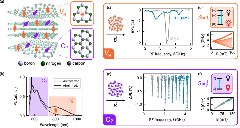
In this Article, we demonstrate the co-existence of two distinct optically addressable spin species in hBN. The two spin defects at the heart of this work are represented in Fig. 1(a). The first is the defect, which emits in the near-infrared [1]. The second spin species is the carbon-related defect emitting in the visible, which we will refer to as – a proposed candidate is the carbon trimer C2CN [28, 29].
We first consider a commercially sourced hBN powder, which was found to naturally contain a high density of defects. Indeed, a photoluminescence (PL) spectrum of the as-received powder under laser excitation ( nm wavelength) shows visible PL emission characteristic of the defect [21], mainly centred around -650 nm with a tail extending in the near-infrared up to 900 nm [Fig. 1(b)]. To create defects, the as-received powder was irradiated with high-energy electrons, causing the appearance of a broad near-infrared emission peak centered around 820 nm characteristic [1] of the defect [Fig. 1(b)].
Next, we used radiofrequency (RF) fields to probe the spin transitions of the defects via spin-dependent PL. A continuous-wave ODMR spectrum of the defect ensemble is obtained by collecting the near-infrared emission (750-1000 nm) as a function of RF frequency [Fig. 1(c)]. Under zero magnetic field (), a single resonance at GHz is observed corresponding to the nearly degenerate electronic spin transitions [see energy level diagram in Fig. 1(d)]. Upon applying a magnetic field, this central resonance splits into two broad resonances due to the Zeeman effect, where the significant broadening is the result of the random orientation of the defects in the powder, as shown in the resonance frequencies calculated for a range of orientations [Fig. 1(d)].
On the other hand, the ODMR spectrum of the defects (550-700 nm) shows a single resonance at a frequency (with natural linewidth 20 MHz) that scales linearly with the applied field [Fig. 1(e)], thus resembling a electronic system. Fitting the data with where is Planck’s constant and the Bohr magneton, yields a -factor of [Fig. 1(f)].
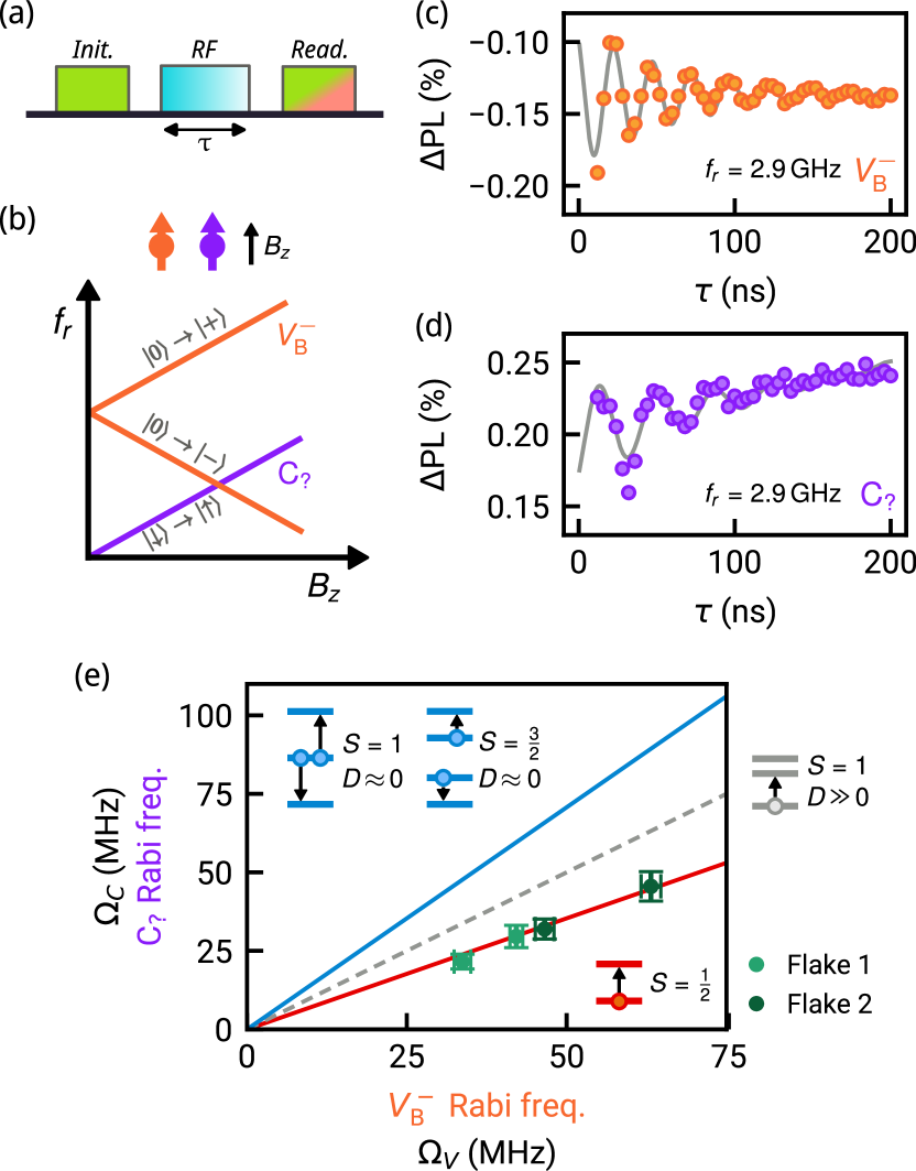
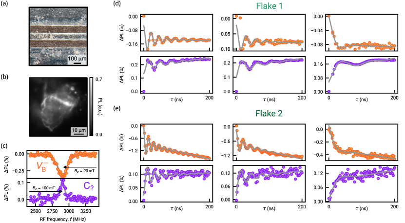
To demonstrate coherent spin control, we perform a Rabi experiment whereby each spin ensemble is driven by a resonant RF pulse of variable duration and the corresponding PL monitored [Fig. 2(a)]. For this purpose, we use a single-crystal hBN flake exfoliated from a bulk hBN sample that has been subjected to a similar electron irradiation as the hBN powder and also naturally contained a high density of defects. The well-defined crystal orientation allows us to align the magnetic field with the spin’s quantization axis (-axis) and drive a single spin transition, e.g. [Fig. 2(b)]. Rabi oscillations are observed both for the ensemble [Fig. 2(c)] and the ensemble [Fig. 2(d)], demonstrating coherent control and optical readout of two distinct spin species within the same host material, at room temperature.
We now address the question of the spin multiplicity of the defect. It has been previously suggested that the visible hBN emitter may be a spin or with a negligible zero-field splitting [23], as this would also be consistent with the observed linear relationship between and , as well as ODMR generally being facilitated by a high spin . Here we provide unambiguous evidence that the visible emitters are in fact true spin doublets, . Namely, we make use of the fact that the Rabi flopping frequency directly depends on the spin multiplicity of the driven species. For a given RF field strength, the ratio between the Rabi frequency of the ensemble () and that of the ensemble () should be if or , and if (see details in the SI, Sec. IV). The results are in good agreement with the latter scenario, and rule out the former [Fig. 2(e)].
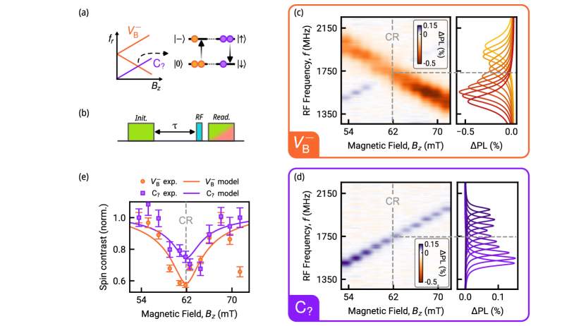
We now study the dynamics and interplay between the two spin species. To this end, we use again a single-crystal hBN sample containing both and spins, and apply a magnetic field to tune the transition of the spins in resonance with the transition of the spins [Fig. 3(a)]. At the resonant field of mT where is the -factor [1], the two spin ensembles can exchange energy causing an increased relaxation of their respective spin populations [Fig. 3(a)], a process known as cross-relaxation (CR) [30, 31].
To probe the CR resonance, we performed pulsed ODMR of both spin species while varying the field strength . In order to allow significant CR to occur, we include an interaction time between the initial laser pulse (which polarises both spin species) and the probe RF pulse [Fig. 3(b)]. Using this sequence, the ensemble experiences a reduced ODMR contrast at the CR resonance [Fig. 3(c)], indicating coupling with a bath of spins including the defects [32, 33]. Crucially, the defects also exhibit a reduced contrast at the CR resonance [Fig. 3(d)], providing unambiguous evidence of - coupling. The normalised ODMR contrast, which is a measure of the amount of spin polarisation following the interaction time , is plot against in Fig. 3(e).
We model the CR effect by considering the coupling of each spin to its nearest neighbour from the opposite spin species (see details in the SI, Sec. VI). For the spins, the mean distance of the nearest is approximately 5 nm based on the estimated density of cm-3 (see SI, Sec. III). The resulting model with no free parameter [purple line in Fig. 3(e)] is in good agreement with the data, confirming that we do indeed detect CR between the and spin ensembles. For the case, we leave the total density of spins free; best fit to the data is achieved for cm-3. The demonstrated coupling between two optically addressable spin species of different multiplicities will be an important resource for quantum simulation applications.
Having established the nature of the defect, we now explore its potential for quantum sensing and imaging. The key advantage of the spin is its lack of intrinsic quantization axis, which means magnetometry can be performed under any direction of the external magnetic field. This feature is in contrast to spin defects with uniaxial anisotropy such as the defect or the nitrogen-vacancy centre in diamond which are restricted to a narrow range of field directions and magnitudes due to spin mixing caused by transverse fields [34]. Moreover, the isotropic response of the spin defect means powdered hBN samples with random crystal orientation can be employed, offering a convenient, cost-effective alternative to single-crystal exfoliated flakes.
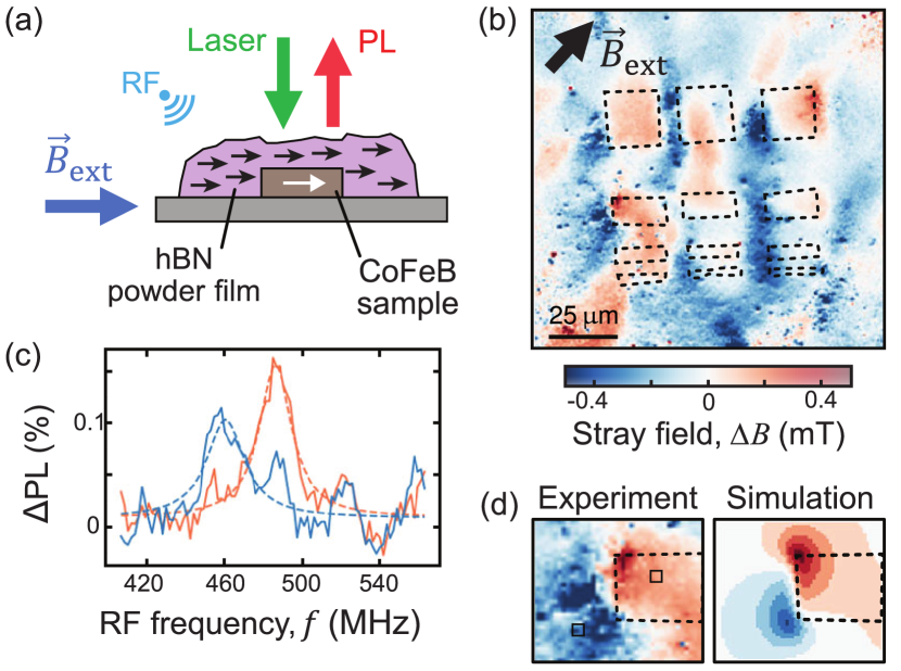
To demonstrate these two features enabled by the defect, we prepared a film of hBN powder on a test magnetic sample (a patterned CoFeB film with in-plane magnetization) and used the hBN film to spatially map the sample’s stray magnetic field [Fig. 4(a)] at room temperature. Magnetic field mapping is achieved by performing widefield ODMR measurements of the defects under an in-plane bias magnetic field (strength mT). At each pixel of the image, the measured resonance frequency is converted to a total magnetic field where is the sample’s stray field projected along the direction of the external field (assuming ). The obtained map [Fig. 4(b)] correlates with the magnetic structures, as shown by the dashed rectangles. The stray field varies by up to mT across the image corresponding to Zeeman shifts of MHz, see example ODMR spectra in Fig. 4(c). The measured field is also in good agreement with simulations both quantitatively and in terms of the overall pattern, as shown in Fig. 4(d).
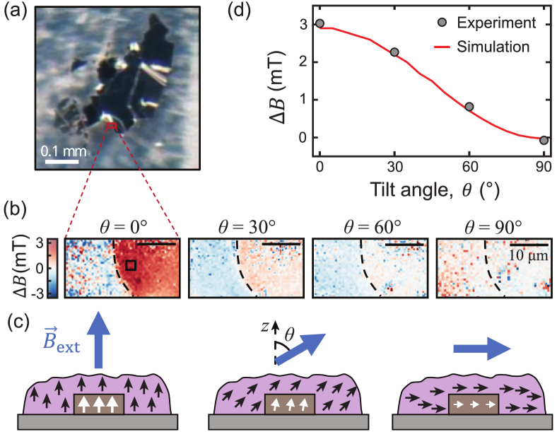
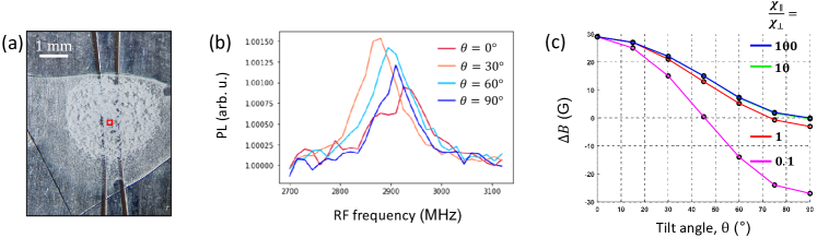
As a final experiment, we performed magnetic imaging at cryogenic temperature ( K) while varying the direction of the external magnetic field. Here the test magnetic sample is a crystal of Fe3GeTe2 [Fig. 5(a)], a ferromagnetic van der Waals material with a Curie temperature of K [35, 36]. Following zero-field cooling, we applied a field of strength mT and performed magnetic field imaging via ODMR of the defects as explained above, for various angles between and the -axis of the Fe3GeTe2 crystal ( axis). The resulting stray field maps taken near an edge of the crystal [Fig. 5(b)] show a gradual decrease in as is increased from (i.e. parallel to the -axis) to ( perpendicular to the -axis). This decrease can be explained by the strong perpendicular magnetic anisotropy of Fe3GeTe2, which in the bulk regime is a soft ferromagnet with a magnetic susceptibility ratio ranging from about 2 to 10 depending on the exact Fe content [35, 36], where () is the susceptibility parallel (perpendicular) to the -axis. To estimate the ratio in our sample, we simulate the stray field at the different angles , taking into account both the rotation of the projection axis of and the effect on the sample’s magnetization, namely a reduction in magnitude and a canting of the magnetization vector as is increased, as illustrated in Fig. 5(c). We find that the simulation matches well the data for [Fig. 5(d)].
Compared with mature solid-state spin sensors such as the nitrogen-vacancy centre in diamond, our sensor is decoupled from the symmetries of the host crystal structure while retaining the convenience of robust optical operation and natural compatibility with quantitative imaging. These features allow for operation with arbitrarily oriented bias fields, that may be aligned (or misaligned) with respect to the symmetry axis of the sample in order to uncover a greater range of magnetic behaviours. Moreover, the hBN film also concurrently hosts defects which can be used for temperature mapping through monitoring of the zero-field splitting [13, 14, 15]. This multi-modal capability is unique to the hBN powder platform where the individual particles are not in thermal contact with each other allowing for minimally invasive temperature sensing, concurrent with arbitrary-direction magnetometry, making it ideally suited for studies of phase transitions.
More generally, the co-existence of two distinct spin ensembles within a single host material, which can both be optically initialised, read out, and coherently driven, at room temperature, distinguishes hBN from established material platforms such as diamond and silicon carbide in which only one type of optically addressable spin defect can generally be stabilised in a given sample [37]. The nature of one of these spin ensembles is also unique to hBN. These attributes already open new modalities for quantum sensing and imaging as discussed above, as well as unique opportunities for many-body quantum dynamics and quantum simulations. Furthermore, reaching the regime of 2D confinement, i.e. where the vertical extent of the spin ensemble is less than the typical distance between neighbouring spins, is a realistic prospect given the recent observation of defects in few-layer hBN [5]. Such a 2D confinement would pave the way towards 2D spin-based quantum simulators, which could exploit not only the disordered ensembles of directly controllable electron spins studied here, but also the ordered lattice of strongly interacting nuclear spins intrinsic to hBN [38, 20]. Isotope engineering [32] offers further room for tuning the parameters of this rich electron-nuclear spin system. The hBN platform thus emerges as a promising system for realising a scalable quantum simulator to simulate a wide variety of strongly correlated spin models [39].
Acknowledgements.
This work was supported by the Australian Research Council (ARC) through grants CE170100012, CE200100010, FT200100073, FT220100053, DE200100279, DE230100192, and DP220100178, and by the Office of Naval Research Global (N62909-22-1-2028). The work was performed in part at the RMIT Micro Nano Research Facility (MNRF) in the Victorian Node of the Australian National Fabrication Facility (ANFF). The authors acknowledge the facilities, and the scientific and technical assistance of the RMIT Microscopy & Microanalysis Facility (RMMF), a linked laboratory of Microscopy Australia, enabled by NCRIS. S.C.S gratefully acknowledges the support of an Ernst and Grace Matthaei scholarship. I.O.R. is supported by an Australian Government Research Training Program Scholarship. G.H. is supported by the University of Melbourne through a Melbourne Research Scholarship. P.R. acknowledges support through an RMIT University Vice-Chancellor’s Research Fellowship. Part of this study was supported by QST President’s Strategic Grant “QST International Research Initiative”.References
- Gottscholl et al. [2020] A. Gottscholl, M. Kianinia, V. Soltamov, S. Orlinskii, G. Mamin, C. Bradac, C. Kasper, K. Krambrock, A. Sperlich, M. Toth, I. Aharonovich, and V. Dyakonov, Initialization and read-out of intrinsic spin defects in a van der waals crystal at room temperature, Nature Materials 19, 540 (2020).
- Liu et al. [2022a] W. Liu, N.-J. Guo, S. Yu, Y. Meng, Z.-P. Li, Y.-Z. Yang, Z.-A. Wang, X.-D. Zeng, L.-K. Xie, Q. Li, J.-F. Wang, J.-S. Xu, Y.-T. Wang, J.-S. Tang, C.-F. Li, and G.-C. Guo, Spin-active defects in hexagonal boron nitride, Materials for Quantum Technology 2, 032002 (2022a).
- Aharonovich et al. [2022] I. Aharonovich, J.-P. Tetienne, and M. Toth, Quantum emitters in hexagonal boron nitride, Nano Letters 22, 9227 (2022).
- Vaidya et al. [2023] S. Vaidya, X. Gao, S. Dikshit, I. Aharonovich, and T. Li, Quantum sensing and imaging with spin defects in hexagonal boron nitride, Advances in Physics: X 8, 2206049 (2023).
- Durand et al. [2023] A. Durand, T. Clua-Provost, F. Fabre, P. Kumar, J. Li, J. H. Edgar, P. Udvarhelyi, A. Gali, X. Marie, C. Robert, J. M. Gérard, B. Gil, G. Cassabois, and V. Jacques, Optically-active spin defects in few-layer thick hexagonal boron nitride, Preprint , arXiv:2304.12071 (2023).
- Yao et al. [2018] N. Y. Yao, M. P. Zaletel, D. M. Stamper-Kurn, and A. Vishwanath, A quantum dipolar spin liquid, Nature Physics 14, 405 (2018).
- Davis et al. [2023] E. J. Davis, B. Ye, F. Machado, S. A. Meynell, W. Wu, T. Mittiga, W. Schenken, M. Joos, B. Kobrin, Y. Lyu, Z. Wang, D. Bluvstein, S. Choi, C. Zu, A. C. B. Jayich, and N. Y. Yao, Probing many-body dynamics in a two-dimensional dipolar spin ensemble, Nature Physics 19, 836 (2023).
- Choi et al. [2016] J.-y. Choi, S. Hild, J. Zeiher, P. Schauß, A. Rubio-Abadal, T. Yefsah, V. Khemani, D. A. Huse, I. Bloch, and C. Gross, Exploring the many-body localization transition in two dimensions, Science (New York, N.Y.) 352, 1547 (2016).
- Choi et al. [2017] S. Choi, J. Choi, R. Landig, G. Kucsko, H. Zhou, J. Isoya, F. Jelezko, S. Onoda, H. Sumiya, V. Khemani, et al., Observation of discrete time-crystalline order in a disordered dipolar many-body system, Nature 543, 221 (2017).
- Abanin et al. [2019] D. A. Abanin, E. Altman, I. Bloch, and M. Serbyn, Colloquium: Many-body localization, thermalization, and entanglement, Reviews of Modern Physics 91, 021001 (2019).
- Zu et al. [2021] C. Zu, F. Machado, B. Ye, S. Choi, B. Kobrin, T. Mittiga, S. Hsieh, P. Bhattacharyya, M. Markham, D. Twitchen, et al., Emergent hydrodynamics in a strongly interacting dipolar spin ensemble, Nature 597, 45 (2021).
- Gong et al. [2023] R. Gong, G. He, X. Gao, P. Ju, Z. Liu, B. Ye, E. A. Henriksen, T. Li, and C. Zu, Coherent dynamics of strongly interacting electronic spin defects in hexagonal boron nitride, Nature Communications 14, 3299 (2023).
- Gottscholl et al. [2021] A. Gottscholl, M. Diez, V. Soltamov, C. Kasper, D. Krausse, A. Sperlich, M. Kianinia, C. Bradac, I. Aharonovich, and V. Dyakonov, Spin defects in hBN as promising temperature, pressure and magnetic field quantum sensors, Nature Communications 12, 4480 (2021).
- Liu et al. [2021] W. Liu, Z.-P. Li, Y.-Z. Yang, S. Yu, Y. Meng, Z.-A. Wang, Z.-C. Li, N.-J. Guo, F.-F. Yan, Q. Li, J.-F. Wang, J.-S. Xu, Y.-T. Wang, J.-S. Tang, C.-F. Li, and G.-C. Guo, Temperature-dependent energy-level shifts of spin defects in hexagonal boron nitride, ACS Photonics 8, 1889 (2021).
- Healey et al. [2023] A. J. Healey, S. C. Scholten, T. Yang, J. A. Scott, G. J. Abrahams, I. O. Robertson, X. F. Hou, Y. F. Guo, S. Rahman, Y. Lu, M. Kianinia, I. Aharonovich, and J.-P. Tetienne, Quantum microscopy with van der waals heterostructures, Nature Physics 19, 87 (2023).
- Huang et al. [2022] M. Huang, J. Zhou, D. Chen, H. Lu, N. J. McLaughlin, S. Li, M. Alghamdi, D. Djugba, J. Shi, H. Wang, and C. R. Du, Wide field imaging of van der waals ferromagnet Fe3GeTe2 by spin defects in hexagonal boron nitride, Nature Communications 13, 5369 (2022).
- Lyu et al. [2022] X. Lyu, Q. Tan, L. Wu, C. Zhang, Z. Zhang, Z. Mu, J. Zúñiga-Pérez, H. Cai, and W. Gao, Strain quantum sensing with spin defects in hexagonal boron nitride, Nano Letters 22, 6553 (2022).
- Kumar et al. [2022] P. Kumar, F. Fabre, A. Durand, T. Clua-Provost, J. Li, J. Edgar, N. Rougemaille, J. Coraux, X. Marie, P. Renucci, C. Robert, I. Robert-Philip, B. Gil, G. Cassabois, A. Finco, and V. Jacques, Magnetic imaging with spin defects in hexagonal boron nitride, Physical Review Applied 18, L061002 (2022).
- Robertson et al. [2023] I. O. Robertson, S. C. Scholten, P. Singh, A. J. Healey, F. Meneses, P. Reineck, H. Abe, T. Ohshima, M. Kianinia, I. Aharonovich, and J.-P. Tetienne, Detection of paramagnetic spins with an ultrathin van der waals quantum sensor, Preprint , arXiv:2302.10560 (2023).
- Gao et al. [2023] X. Gao, S. Vaidya, P. Ju, S. Dikshit, K. Shen, Y. P. Chen, and T. Li, Quantum sensing of paramagnetic spins in liquids with spin qubits in hexagonal boron nitride, Preprint , arXiv:2303.02326 (2023).
- Mendelson et al. [2021] N. Mendelson, D. Chugh, J. R. Reimers, T. S. Cheng, A. Gottscholl, H. Long, C. J. Mellor, A. Zettl, V. Dyakonov, P. H. Beton, S. V. Novikov, C. Jagadish, H. H. Tan, M. J. Ford, M. Toth, C. Bradac, and I. Aharonovich, Identifying carbon as the source of visible single-photon emission from hexagonal boron nitride, Nature Materials 20, 321 (2021).
- Chejanovsky et al. [2021] N. Chejanovsky, A. Mukherjee, J. Geng, Y.-C. Chen, Y. Kim, A. Denisenko, A. Finkler, T. Taniguchi, K. Watanabe, D. B. R. Dasari, et al., Single-spin resonance in a van der waals embedded paramagnetic defect, Nature Materials 20, 1079 (2021).
- Stern et al. [2022] H. L. Stern, Q. Gu, J. Jarman, S. Eizagirre Barker, N. Mendelson, D. Chugh, S. Schott, H. H. Tan, H. Sirringhaus, I. Aharonovich, and M. Atature, Room-temperature optically detected magnetic resonance of single defects in hexagonal boron nitride, Nature Communications 13, 618 (2022).
- Guo et al. [2023] N.-J. Guo, S. Li, W. Liu, Y.-Z. Yang, X.-D. Zeng, S. Yu, Y. Meng, Z.-P. Li, Z.-A. Wang, L.-K. Xie, R.-C. Ge, J.-F. Wang, Q. Li, J.-S. Xu, Y.-T. Wang, J.-S. Tang, A. Gali, C.-F. Li, and G.-C. Guo, Coherent control of an ultrabright single spin in hexagonal boron nitride at room temperature, Nature Communications 14, 2893 (2023).
- Yang et al. [2023] Y.-Z. Yang, T.-X. Zhu, Z.-P. Li, X.-D. Zeng, N.-J. Guo, S. Yu, Y. Meng, Z.-A. Wang, L.-K. Xie, Z.-Q. Zhou, Q. Li, J.-S. Xu, X.-Y. Gao, W. Liu, Y.-T. Wang, J.-S. Tang, C.-F. Li, and G.-C. Guo, Laser direct writing of visible spin defects in hexagonal boron nitride for applications in spin-based technologies, ACS Applied Nano Materials 6, 6407 (2023).
- Auburger and Gali [2021] P. Auburger and A. Gali, Towards ab initio identification of paramagnetic substitutional carbon defects in hexagonal boron nitride acting as quantum bits, Physical Review B 104, 075410 (2021).
- Jara et al. [2021] C. Jara, T. Rauch, S. Botti, M. A. L. Marques, A. Norambuena, R. Coto, J. E. Castellanos-Águila, J. R. Maze, and F. Munoz, First-principles identification of single photon emitters based on carbon clusters in hexagonal boron nitride, The Journal of Physical Chemistry A 125, 1325 (2021).
- Golami et al. [2022] O. Golami, K. Sharman, R. Ghobadi, S. C. Wein, H. Zadeh-Haghighi, C. Gomes da Rocha, D. R. Salahub, and C. Simon, Ab initio and group theoretical study of properties of a carbon trimer defect in hexagonal boron nitride, Physical Review B 105, 184101 (2022).
- Li et al. [2022] K. Li, T. J. Smart, and Y. Ping, Carbon trimer as a 2 eV single-photon emitter candidate in hexagonal boron nitride: A first-principles study, Physical Review Materials 6, L042201 (2022).
- Hall et al. [2016] LT. Hall, P. Kehayias, DA. Simpson, A. Jarmola, A. Stacey, D. Budker, and LCL. Hollenberg, Detection of nanoscale electron spin resonance spectra demonstrated using nitrogen-vacancy centre probes in diamond, Nature Communications 7, 10211 (2016).
- Broadway et al. [2018] D. A. Broadway, J.-P. Tetienne, A. Stacey, J. D. Wood, D. A. Simpson, L. T. Hall, and L. C. Hollenberg, Quantum probe hyperpolarisation of molecular nuclear spins, Nature Communications 9, 1246 (2018).
- Haykal et al. [2022] A. Haykal, R. Tanos, N. Minotto, A. Durand, F. Fabre, J. Li, J. H. Edgar, V. Ivády, A. Gali, T. Michel, A. Dréau, B. Gil, G. Cassabois, and V. Jacques, Decoherence of VB- spin defects in monoisotopic hexagonal boron nitride, Nature Communications 13, 1 (2022).
- Baber et al. [2022] S. Baber, R. N. E. Malein, P. Khatri, P. S. Keatley, S. Guo, F. Withers, A. J. Ramsay, and I. J. Luxmoore, Excited state spectroscopy of boron vacancy defects in hexagonal boron nitride using time-resolved optically detected magnetic resonance, Nano Letters 22, 461 (2022).
- Tetienne et al. [2012] J.-P. Tetienne, L. Rondin, P. Spinicelli, M. Chipaux, T. Debuisschert, J.-F. Roch, and V. Jacques, Magnetic-field-dependent photodynamics of single NV defects in diamond: An application to qualitative all-optical magnetic imaging, New Journal of Physics 14, 103033 (2012).
- Chen et al. [2013] B. Chen, J. Yang, H. Wang, M. Imai, H. Ohta, C. Michioka, K. Yoshimura, and M. Fang, Magnetic properties of layered itinerant electron ferromagnet Fe3GeTe2, Journal of the Physical Society of Japan 82, 124711 (2013).
- May et al. [2016] A. F. May, S. Calder, C. Cantoni, H. Cao, and M. A. McGuire, Magnetic structure and phase stability of the van der waals bonded ferromagnet Fe3-xGeTe2, Physical Review B 93, 014411 (2016).
- Wolfowicz et al. [2021] G. Wolfowicz, F. J. Heremans, C. P. Anderson, S. Kanai, H. Seo, A. Gali, G. Galli, and D. D. Awschalom, Quantum guidelines for solid-state spin defects, Nature Reviews Materials 6, 906 (2021).
- Murzakhanov et al. [2022] F. F. Murzakhanov, G. V. Mamin, S. B. Orlinskii, U. Gerstmann, W. G. Schmidt, T. Biktagirov, I. Aharonovich, A. Gottscholl, A. Sperlich, V. Dyakonov, and V. A. Soltamov, Electron-nuclear coherent coupling and nuclear spin readout through optically polarized VB spin states in hBN, Nano Letters 22, 2718 (2022).
- Cai et al. [2013] J. Cai, A. Retzker, F. Jelezko, and M. B. Plenio, A large-scale quantum simulator on a diamond surface at room temperature, Nature Physics 9, 168 (2013).
- Lillie et al. [2020] S. E. Lillie, D. A. Broadway, N. Dontschuk, S. C. Scholten, B. C. Johnson, S. Wolf, S. Rachel, L. C. L. Hollenberg, and J.-P. Tetienne, Laser modulation of superconductivity in a cryogenic wide-field nitrogen-vacancy microscope, Nano Letters 20, 1855 (2020).
- Broadway et al. [2020] D. A. Broadway, S. C. Scholten, C. Tan, N. Dontschuk, S. E. Lillie, B. C. Johnson, G. Zheng, Z. Wang, A. R. Oganov, S. Tian, C. Li, H. Lei, L. Wang, L. C. L. Hollenberg, and J.-P. Tetienne, Imaging domain reversal in an ultrathin van der waals ferromagnet, Advanced Materials 32, 2003314 (2020).
- Chen et al. [2021] Y. Chen, C. Li, S. White, M. Nonahal, Z.-Q. Xu, K. Watanabe, T. Taniguchi, M. Toth, T. T. Tran, and I. Aharonovich, Generation of high-density quantum emitters in high-quality, exfoliated hexagonal boron nitride, ACS Applied Materials & Interfaces 13, 47283 (2021).
- Liu et al. [2022b] H. Liu, N. Mendelson, I. H. Abidi, S. Li, Z. Liu, Y. Cai, K. Zhang, J. You, M. Tamtaji, H. Wong, Y. Ding, G. Chen, I. Aharonovich, and Z. Luo, Rational control on quantum emitter formation in carbon-doped monolayer hexagonal boron nitride, ACS Applied Materials & Interfaces 14, 3189 (2022b).
- Neumann et al. [2023] M. Neumann, X. Wei, L. Morales-Inostroza, S. Song, S.-G. Lee, K. Watanabe, T. Taniguchi, S. Götzinger, and Y. H. Lee, Organic molecules as origin of visible-range single photon emission from hexagonal boron nitride and mica, ACS Nano 10.1021/acsnano.3c02348 (2023).
- Mathur et al. [2022] N. Mathur, A. Mukherjee, X. Gao, J. Luo, B. A. McCullian, T. Li, A. N. Vamivakas, and G. D. Fuchs, Excited-state spin-resonance spectroscopy of VB- defect centers in hexagonal boron nitride, Nature Communications 13, 3233 (2022).
- Mu et al. [2022] Z. Mu, H. Cai, D. Chen, J. Kenny, Z. Jiang, S. Ru, X. Lyu, T. S. Koh, X. Liu, I. Aharonovich, and W. Gao, Excited-state optically detected magnetic resonance of spin defects in hexagonal boron nitride, Physical Review Letters 128, 216402 (2022).
- Yu et al. [2022] P. Yu, H. Sun, M. Wang, T. Zhang, X. Ye, J. Zhou, H. Liu, C.-J. Wang, F. Shi, Y. Wang, and J. Du, Excited-state spectroscopy of spin defects in hexagonal boron nitride, Nano Letters 22, 3545 (2022).
- Murzakhanov et al. [2021] F. F. Murzakhanov, B. V. Yavkin, G. V. Mamin, S. B. Orlinskii, I. E. Mumdzhi, I. N. Gracheva, B. F. Gabbasov, A. N. Smirnov, V. Y. Davydov, and V. A. Soltamov, Creation of negatively charged boron vacancies in hexagonal boron nitride crystal by electron irradiation and mechanism of inhomogeneous broadening of boron vacancy-related spin resonance lines, Nanomaterials (Basel, Switzerland) 11, 1373 (2021).
- Bonamente [2017] M. Bonamente, Goodness of fit and parameter uncertainty, in Statistics and Analysis of Scientific Data, Graduate Texts in Physics, edited by M. Bonamente (Springer, New York, NY, 2017) pp. 177–193.
- Hall et al. [2014] L. T. Hall, J. H. Cole, and L. C. L. Hollenberg, Analytic solutions to the central-spin problem for nitrogen-vacancy centers in diamond, Physical Review B 90, 075201 (2014).
- Wood et al. [2016] J. D. A. Wood, D. A. Broadway, L. T. Hall, A. Stacey, D. A. Simpson, J.-P. Tetienne, and L. C. L. Hollenberg, Wide-band nanoscale magnetic resonance spectroscopy using quantum relaxation of a single spin in diamond, Physical Review B 94, 155402 (2016).
- Scholten et al. [2021] S. C. Scholten, A. J. Healey, I. O. Robertson, G. J. Abrahams, D. A. Broadway, and J.-P. Tetienne, Widefield quantum microscopy with nitrogen-vacancy centers in diamond: Strengths, limitations, and prospects, Journal of Applied Physics 130, 150902 (2021).
- Rondin et al. [2012] L. Rondin, J.-P. Tetienne, P. Spinicelli, C. Dal Savio, K. Karrai, G. Dantelle, A. Thiaville, S. Rohart, J.-F. Roch, and V. Jacques, Nanoscale magnetic field mapping with a single spin scanning probe magnetometer, Applied Physics Letters 100, 10.1063/1.3703128 (2012).
- Tan et al. [2018] C. Tan, J. Lee, S.-g. Jung, T. Park, S. Albarakati, J. Partridge, M. R. Field, D. G. McCulloch, L. Wang, and C. Lee, Hard magnetic properties in nanoflake van der waals Fe3GeTe2, Nature Communications 9, 1554 (2018).
Supplementary Information for the manuscript “Multi-species optically addressable spin defects in a van der Waals material at room temperature”
I Experimental setup
The optical and spin measurements reported in Fig. 1-3 of the main text [except Fig. 1(e)] were carried out on a custom-built wide-field fluorescence microscope. Optical excitation from a continuous-wave (CW) nm laser (Laser Quantum Opus 2 W) was gated using an acousto-optic modulator (Gooch & Housego R35085-5) and focused using a widefield lens ( mm) to the back aperture of the objective lens (Nikon S Plan Fluor ELWD 20x, NA = 0.45). The photoluminescence (PL) from the samples is separated from the excitation light with a dichroic mirror and a 550 nm longpass filter. The PL is either sent to a spectrometer (Ocean Insight Maya2000-Pro) or imaged with a scientific CMOS camera (Andor Zyla 5.5-W USB3) using a mm tube lens. When imaging, additional shortpass and longpass optical filters were inserted to only collect a given wavelength range. The laser spot diameter () at the sample was about 50 m and the total CW laser power 500 mW, which gives a maximum intensity of about 0.5 mWm2 in the centre of the spot. Radiofrequency (RF) driving was provided by a signal generator (Windfreak SynthNV PRO) gated using an IQ modulator (Texas Instruments TRF37T05EVM) and amplified (Mini-Circuits HPA-50W-63+). A pulse pattern generator (SpinCore PulseBlasterESR-PRO 500 MHz) was used to gate the excitation laser and RF, as well as for triggering the camera. The output of the amplifier was connected to a printed circuit board (PCB) equipped with a coplanar waveguide and terminated by a 50 termination. The external magnetic field was applied using a permanent magnet. The field was approximately oriented along the -axis of the lab frame (i.e. perpendicular to the plane of the hBN films or flakes) and for each position of the magnet the field strength was estimated using ODMR of defects in a reference bulk hBN crystal as well as of nitrogen-vacancy centres in a reference diamond. All measurements were performed at room temperature in ambient atmosphere.
For Fig. 4 of the main text, a nearly identical setup to that described above was used with the following differences. First, the RF field was delivered using a loop antenna terminating a coaxial cable, rather than using a PCB. Second, the laser spot diameter at the sample was enlarged to about 100 m in order to access a larger field of view, and the CW laser power was reduced to 200 mW. Finally, the bias magnetic field was oriented in the plane of the sample, applied using a permanent magnet.
For Fig. 5 of the main text, the overall setup was similar to that described above except that parts of the setup (sample, PCB, objective lens) were enclosed in a closed-cycle cryostat, as described in Refs. [40, 41]. The measurements were taken at the base temperature ( K) in a helium exchange gas. The magnetic field was applied using a superconducting vector magnet, allowing us to precisely control both the direction and magnitude of the applied magnetic field. This setup was also used to obtain the field-dependent ODMR spectra in Fig. 1(e) of the main text.
II Preparation and additional characterisation of hBN powder samples
II.1 Sample preparation
The experiments reported in Figs. 1, 4 and 5 of the main text used hBN nanopowder sourced from Graphene Supermarket (BN Ultrafine Powder), which has a specified purity of 99.0%. Two batches of powder nominally identical but purchased at different times were used: ‘Powder 1’ was purchased in 2022 whereas ‘Powder 2’ was purchased in 2017. The as-received powders were electron irradiated with a beam energy of 2 MeV and a variable dose between cm-2 and cm-2. No annealing or further processing was performed. The experiments reported in Fig. 1 used Powder 1 with a dose of cm-2, whereas the experiments reported in Fig. 4 and Fig. 5 used Powder 2 with a dose of cm-2.
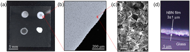
To form thin films of the hBN powders, the powder was suspended in isopropyl alcohol (IPA) at a concentration of 20 mg/mL and sonicated for 30 min using a horn-sonicator. The sediment from the suspension was drawn using a pipette then drop-cast on a glass coverslip, generally forming a relatively continuous film as shown in Fig. S1(a,b). Although individual flakes have a thickness of nm and a lateral size of nm [19], a scanning electron microscopy image [Fig. S1(c)] reveals aggregates with a size of m. To estimate the thickness of the films, we cleaved the coverslip across the film and inspected the cross-section using an optical microscope [Fig. S1(d)], indicating a typical film thickness of a few micrometers.
II.2 Optical characterisation
Here we present additional optical and spin characterisation of the hBN powders used in this work, including a comparison of the two batches of powder (Powder 1 and Powder 2) and of the different irradiation doses. The PL spectra of the different powders under green laser excitation (wavelength nm) are plotted in Fig. S2(a).
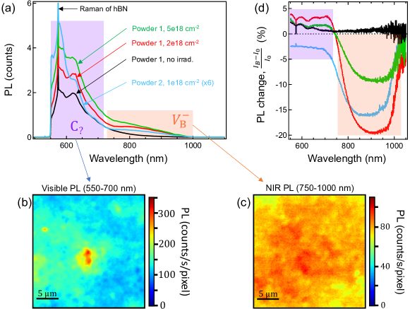
Considering first Powder 1 samples that received different doses of electron irradiation, we observe the appearance of a broad near-infrared (NIR) emission peak centered around 820 nm, with an amplitude correlating with the irradiation dose, indicating the successful creation of defects. In addition to the characteristic emission, all samples emit PL in the visible region ( nm) including in the non-irradiated (as-received) powder, with a tail extending in the NIR (up to 900 nm). Similar PL emission was previously observed in various hBN samples [21, 42, 43, 25] and was attributed to carbon-related defects, often referred to in the literature as the 2 eV emitters. It was also suggested that polycyclic aromatic hydrocarbon (PAH) molecules trapped within the hBN crystal or at interfaces may be responsible for this 2 eV emission [44], rather than proper crystalline point defect. In the main text, we call the visible emitters present in our samples defects to remind that they are carbon-related but that their exact structure remains unknown.
Interestingly, it can be seen in Fig. S2(a) that electron irradiation increases the amplitude of the visible PL signal, by approximately two fold for the highest dose ( cm-2) compared to the non-irradiated case. Compared to the Powder 1 samples, Powder 2 (irradiated to cm-2) emits significantly less visible PL (there is a multiplying factor of in Fig. S2(a) for Powder 2) and has a slightly different spectral distribution, indicating that the concentration and specific optical properties of the defects is variable from batch to batch. To assess the spatial homogeneity of the films, we recorded widefield PL images of an irradiated Powder 1 sample [Fig. S2(b,c)]. While the emission is relatively uniform [Fig. S2(c)], the visible emission appears more patchy [Fig. S2(b)], indicating that the density of defects varies within a given sample. Nevertheless, the visible emission is continuous for the micrometer-thick films studied here, i.e. there is no dark region with no visible PL. This feature is important to allow for magnetic imaging using the defects as demonstrated in Fig. 4 of the main text.
As a first test to probe whether the defects responsible for the observed PL emission are spin-active, we applied an external magnetic field ( mT) and observed its effect on the PL spectrum [Fig. S2(d)]. In the NIR region (750-1000 nm), the PL drops by 5-20% in all samples except the non-irradiated powder which experiences less than 1% change. This field-induced PL quenching is due to spin mixing of the defects [33, 45, 46, 47], which in a powder have a randomly oriented quantization axis with respect to the field direction. In the visible region (550-700 nm), all samples respond to the applied magnetic field to varying degrees. Surprisingly, the Powder 1 samples exhibit a PL increase (by 1-4%) while the Powder 2 sample sees a decreased PL (by 2-3%). The field-induced PL change extends over the entire 550-700 nm range.
II.3 Spin characterisation
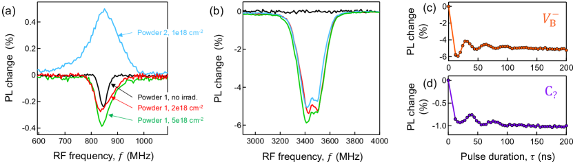
ODMR spectra of the same set of powder samples are shown in Fig. S3(a,b) for the and defects, respectively. For the case where only the visible PL (550-700 nm) is collected [Fig. S3(a)], the ODMR spectra show a single resonance at frequency in all cases (), but for Powder 1 samples the contrast is negative whereas it is positive for the Powder 2 sample. The sign of the ODMR contrast anti-correlates with the sign of the PL change due to applying a magnetic field [Fig. S2(d)]. That is, where applying a static magnetic field increases (decreases) the PL, then driving the spin transition under this applied static field decreases (increases) the PL. This observation points to a mechanism whereby the spin dependence of the optical transitions is enhanced by the static field rather than reduced due to spin mixing, as is the case for the defect or the nitrogen-vacancy centre in diamond [34]. We also observed opposite signs from different spatial locations within the same powder sample [Fig. S4], indicating that the variability is inherent to the material itself. The variability in sign of the ODMR contrast within and between samples is currently not understood.
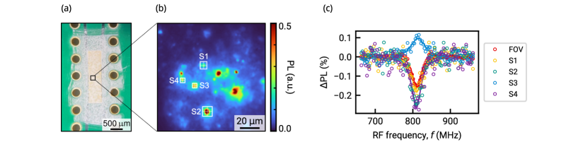
Figure S3(a) further reveals that the ODMR contrast of the defects increases slightly with increased irradiation dose (Powder 1 samples), from about 0.2% for the non-irradiated powder to 0.4% for the highest irradiation dose. Meanwhile, the linewidth (FWHM) of the resonance is also increased, from about 30 MHz to 60 MHz. Powder 2 has a positive contrast of about 0.5% and a significantly larger linewidth of about 200 MHz (in CW ODMR), under identical laser and RF driving conditions. Pulsed ODMR measurements generally led to a significant line narrowing down to about 20 MHz, relatively consistent across all powder samples.
The ODMR spectra at [Fig. S3(b)] show very little difference between the various powder samples, with a contrast of , except for the non-irradiated sample which exhibits no contrast, confirming the absence of defects in this case.
We were able to observe Rabi oscillations in all samples for both spin species where present. Example Rabi oscillations from Powder 1 are shown in Fig. S3(c,d) for and , respectively.
III Preparation and additional characterisation of hBN single-crystal samples
III.1 Sample preparation
The experiments reported in Fig. 2 and 3 of the main text used single-crystal samples, either a whole bulk crystal (in Fig. 3) or a thinner flake exfoliated from a bulk crystal (in Fig. 2). In both cases, the starting whole hBN crystals were sourced from HQ Graphene, and had a thickness of m and a lateral size of mm. The as-received crystals were electron irradiated with a beam energy of 2 MeV and a dose between cm-2 and cm-2. No annealing or further processing was performed.
III.2 Bulk crystal characterisation
A photograph of a typical bulk crystal studied is shown in Fig. S5(a). Domain boundaries are visible, which are believed to be wrinkles that formed during the crystal growth process.
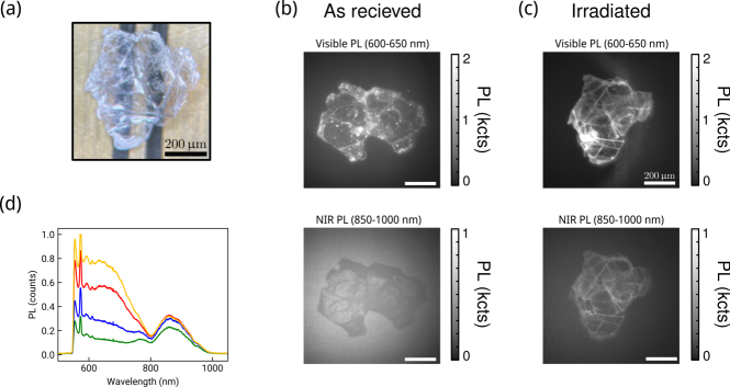
PL images of an as-received crystal [Fig. S5(b)] show no signature of emission but there is some signal in the visible from isolated spots (possibly single emitters) as well as from extended features.
After irradiation, however, the visible PL is overall more intense and homogeneous [top image in Fig. S5(c)], suggesting that the electron irradiation plays a role in activating the defects. There is also enhanced emission from the wrinkles, which appear up to brighter than the regions in between. This could be due to optical effects or indicate a higher density of active optical emitters in the wrinkles. Nevertheless, we were able to detect ODMR from the defects in all regions of the crystal independent of brightness. In addition, the electron irradiation results in NIR PL from defects [bottom image in Fig. S5(c)]. There is a correlation with the wrinkles again, but this is mainly due to the NIR tail of the emission, whereas the PL from the defects is relatively uniform throughout the crystal. This is confirmed by examining PL spectra from various localised regions in the crystal including the bright wrinkles as well as darker regions, a few examples are shown in Fig. S5(d).
For the experiments presented in Fig. 3 of the main text, we used a crystal irradiated with the highest dose of cm-2, in order to create a dense ensemble of defects. In Ref. [48], Murzakhanov et al. characterised a bulk hBN crystal from the same supplier after electron irradiation with a dose of cm-2 at 2 MeV. Through careful analysis of EPR data, they determined a concentration of spins in their sample of cm-3. Given our sample is nominally identical with only a slightly higher irradiation dose (by a factor of 1.67), we can assume that to a good approximation the density in our sample is increased by the same factor, which gives a density of cm-3. This value was used for the analysis of the cross-relaxation experiment, see Sec. VI. For the measurements presented in Fig. 3 of the main text, we used a region of the crystal close to a wrinkle in order to get bright visible emission, which is assumed to correlate with a high density of defect. The latter density is a priori unknown.
III.3 Exfoliated flake characterisation
For the experiments presented in Fig. 2 of the main text, we used a thin flake exfoliated from a bulk crystal similar to that shown in Fig. S5(a,c). Flakes were exfoliated using adhesive tape and transferred directly onto a coplanar waveguide. This process allows for a strong and uniform RF driving field across the flake, required to observe multiple Rabi oscillations and thus analyse the Rabi frequency, see Sec. IV.
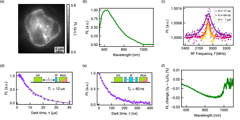
Here we present some characterisation measurements of a typical flake, exfoliated from a crystal irradiated at a dose of cm-2. The PL image (550-700 nm) [Fig. S6(a)] shows relatively uniform visible emission throughout the flake, with some brighter spots and edges but no pronounced wrinkle feature as was seen in Fig. S5(c). The PL spectrum averaged over the entire flake [Fig. S6(b)] is dominated by the visible emission with only a subtle shoulder in the NIR due to the defects, indicating a relatively large density of defects in this flake.
Pulsed ODMR spectra of the defects at mT [Fig. S6(c)] reveal a positive contrast of up to 0.15% (with a short RF -pulse) and a linewidth down to 70 MHz (with a long RF -pulse to avoid power broadening). The spin lifetime of the defects is found to be s [Fig. S6(d)] and the spin coherence time in a Hahn echo sequence is ns [Fig. S6(e)].
We also measured the PL change due to applying a magnetic field mT perpendicular to the -axis [Fig. S6(f)], showing a small PL reduction both in the NIR (as expected for ) and in the visible. Thus, for this flake we find the same anti-correlation between ODMR contrast and PL change due to a static field as we observed in the powder samples.
IV Determining the spin multiplicity of the defect
IV.1 Simple Rabi theory
We consider the generic static Hamiltonian applicable to a spin system of any multiplicity ,
| (S1) |
where is the bias static magnetic field and are the unitless spin operators. During a Rabi experiment, we apply an RF field (frequency ) in resonance with a spin transition (frequency ) given by to coherently cycle population between two initial and final states and (eigenstates of ). This RF driving adds a term in the Hamiltonian of the form
| (S2) |
where is the RF magnetic field vector. At resonance () and under the rotating wave approximation (), Rabi nutations between and occur at a Rabi flopping frequency given by
| (S3) |
We assume that the bias field is aligned with the defect’s intrinsic quantization axis () and that the RF field is orthogonal (pointing in the direction),
| (S4) | ||||
| (S5) |
Considering the ‘highest’ spin transition from to , we obtain
| (S6) | ||||
| (S7) | ||||
| (S8) |
where we introduced , the Rabi frequency of a spin. We see that when driving the transition of a spin the Rabi frequency is a factor larger than the case, and when driving the transition of a spin it is a factor larger.
The ratio determined above is relevant when comparing the defect (a spin where we drive a single spin transition at a time, e.g. ) to the scenario of the defect. However, we are also interested in the a priori plausible scenario where the defect has or . In these cases, the formula derived above does not apply because we know from the ODMR spectrum that the zero-field splitting term in is negligible, in which case we would be driving multiple spin transitions at once.
For instance, consider the scenario. If the spin is initialised in , and we then drive the transitions (simultaneously since they are degenerate), then it can be shown that the population in the state oscillates at a Rabi frequency . For a system initialised in a mixture of and where we drive the transitions simultaneously, the Rabi frequency is also .
We note that for a system initialised in the state, or a system initialised in the state, assuming in both cases, then we obtain in both scenarios, as expected since this is equivalent to driving several independent spins initialised in the same state.
In summary, we have the following possibilities for the defect. For uncoupled spins (potentially more than one per defect) initialised in a given state, then the Rabi frequency should be a factor smaller than the Rabi frequency of the defect. For a system with no zero-field splitting () initialised in (or in a mixture of ), or for a system with no zero-field splitting () initialised in a mixture of (or a mixture of ), then the Rabi frequency should be a factor larger than the Rabi frequency of the defect. These two cases correspond to the solid lines displayed in Fig. 3(e) of the main text.
IV.2 Rabi measurements
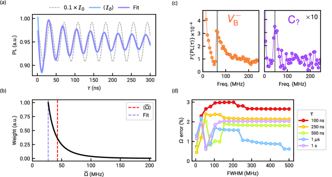
We undertake this Rabi measurement comparison with hBN flakes exfoliated directly onto a co-planar waveguide [Fig. S7(a,b)] to maximise the driving RF power. The out-of-plane magnetic field strength (provided by a permanent magnet) is tuned manually for the measurement on each defect type, to obtain a resonant frequency of 2.9 GHz in both cases [Fig. S7(c)]. For the defect () this corresponds to a field of 100 mT, and 20 mT for the defect (), avoiding anti-crossings and the cross-relaxation resonance. Rabi measurements are then undertaken at the respective fields at the same driving frequency [Fig. S7(d,e)]. Each column pair in (d,e) is a Rabi measurement at a given RF driving power (decreasing from left to right), for flakes 1 (d) and 2 (e). The flopping of the ensemble in each measurement can be immediately identified as slower than the ensemble, indicative of a lower spin multiplicity. We quantify this effect by fitting the Rabi measurement to an exponentially decayed cosine function with a free decay time, amplitude, frequency, phase and vertical offset. The free phase accounts for an average over detunings (see next section). The fit Rabi frequencies are displayed in main text Fig. 2(e), with the fit error estimated from a Monte-Carlo bootstrap method [49], added to a systematic error in field misalignment (see below). We will now address some alternative explanations for this difference, before ruling them out.
IV.3 Effect of detuning
The simple theory described in Sec. IV.1 assumed an idealised spin system with well defined transitions and no dephasing effects. In reality, the transitions have a finite linewidth (related to the spin dephasing time ) and may also encompass multiple hyperfine lines. The defect’s electron spin transition has a particularly large linewidth, with 7 hyperfine lines 47 MHz apart [1]. A finite linewidth implies that the RF driving is detuned from resonance most of the time, which may result in a faster apparent flopping rate.
To model this effect, we use the generalised equation for the Rabi curve in the presence of a detuning (in rad/s),
| (S9) |
where the generalised Rabi frequency reads
| (S10) |
Note that any increases with respect to the bare , as well as reducing the oscillation amplitude. We numerically model this generalised Rabi curve by averaging over a 200 MHz Lorentzian linewidth to approximately match the lineshape. The resultant generalised curve [Fig. S8(a) blue] has a reduced amplitude compared with the no-detuning curve [Fig. S8(a) grey dashed], as well as a phase offset and a decay envelope, due to the interference of different . Despite this averaging, a function consisting of a cosine function with a free phase, frequency, amplitude, and with an exponential decay envelope, fits the data well [Fig. S8(a) purple]. The similar flopping frequency (within 0.01%) between the simple and detuning-averaged curves is at first surprising, as the expected generalised Rabi frequency based on the calculated distribution is a factor of 1.6 higher [Fig. S8(b)]. The bias of the fit to larger amplitude components, however, ensures the zero-detuning component is fit. The Lorentzian-distributed generalised Rabi frequency components can also be seen in Fourier-transformed experimental curves [Fig. S8(c)], with a tail to the higher frequency components after an initial peak that lines up with the frequency estimated by the fit. Note that the tail for the defect is compressed, as it has a narrower () intrinsic linewidth than the .
The general Rabi curve shows a decay envelope from the averaging over detunings, where the model includes no additional decay envelope due to other dephasing effects. In Fig. S8(d) we explore the frequency estimation error as a function of characteristic decay times and ODMR lineshape widths (FWHM). Here the estimation error is defined as the relative error between the fit frequency and the input bare Rabi frequency . The estimation error is below 3% for all simulations, below the error estimated from the fit statistics and systematic field misalignments (see below).
IV.4 Effect of field misalignments
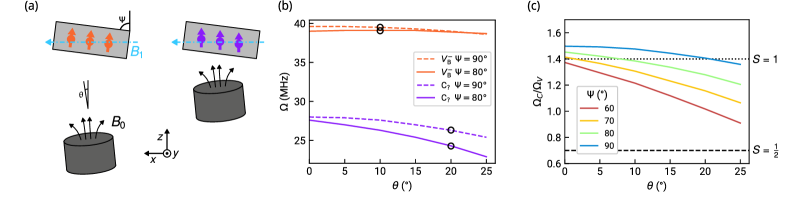
In Sec. IV.1 we assumed the static field to be exactly aligned with the intrinsic quantization axis of the defect (the -axis of the hBN crystal, which was assumed parallel to ), and the RF field to be exactly perpendicular to the -axis, as is nominally the case experimentally. Here we model the effect of misalignments away from these nominal conditions.
First, we consider the effect of a misalignment. The two Rabi experiments were undertaken with the same RF conditions (power, geometry), however the bias magnet was moved closer to the sample in for the measurement [Fig. S9(a)]. Figure S9(b) (dashed lines) plots the calculated Rabi frequency for the two defects as a function of the bias field’s polar angle (). The Rabi frequency scales with the projection of the RF driving field onto the defect’s quantization axis according to Eq. S3. Therefore, the Rabi frequency drops as the driving RF field becomes less orthogonal to the spin axis. As the zero-field splitting (ZFS) of the defect protects the spin sublevels from mixing, it maintains a higher orthogonality with the RF driving field and thus a higher Rabi frequency.
Next, we consider the effect of a (RF) misalignment, modelled as a tilt of the flake’s -axis relative to (angle ) in Fig. S9(a). We use a coplanar RF waveguide designed to provide an in-plane () above the central stripline, but the flake may form a small angle with the surface. From ODMR measurements on various flakes we estimate the crystal tilt/RF misalignment angle to be less than 10°. Figure S9(b) displays the bare Rabi frequency under this worst-case tilted-flake assumption, as a function of polar bias angle (solid lines). We assume an initial bias field misalignment for the measurement to be 10°, and then 20° misalignment for the measurement as the magnet is brought closer (from 10 cm to 1 cm). We estimate the relative error in Rabi frequency due to this field misalignment uncertainty for Fig. 2(e) in the main text from the percentage error between the solid and dashed lines in Fig. S9(b) at these bias field polar angles (annotated circles). This corresponds to a 10% maximum error for the case, well below what would be required to be compatible with the or scenarios.
To see how much misalignment would be required to make the defect look like a spin if it was in fact a spin for example, in Fig. S9(c) we model the experiment in Fig. S7 assuming the defect has and , and assume the worst-case field misalignment of 10° for the measurement, before varying the angle of misalignment of the defect, for various RF misalignments . With no misalignment, the Rabi frequency ratio is , but this ratio drops as misalignment is increased. To recover the ratio measured experimentally and expected for a spin , one would require to have a combination of unrealistically large misalignments, for instance 30° misalignment of the flake or RF field () and a bias field misalignment for the measurement. These angles are beyond our estimates for the systematic error in alignments so rule out a misaligned bias field as the cause of the Rabi frequency difference.
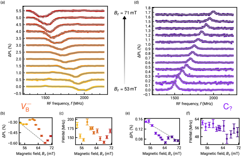
V Additional data for the cross-relaxation experiment
In the main text we displayed [Fig. 3(e)] a change in spin contrast at the CR condition. Here we plot the full dataset and explain the data normalisation and background subtraction procedure. An ODMR spectrum at each bias field strength for the pair of defects is shown in Fig. S10(a,d). These spectra are fit with a simple Lorentzian lineshape, and the resonance contrast [Fig. S10(b,e)] and linewidth [Fig. S10(c,f)] plot versus field. The contrast for both defects show a decrease in contrast magnitude with RF frequency, as a background to the CR resonance lineshape. We identify this background trend as being caused by an RF power spectrum variation, which we approximate with a linear slope [grey lines in Fig. S10(b,e)]. For the defects we estimate the linear slope with the first and the last point. In the case we do not include the two highest magnetic field points, identifying their decrease in contrast magnitude with the excited-state level anticrossing (ESLAC) at the nearby field of 76 mT [33]. To compare to a theoretical CR lineshape (see next section) we calculated the spin contrast as the magnitude of the ODMR resonance contrast, normalised to unity off-resonance after the background subtraction.
VI Modelling for the cross-relaxation experiment
In this section we model the expected spin contrast drop due to cross-relaxation between the two defect species measured in Fig. 3 of the main text. We will initially consider the measurement of the defect in a bath, before discussing the measurement. Broadly, we will determine the additional relaxation rate experienced by the spins as a function of detuning from the CR resonance condition, given the defect species’ dephasing rates, as an ensemble average over the probe-target (-) separation distance distribution. Given this cross-relaxation rate, we will model the spin contrast of the pulsed ODMR measurement, accounting for the effect of spin relaxation during the laser pulse as well as during the dark time .
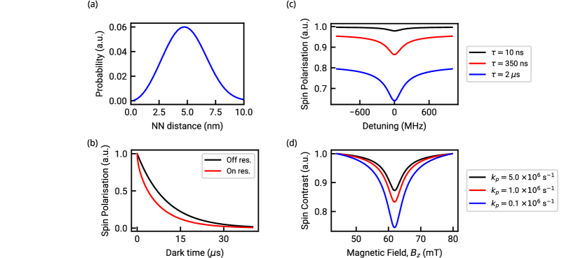
The probability distribution for the nearest-neighbour distance in a spin ensemble of density is [50]
| (S11) |
If we take to be the density of spins (), then for any given spin Eq. S11 also describes the distance of the spin (probe spin) to the nearest spin (target). As discussed in Sec. III.2 we estimate the density in our sample to be cm-3 [48]. The calculated nearest-neighbour distribution is shown in Fig. S11(a), peaked below 5 nm and with a significant population below 2 nm separation.
We will only consider the effect of the nearest (which is a good approximation for spin relaxation calculations [30]) but will average the results over the probability distribution Eq. S11 to model the measurement of an ensemble of spins. Thus, we only need to model a two-spin system, namely a - pair separated by a distance . Following Wood et al. [51], the additional relaxation rate due to cross-relaxation in the strong dephasing regime ( [30], justified later) is
| (S12) |
where is the dipole-dipole coupling strength, is the sum of the defect dephasing rates, and is the detuning from the CR resonance condition. is given by
| (S13) |
where GHz/T is the reduced gyromagnetic ratio (taken to be identical for and for simplicity), and is the angle between the quantization axis (magnetic field direction) and the - direction. The dephasing rate of each spin ensemble is related to the natural linewidth observed in a pulsed ODMR measurement [30]. We will take MHz and MHz, as determined for the sample considered.
The total relaxation rate experienced by the spin is then where is the background relaxation away for the CR resonance. We will take s which is a typical value for in our samples, see Fig. S6(d). Assuming perfect initialisation of the - pair in the interacting state, we can plot an ensemble-averaged relaxation curve of the spins [Fig. S11(b)], on and off resonance. We see that the effect of CR is felt even at short dark times s where the spin polarisation decays sharply. This sharp decay can be understood by considering the distance distribution, Fig. S11(a). At the most probable distance of 4.7 nm, the added relaxation rate on resonance (averaging over an isotropic angular distribution) is s-1, but this increases to s-1 at 2 nm distance, which is much larger than s-1 and causes some spins to relax over a time scale of ns. Note that the dipole-dipole coupling strength is MHz, much smaller than the dephasing rate of the coupled system ( MHz), which justifies the strong dephasing regime assumption.
If we now vary the detuning and calculate the remaining spin polarisation after a fixed dark time , we can construct a CR spectrum, shown in Fig. S11(c) for different values. We see that the CR resonance is pronounced even for a relatively modest ns, which is the value used experimentally, leading to a 10% contrast. A longer (e.g. 2 s) can double the contrast of the CR resonance, but this implies a longer measurement sequence which in practice does not lead to an improved signal-to-noise ratio.
Experimentally, to probe the spin polarisation we used a pulsed ODMR sequence comprised of a laser pulse of duration s, a dark time ns, and an RF -pulse. The laser pulse serves not only to read out the spin polarisation but also to re-set it to some initial value. However, at the CR resonance the relaxation rate is sufficiently high that it reduces the level of polarisation reached at the end of the laser pulse. Consequently, the ODMR contrast at the CR resonance is reduced even further.
To account for this effect, we modelled the spin dynamics during the entire pulsed ODMR sequence, following a similar treatment to Robertson et al. [19] (refer to equations S12-S19 of their paper). In brief, we consider a two-level model (the two spin states and of the defect) where the laser adds a rate driving the transition , while the relaxation rate is always on. The RF -pulse is assumed to instantly swap the two spin populations. The measured PL is related to the spin populations during the laser pulse, which allows us to derive an expression for the PL measured from the ODMR sequence with the -pulse (signal ) as well as the PL measured with the same sequence without the -pulse (reference ) which we use experimentally for normalisation. The ODMR contrast is defined as .
Using this model, we can compute the ODMR contrast () versus detuning () spectrum, and finally versus as presented in Fig. 3(e) of the main text. Additional simulated spectra are shown in Fig. S11(d) for different values of the pumping rate . As expected, the finite pumping rate enhances the contrast of the CR resonance, e.g. to 17% for s-1 and 25% for s-1, matching the experimentally observed contrast. We independently estimated the experimental value of to be in the range s-1 based on a separate measurement of as a function of following the analysis in Robertson et al. [19]. For the curve displayed in the main text, we assumed s-1.
To model the CR measurement with the ensemble as the probe, we apply the same model as described above except that at the CR resonance the spins are coupled with the entire bath of spins, which includes the defects but also other paramagnetic defects that are optically inactive. Since this density is a priori unknown, we leave it as a free parameter. All the other parameters are taken as above, except for the pumping rate which was determined to be s-1 [19]. We find a best fit to the data using cm-3.
VII Supplementary Information for the magnetic imaging experiments
VII.1 Magnetic imaging of CoFeB structures
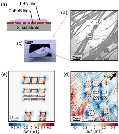
In Fig. 4 of the main text, we performed magnetic imaging of a CoFeB sample using the defects in hBN powder (Powder 2). The sample was made by etching rectangular structures using focused ion beam milling into an otherwise continuous film of CoFeB (5 nm thickness) sputtered onto a Si/SiO2 substrate and capped with 5 nm Ta [Fig. S12(a)]. The CoFeB film exhibits in-plane magnetization.
An optical micrograph of the CoFeB sample prior to depositing the hBN film [Fig. S12(b)] shows the etched rectangles as well as scratches that were made while cleaning the sample. Some of these scratches are deep enough to reach the CoFeB film and thus create additional magnetic features. The hBN powder film was prepared as described in Sec. II.1 and had an estimated thickness of a few microns. A photograph of the sample with the hBN film is shown in Fig. S12(c).
ODMR spectra were acquired in widefield which allowed us to form a magnetic field image [52]. The full magnetic image obtained is shown in Fig. S12(d), which is cropped for Fig. 3(b) of the main text. Comparing Fig. S12(d) with Fig. S12(b), we see that the magnetic field pattern correlates with the etched rectangles as well as some of the scratches. To compare the experimental image to simulations, we modelled the rectangular structures, ignoring the scratches. From a stray field point of view, an etched rectangle in an infinite magnetic film is equivalent to an isolated rectangular magnetized element, with a magnetization direction opposite to the film. Thus, we only need to simulate the stray field from a few rectangular elements.
The magnetization of the magnetic elements is assumed to be aligned with the external magnetic field (but pointing in the opposite direction as discussed above) with a magnitude A/m, which is a typical value for CoFeB. The stray field produced by each magnetic element at a distance above the film is computed using standard formulas given e.g. in Ref. [53]. The calculated vector field is then projected onto the measurement axis, which here corresponds to the direction of the applied static field since it sets the quantization axis of the defects. The resulting simulated image is shown in Fig. S12(e). For the standoff distance , we used m, which gives a good approximation for an hBN film of thickness m.
VII.2 Magnetic imaging of an Fe3GeTe2 crystal
In Fig. 5 of the main text, we performed a similar magnetic imaging experiment to Fig. 4 except that the magnetic sample here is a Fe3GeTe2 crystal and the experiments are done at K. The Fe3GeTe2 crystal imaged is a flake (estimated thickness of m) exfoliated from a larger crystal, the details of which can be found in Ref. [54]. The exfoliated flake was transferred onto a quartz coverslip placed on top of a coplanar waveguide for RF driving, and covered with an hBN film (Powder 2), see a photograph in Fig. S13(a).
Magnetic images near the edge of the Fe3GeTe2 flake were recorded with different directions of the external magnetic field (characterised by the tilt angle away from the -axis) as explained in the main text. Example ODMR spectra from the edge of the flake are shown in Fig. S13(b) for different values of . Bulk Fe3GeTe2 is a soft ferromagnet with an easy axis of magnetization along its -axis [35, 36]. Although thin flakes of Fe3GeTe2 can exhibit hard ferromagnetism [54], our relatively thick flake was found to exhibit no remanent magnetization and so can be modelled as a soft ferromagnet, characterised by magnetic susceptibility constants and , in response to a magnetic field applied parallel and perpendicular to the easy axis, respectively.
To compare the data to simulations, we model the flake as a soft rectangular magnetic element with magnetization vector where and are the out-of-plane and in-plane magnetization components, and the external magnetic field is . The stray field at a standoff m is computed and projected along the direction of the external field, and compared with the experiment. We first use the case where is applied in the -direction () to estimate by matching the simulation to the experiment. There is a large uncertainty on the value of because some parameters are not precisely known (thickness of the Fe3GeTe2 flake, thickness of the hBN film i.e. standoff ). However, once is fixed to match the data at , the effect of varying the angle should depend mainly on the ratio , independent on the exact value of . This ratio was adjusted to best fit the data, as shown in Fig. 3(d) of the main text. Simulated stray field vs angle curves for different ratios are shown in Fig. S13(c).
We note that in the particular geometry considered, the difference between and is small, although the latter case predicts a negative stray field at which we don’t see experimentally, confirming our sample has significant out-of-plane anisotropy. However, the measurement can be made much more sensitive to with a better optimised geometry. For instance, if the field is rotated in the plane instead of the plane so as to induce an in-plane magnetization perpendicular to the edge of the flake (instead of parallel to it), the resulting stray field will be much larger allowing us to probe more accurately. Moreover, small flakes that can be imaged entirely will also lead to more accurate estimations of and .