Si/SiGe QuBus for single electron information-processing devices with memory and micron-scale connectivity function
Abstract
The connectivity within single carrier information-processing devices requires transport and storage of single charge quanta. Our all-electrical Si/SiGe shuttle device, called quantum bus (QuBus), spans a length of 10 m and is operated by only six simply-tunable voltage pulses. It operates in conveyor-mode, i.e. the electron is adiabatically transported while confined to a moving QD. We introduce a characterization method, called shuttle-tomography, to benchmark the potential imperfections and local shuttle-fidelity of the QuBus. The fidelity of the single-electron shuttle across the full device and back (a total distance of 19 m) is . Using the QuBus, we position and detect up to 34 electrons and initialize a register of 34 quantum dots with arbitrarily chosen patterns of zero and single-electrons. The simple operation signals, compatibility with industry fabrication and low spin-environment-interaction in 28Si/SiGe, promises spin-conserving transport of spin qubits for quantum connectivity in quantum computing architectures.
Controlling local charge densities in a semiconductor by metallic gate-electrodes sets the foundation of modern nanoelectronics. Raising their density triggered quantum mechanical effects paving the way to various nanoelectronic devices operating with single charge quanta. Discrete charge states of quantum dots (QDs) are stored to process digital information [1] and the spin of individual electrons is used to encode quantum bits for quantum computing in semiconductors [2, 3]. The exchange of charge quanta between functional blocks such as charge-photon interfaces [4, 5, 6], quantum registers [7], spin manipulation zones [8], single charge detectors [9] and current standard devices [10] would lead to quantum devices with new functionalities.
For conventional electronics, wires transport currents or voltages over extended distances. In quantum technology, wires cannot transport individual charges, as disorder limits their localization length hardly exceeding 100 nm. In micron-sized quantum structures, the charging energy becomes impractically small for utilizing charge states with definite electron number. Here we present a device named quantum bus (QuBus) [11, 12], which can solve this fundamental difficulty and might provide the key for the required [13, 14] scale-up of quantum computing architectures [15, 16, 17, 18].
Single electron [19, 20] and spin-conserving electron [21] shuttling has previously been demonstrated employing surface acoustic waves in piezoelectric semiconductors. Shuttling in non-polar materials such as silicon, which is highly attractive for quantum computing with electron-spins [22, 23, 24, 25], becomes more involved, as the electron transport requires a series of top gates. This additional complexity comes with the benefit of electron acceleration and velocity control [26, 27, 28, 29, 30]. In particular, the conveyor-mode shuttling approach in Si/SiGe combines this advantage with predictable spin coherence during shuttling and the requirement for just four input signals independent from the length of the shuttle device [12]. High-fidelity short-range conveyor-mode charge and spin shuttling has been demonstrated [11, 31].
In this work, we all-electrically position and detect up to 34 electrons in a single-electron conveyor-mode QuBus in Si/SiGe. Despite its length of 10 m and more than 100 electrostatic gates, the QuBus can be controlled by only six input terminals with low voltage pulse complexity. We introduce a characterization method we call shuttle tomography to benchmark the local shuttle fidelity of the QuBus using a single electron as a probe. By composing elementary pulses, we can control and detect any single electron pattern filling a series of 34 QDs. The conveyor-mode shuttle approach opens up new possibilities for probing local potential disorder in a quantum well, detecting single electrons with high lateral resolution across a length of 10 m and boosting multi-electron control for scalable spin qubit quantum computation.
QuBus device and pulse segments
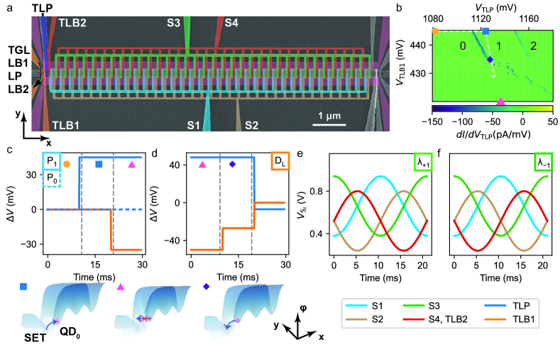
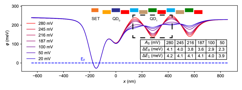
Our QuBus device consists of an undoped SiGe/Si/SiGe quantum well on top of which three electrically isolated metallic gate layers are fabricated by electron-beam lithography and metal lift-off (see the methods section for details on the device fabrication). The 10 m long grounded split-gate on the first layer defines a nominally depleted one-dimensional electron channel (1DEC) in the quantum well. More than 100 clavier gates, equally distributed among the second and third layer above the 1DEC, enable the approximately uniform movement of single electrons (conveyor-mode shuttling) along the x-direction (Fig. 1a). Notably, every forth clavier gate is electrically connected to one of four gate sets Si ().
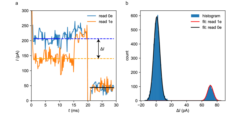
On demand, a single electron can be loaded into the 1DEC from the left single-electron transistor (SET) formed by the gates TGL, LB1, LP and LB2. The plunger gate TLP of the leftmost quantum dot QD0 controls the loading of exactly one electron from the SET to QD0. The corresponding voltage pulses in gate space are indicated in Fig. 1b from the yellow dot to the blue square. This is followed by raising the tunnel barrier by gate TLB1 (pink triangle in Fig. 1b,c). We label the corresponding pulse segment as P1. If the voltage applied to gate TLP remains low during the entire segment, no electron is loaded which we label as P0 (Fig. 1c). Reversely, we can also use the SET current to detect either zero or one electron in QD0 by the pulse segment (Fig. 1d). If an electron is detected, it is unloaded during the detection pulse (see Extended Data Fig. 1 for details on the charge detection).
To shuttle the single electron in a moving QD, simple sinusoidal voltage pulses are applied to the gate sets Si:
| (1) |
where the pulse amplitude sets the confinement strength of the propagating sinusoidal potential created in the 1DEC. and are constant offsets for accumulating charges in the conduction band in the 1DEC, accommodating different distances of the gate sets from the 1DEC. The shuttle velocity is given by ms-1, where the frequency of the shuttle pulse is Hz and nm is the lateral period of the potential in the 1DEC.
To transport all electrons in the 1DEC by a distance of in the positive (negative) x-direction, the pulse segment () is employed (Fig. 1e,f)). Note that all voltages applied to gates of the device return to their initial values at the end of each pulse segment. This implies that the correction of the SET’s operating point for capacitive cross-coupling to the clavier gate sets Si is constant and thus simple. The right SET and the rightmost clavier gates are not used here and voltages are chosen to have an open 1DEC towards an energetically lower lying electron reservoir. Hence, in total only six voltage pulses , and given by the elementary pulse segments P0, P1, , and control the whole 10 m long shuttle device, inside of which a total of 35 QDs (QDi with ) are formed along the 1DEC.
Single-charge shuttle tomography
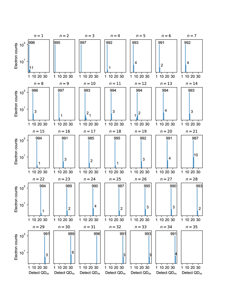
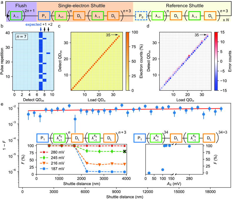
In order to discuss the composition and interplay of pulse segments during the operation of the QuBus, we choose the pulse sequence called shuttle tomography as a first example. The sequence is designed to measure the local shuttle fidelity , i.e. the shuttle success rate of for a specific position of the probe electron. Thus, we might identify local weak spots in the QuBus, although charge detection by the SET is limited to QD0. The strategy is to shuttle a single electron from the left end of 1DEC further into the 1DEC by some short distance and then back to the detector. We repeat this experiment in order to record the shuttle fidelity and sequentially increase the shuttle distance until the electron is shuttled the full distance of 19 m forth and back. The obtained data serves as a benchmark of the local shuttle fidelity in the QuBus. The corresponding pulse sequence is displayed in Fig. 2a. First, the depleted 1DEC is loaded with a single electron (P1) which is then shuttled into the 1DEC for a distance of (by repeating -times). Afterwards the electron filling of the first QDs is measured by consecutively detecting () and shuttling one period back towards the SET (). Finally, we apply a reference pulse by repeating the full pulse, but replace the P1 segment by P0. This shuttle pulse is -times repeated.
As an instructive subset of such a measurement over pulse repetitions with and mV, we observe the filling of each of the first eleven QDs as shown in Fig. 2b. During the majority of shuttle pulses the electron remains within QD7, into which it was loaded. This result indicates a well operating QuBus. Sometimes the electron is detected in QD8 and QD9, thus the shuttle process failed during these repetitions. Via the reference pulse segment, we check whether electrons leak into the 1DEC. Since we never observe any electrons during the reference pulse across thousands of repetitions for all , we conclude that there is no such leakage and the SET charge-detector does not faultily detect electrons in an empty QD.
The full observation of shuttle tomography with mV, and shows that the single electron is nearly always detected in the expected QDn, into which it has been loaded (Fig. 2c and Extended Data Fig. 2). Additionally, no electrons are observed for . This is expected as the right end of the 1DEC is open and the 1DEC only contains QD0 to QD34. Hence, the electron is pushed out of the 1DEC through its right end for .
We introduce the electron count to express the number of electrons detected in QDm summing over all pulse repetitions where is the expected filling of QD m, which is 1 only for and 0 otherwise. Thus, the error count of each QD relative to its expectation is given by . The single-electron error count (Fig. 2d) reveals that in very few repetitions the electron was detected in a QDm with and almost never for . In approximately 1 % of the repetitions the electrons seem to disappear () (see Extended Data Fig. 2). Remarkably, some electrons are detected in QD35 when loaded in QD34, although QD35 does not exist. Hence, delayed electrons got stuck during a pulse segment, instead of hopping over one QD during a pulse segment. This indicates a directionality of the shuttle error.
We define one shuttle pulse as successful, if three conditions are simultaneously fulfilled: (I) An electron is detected in the -th QD, into which an electron has been loaded. (II) No electron is detected in all other QDs, which are detected during the sequence. (III) No electron is detected during the reference shuttle sequence in any QD. We count the number of successful shuttle pulses with the same and divide by the total number of pulse repetitions to get the charge shuttle-fidelity .
With mV and for each of the covering a shuttle distance of nm, we observe an average shuttle infidelity of % (Fig. 2e). This infidelity, however, also includes errors from initialisation and detection pulse segments. Remarkably, is almost independent of the shuttle distance. Therefore, we split the observed infidelity into two error sources: First, the shuttle error occurring during each -pulse, which is a shuttle dependent error that accumulates over the increment of shuttle periods. Second, an electron loading and detection (LD) error , which is independent of shuttling and attributed to errors occurring during the P1 (no electron initialized by error) and (no electron detected by error) pulse segments. We linearly fit where and find the average shuttle fidelity per period at mV corresponding to an expected orbital splitting of 4 meV in (see Extended Data Fig. 3). The LD error is , thus the LD-corrected shuttle fidelity across the full channel and back is (total distance 19 m, see methods section for details on the estimations of errors).
Finally, we provoke shuttling errors by reducing and thus the confinement of the QDs in the shuttle potential. Note that the amplitude of the flush pulse is always constant at mV. We observe that as we decrease , the shuttle fidelity drops between the third and the forth shuttle period and then remains constant (left insert in Fig. 2e). Thus, we attribute the decrease in to a local weak spot in the QuBus potential, likely due to static potential disorder. To confirm this hypothesis, we modify the shuttling tomography pulse sequence by tuning as a function of shuttle distance. Therefore, temporarily enhanced confinement is realized by keeping mV during the fourth and the -th pulse segment, thus at the position of the weak spot only. This demonstrates a tunable method to shuttle electrons over the QuBus with high at much lower applied during all other pulse segments (right inset of Fig. 2e). The observed cut-off amplitude at mV matches well with simulations of semiconductor-oxide interface charge-defect induced potential disorder in the 1DEC [12]. The origin of the weak spot in the QuBus requires further investigation. Note that for the measurement of , we cannot fully exclude two errors appearing during shuttling which compensate each other. However, the observation that faulty shuttling behavior occurs locally in the QuBus, makes it probable that two such spots should be separately observed by the -dependence of the shuttling tomography.
Multi-electron operation
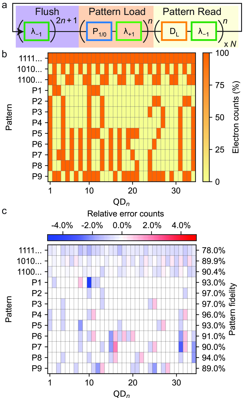
For the shuttle tomography, only exactly one electron was loaded into the QuBus at a time. The QuBus can also be operated with many electrons using the aforementioned elementary pulse segments. Each electron can be placed in any of the QDs between QD1 and QD34 in a controlled manner. Thus, we can create a pattern of electron fillings in a 34 QD register. The pulse sequence for loading and detecting an arbitrary electron pattern in the QuBus (Fig. 3a) is similar to the sequence employed during shuttle tomography. The repetition of segments is replaced by a series of single interleaved with P0 and P1 pulse segments. The latter determine the pattern filling the QDs. The key expectation is that any segment should move all electrons simultaneously by shifting the sinusoidal potential in the 1DEC.
Using mV, we load one electron in each of the 34 QDs (), every second QD () or a more complex periodic pattern (). We repeat the pattern loading and detecting for times to gather statistics on the electron count in each QD (Fig. 3b). We observe that the fraction of counted electrons in all QDs is very close to the expected filling pattern. Next, nine non-periodic patterns P1-P9, representing the lines of a binary image comprising bits, are successfully loaded and detected as observed from the statistics of pulse repetitions.
The dominant bluish color in the error-count map for all patterns (Fig. 3c) reveals that the main error is the apparent loss of electrons. We assign this notion to the dominance of the initialisation and detection error . It also explains why the pattern fidelity, which we define analogue to the shuttle-fidelity as the rate of successfully and exclusively placing and detecting electrons in all intended QDs, is lowest for the pattern with the highest electron count (111…). Blue/red dipoles in the error-count map indicate a shuttle error. As for shuttle tomography, we mainly observe individual electrons being misplaced by one QD to the right, provided this adjacent QD is nominally empty. This observation underlines the directional character of the shuttle error, which we already noted for the shuttle tomography.
Conclusion
Our all-electrical Si/SiGe electron-shuttle device is successfully operated in conveyor mode. Only six input terminals control the more than 100 clavier gates of the µm long device. Independent of its length, only four sinusoidal signals are required to operate the shuttle as well as two signals for loading and detecting electrons by a single-electron transistor. We introduce a method called shuttle tomography, which uses a single electron to probe the local shuttle fidelity and thus local imperfections in the confinement of the moving QD. We estimate the fidelity for shuttling one electron across the full length and back, thus a total distance of 19 m, to be . Employing other pulse sequences composed of the five elementary pulses for our QuBus, we programmatically distribute and detect up to 34 electrons across the 34 QDs formed in the shuttle device. Any QD filling pattern can be initialized and we encode a digital image, the pixels of which are represented by single electrons.
The QDs can be interpreted as a 34 bit stack with a maximum of 34 electrons or as the initialization procedure of a series of 34 QDs towards a quantum register for spin qubits. Preparing such patterns of electrons in a one-dimensional channel also opens up possibilities to study the interplay of tunnel coupling and Coulomb interaction for a specific charge configuration. Furthermore, our conveyor-mode QuBus device paves the way to scalable quantum computation, since it is expected that the electron-spin evolution is deterministic during conveyor-mode shuttling at a velocity of approximately 8 m s-1 and spin-coherent shuttle fidelities of 99.9 % are predicted [12]. Notably our QuBus is technologically compatible to industrial fabrication and Si/SiGe has been proven to be an ideal host-crystal for spin qubits. Spin-qubit connectivity across a distance of several micrometers could be a game changer for spin quantum computation.
Methods
The QuBus device
The undoped quantum well heterostructure is grown by chemical vapour deposition on a 200 mm silicon wafer and consists of a 7 nm tensile-strained silicon layer sandwiched between two relaxed layers of . The upper barrier layer of has a nominal thickness of 30 nm and is capped by 2 nm of Si. Ohmic contacts to the quantum well are created by the selective phosphorus ion-implantation followed by a rapid thermal anneal at for . The contacts are then metalized using optical lithography and metal lift-off. Three metallic gate layers including fan-out are fabricated via electron beam lithography and evaporation followed by metal lift-off. A scanning electron micrograph of a device nominally identical to the device measured in this work can be seen in Fig. 1a. The first gate layer is deposited directly onto the silicon capping layer, the native oxide layer of which was removed immediately before metal evaporation via HF etching. For this lowest layer of palladium is used in order to fabricate a suitable metal-semiconductor junction. The later two gate layers are fabricated on of atomic layer deposited and consist of of titanium and / of platinum for the second and third layer, respectively.
The first fine gate layer defines both the SET plunger and barrier gates as well as the channel-confining split-gate. The split-gate constrains the 1DEC to a width below . The second and third metal gate layers define the SET top gates as well as the clavier gates, which form the individual QDs in the 1DEC. These clavier gates have a width of with a pitch of . The designed distance between SET and QD0 and thus the tunnel-coupling is based on Ref. [32].
Experimental setup
Experiments are conducted in an Oxford Triton 200 dilution refrigerator at approximately mK. Voltage pulses are generated by a Zurich Instruments HDAWG8 and superposed with DC voltages from a home-built DAC by a passive voltage adder at room-temperature. All signal lines are filtered by pi-filters with a cut-off frequency of 1 kHz. No low-temperature filtering is used. The SET current is converted by the low-noise transimpedance amplifier SP983c from Basel Precision Instruments with a cut-off frequency of 3 kHz and digitized by an AlazarTech ATS9440 waveform digitizer. The composition of pulse sequences employs the open source python package qupulse [33].
Error Estimation
Here we discuss and estimate the error probability for manipulating the charge state during each elementary pulse segment with . First, we assume for simplicity that the average error for shuttling one electron by a distance of is despite the experimentally observed small directionality. Since we never observe any electrons during the reference pulse across thousands of shuttle tomography repetitions for all , we conclude that and that the detector does not faultily detect electrons in an empty QD. We combine the error from loading one electron and missing an electron during detection to be the loading and detection error with . The experimentally observed shuttle fidelity during a shuttle tomography pulse sequence of shuttle distance is composed of several elementary pulse segments:
By linearly fitting , we find and the average shuttle fidelity per period . Thus, the expected LD-corrected shuttle fidelity for a total shuttle distance of m is . This corresponds to the fidelity of shuttling a single electron across the full QuBus and back.
Acknowledgements
We thank Łukasz Cywiński for helpful comments on the manuscript. This work has been funded by the German Research Foundation (DFG) under Germany’s Excellence Strategy - Cluster of Excellence Matter and Light for Quantum Computing" (ML4Q) EXC 2004/1 - 390534769 and by the Federal Ministry of Education and Research under Contract No. FKZ: 13N14778. Project Si-QuBus received funding from the QuantERA ERA-NET Cofund in Quantum Technologies implemented within the European Union’s Horizon 2020 Program. The device fabrication has been done at HNF - Helmholtz Nano Facility, Research Center Juelich GmbH [34].
Author contributions
R.X. conducted the experiments with M.B and L.R.S. R.X. and M.B. analysed the data with I.S. and L.R.S. S.H. provided measurement software. T.S prepared the passive voltage adder. M.B. adapted the developed process by R.X, J.-S.T and I.S for the device fabrication and fabricated the device. S.T. operated e-beam lithography. L.R.S. designed the device and supervised the experiment. L.R.S and H.B. provided guidance to all authors. R.X., M.B. and L.R.S. wrote the manuscript, which was commented by all other authors.
Competing interests
R.X., I.S., H.B. and L.R.S. are co-inventors of patent applications that cover conveyor-mode shuttling and its applications. L.R.S. and H.B. are founders and shareholders of ARQUE Systems GmbH. The other authors declare no competing interests.
References
- Chen et al. [1996] R. H. Chen, A. N. Korotkov, and K. K. Likharev, Single-electron transistor logic, Appl. Phys. Lett. 68, 1954 (1996).
- Ono et al. [2005] Y. Ono, A. Fujiwara, K. Nishiguchi, H. Inokawa, and Y. Takahashi, Manipulation and detection of single electrons for future information processing, J. Appl. Phys. 97, 031101 (2005).
- Hanson et al. [2007] R. Hanson, L. P. Kouwenhoven, J. R. Petta, S. Tarucha, and L. M. K. Vandersypen, Spins in few-electron quantum dots, Rev. Mod. Phys. 79, 1217 (2007).
- Joecker et al. [2019] B. Joecker, P. Cerfontaine, F. Haupt, L. R. Schreiber, B. E. Kardynał, and H. Bluhm, Transfer of a quantum state from a photonic qubit to a gate-defined quantum dot, Phys. Rev. B 99, 205415 (2019).
- Arakawa and Holmes [2020] Y. Arakawa and M. J. Holmes, Progress in quantum-dot single photon sources for quantum information technologies: A broad spectrum overview, Appl. Phys. Rev. 7, 021309 (2020).
- Higginbottom et al. [2022] D. B. Higginbottom, A. T. K. Kurkjian, C. Chartrand, M. Kazemi, N. A. Brunelle, E. R. MacQuarrie, J. R. Klein, N. R. Lee-Hone, J. Stacho, M. Ruether, C. Bowness, L. Bergeron, A. DeAbreu, S. R. Harrigan, J. Kanaganayagam, D. W. Marsden, T. S. Richards, L. A. Stott, S. Roorda, K. J. Morse, M. L. W. Thewalt, and S. Simmons, Optical observation of single spins in silicon, Nature 607, 266 (2022).
- Volk et al. [2019] C. Volk, A. M. J. Zwerver, U. Mukhopadhyay, P. T. Eendebak, C. J. van Diepen, J. P. Dehollain, T. Hensgens, T. Fujita, C. Reichl, W. Wegscheider, and L. M. K. Vandersypen, Loading a quantum-dot based “qubyte” register, npj Quantum Inf 5, 29 (2019).
- Neumann and Schreiber [2015] R. Neumann and L. R. Schreiber, Simulation of micro-magnet stray-field dynamics for spin qubit manipulation, J. Appl. Phys. 117, 193903 (2015).
- Cassidy et al. [2007] M. C. Cassidy, A. S. Dzurak, R. G. Clark, K. D. Petersson, I. Farrer, D. A. Ritchie, and C. G. Smith, Single shot charge detection using a radio-frequency quantum point contact, Appl. Phys. Lett. 91, 222104 (2007).
- Stein et al. [2017] F. Stein, H. Scherer, T. Gerster, R. Behr, M. Götz, E. Pesel, C. Leicht, N. Ubbelohde, T. Weimann, K. Pierz, H. W. Schumacher, and F. Hohls, Robustness of single-electron pumps at sub-ppm current accuracy level, Metrologia 54, S1 (2017).
- Seidler et al. [2022] I. Seidler, T. Struck, R. Xue, N. Focke, S. Trellenkamp, H. Bluhm, and L. R. Schreiber, Conveyor-mode single-electron shuttling in Si/SiGe for a scalable quantum computing architecture, npj Quantum Inf 8, 100 (2022).
- Langrock et al. [2023] V. Langrock, J. A. Krzywda, N. Focke, I. Seidler, L. R. Schreiber, and L. Cywiński, Blueprint of a scalable spin qubit shuttle device for coherent mid-range qubit transfer in disordered Si/SiGe/SiO2, PRX Quantum 4, 020305 (2023).
- Fowler et al. [2012] A. G. Fowler, M. Mariantoni, J. M. Martinis, and A. N. Cleland, Surface codes: Towards practical large-scale quantum computation, Phys. Rev. A 86, 032324 (2012).
- Gidney and Ekerå [2021] C. Gidney and M. Ekerå, How to factor 2048 bit RSA integers in 8 hours using 20 million noisy qubits, Quantum 5, 433 (2021).
- Vandersypen et al. [2017] L. M. K. Vandersypen, H. Bluhm, J. S. Clarke, A. S. Dzurak, R. Ishihara, A. Morello, D. J. Reilly, L. R. Schreiber, and M. Veldhorst, Interfacing spin qubits in quantum dots and donors—hot, dense, and coherent, npj Quantum Inf 3, 34 (2017).
- Li et al. [2018] R. Li, L. Petit, D. P. Franke, J. P. Dehollain, J. Helsen, M. Steudtner, N. K. Thomas, Z. R. Yoscovits, K. J. Singh, S. Wehner, L. M. K. Vandersypen, J. S. Clarke, and M. Veldhorst, A crossbar network for silicon quantum dot qubits, Sci. Adv. 4, eaar3960 (2018).
- Boter et al. [2022] J. M. Boter, J. P. Dehollain, J. P. van Dijk, Y. Xu, T. Hensgens, R. Versluis, H. W. Naus, J. S. Clarke, M. Veldhorst, F. Sebastiano, and L. M. Vandersypen, Spiderweb array: A sparse spin-qubit array, Phys. Rev. Applied 18, 024053 (2022).
- Künne et al. [2023] M. Künne, A. Willmes, M. Oberländer, C. Gorjaew, J. D. Teske, H. Bhardwaj, M. Beer, E. Kammerloher, R. Otten, I. Seidler, R. Xue, L. R. Schreiber, and H. Bluhm, in preparation (2023).
- McNeil et al. [2011] R. P. G. McNeil, M. Kataoka, C. J. B. Ford, C. H. W. Barnes, D. Anderson, G. A. C. Jones, I. Farrer, and D. A. Ritchie, On-demand single-electron transfer between distant quantum dots, Nature 477, 439 (2011).
- Takada et al. [2019] S. Takada, H. Edlbauer, H. V. Lepage, J. Wang, P.-A. Mortemousque, G. Georgiou, C. H. W. Barnes, C. J. B. Ford, M. Yuan, P. V. Santos, X. Waintal, A. Ludwig, A. D. Wieck, M. Urdampilleta, T. Meunier, and C. Bäuerle, Sound-driven single-electron transfer in a circuit of coupled quantum rails, Nat Commun 10, 4557 (2019).
- Jadot et al. [2021] B. Jadot, P.-A. Mortemousque, E. Chanrion, V. Thiney, A. Ludwig, A. D. Wieck, M. Urdampilleta, C. Bäuerle, and T. Meunier, Distant spin entanglement via fast and coherent electron shuttling, Nature Nanotech 16, 570 (2021).
- Xue et al. [2022] X. Xue, M. Russ, N. Samkharadze, B. Undseth, A. Sammak, G. Scappucci, and L. M. K. Vandersypen, Quantum logic with spin qubits crossing the surface code threshold, Nature 601, 343 (2022).
- Noiri et al. [2022a] A. Noiri, K. Takeda, T. Nakajima, T. Kobayashi, A. Sammak, G. Scappucci, and S. Tarucha, Fast universal quantum gate above the fault-tolerance threshold in silicon, Nature 601, 338 (2022a).
- Philips et al. [2022] S. G. J. Philips, M. T. Mądzik, S. V. Amitonov, S. L. de Snoo, M. Russ, N. Kalhor, C. Volk, W. I. L. Lawrie, D. Brousse, L. Tryputen, B. P. Wuetz, A. Sammak, M. Veldhorst, G. Scappucci, and L. M. K. Vandersypen, Universal control of a six-qubit quantum processor in silicon, Nature 609, 919 (2022).
- Mills et al. [2022] A. R. Mills, C. R. Guinn, M. J. Gullans, A. J. Sigillito, M. M. Feldman, E. Nielsen, and J. R. Petta, Two-qubit silicon quantum processor with operation fidelity exceeding 99%, Sci. Adv. 8, eabn5130 (2022).
- Bertrand et al. [2016] B. Bertrand, S. Hermelin, S. Takada, M. Yamamoto, S. Tarucha, A. Ludwig, A. D. Wieck, C. Bäuerle, and T. Meunier, Fast spin information transfer between distant quantum dots using individual electrons, Nature Nanotech 11, 672 (2016).
- Mills et al. [2019] A. R. Mills, D. M. Zajac, M. J. Gullans, F. J. Schupp, T. M. Hazard, and J. R. Petta, Shuttling a single charge across a one-dimensional array of silicon quantum dots, Nat Commun 10, 1063 (2019).
- Noiri et al. [2022b] A. Noiri, K. Takeda, T. Nakajima, T. Kobayashi, A. Sammak, G. Scappucci, and S. Tarucha, A shuttling-based two-qubit logic gate for linking distant silicon quantum processors, Nat Commun 13, 5740 (2022b).
- Zwerver et al. [2022] A. M. J. Zwerver, S. V. Amitonov, S. L. de Snoo, M. T. Mądzik, M. Russ, A. Sammak, G. Scappucci, and L. M. K. Vandersypen, Shuttling an electron spin through a silicon quantum dot array (2022), arXiv:2209.00920 .
- Feng et al. [2023] M. Feng, J. Yoneda, W. Huang, Y. Su, T. Tanttu, C. H. Yang, J. D. Cifuentes, K. W. Chan, W. Gilbert, R. C. C. Leon, F. E. Hudson, K. M. Itoh, A. Laucht, A. S. Dzurak, and A. Saraiva, Control of dephasing in spin qubits during coherent transport in silicon, Phys. Rev. B 107, 085427 (2023).
- Struck et al. [2023] T. Struck, M. Volmer, L. Visser, T. Offermann, R. Xue, J.-S. Tu, S. Trellenkamp, H. Bluhm, and L. R. Schreiber, in preparation (2023).
- Klos et al. [2018] J. Klos, F. Hassler, P. Cerfontaine, H. Bluhm, and L. R. Schreiber, Calculation of tunnel couplings in open gate-defined disordered quantum dot systems, Phys. Rev. B 98, 155320 (2018).
- Humpohl et al. [2023] S. Humpohl, L. Prediger, P. Cerfontaine, P. Bethke, A. Willmes, M. Meyer, T. Hangleiter, E. Kammerloher, L. Lankes, T. Struck, P. Eendebak, and R. Xue, qutech/qupulse: Release 0.8 (2023).
- Albrecht et al. [2017] W. Albrecht, J. Moers, and B. Hermanns, HNF - Helmholtz Nano Facility, Journal of large-scale research facilities 3, A112 (2017).