single=true \DeclareAcronymte short = TE, long = transverse electric, foreign-plural = \DeclareAcronymtm short = TM, long = transverse magnetic, foreign-plural = \DeclareAcronymtod short = TOD, long = third order dispersion, foreign-plural = \DeclareAcronympcf short = PCF, long = photonic crystal fibre, foreign-plural = \DeclareAcronymsr-pcf short = SR-PCF, long = single-ring photonic crystal fibre, foreign-plural = \DeclareAcronymhcf short = HCF, long = hollow core fibre, foreign-plural = \DeclareAcronymwgm short = WGM, long = whispering gallery mode, foreign-plural = \DeclareAcronymnir short = NIR, long = near infrared, foreign-plural = \DeclareAcronymcd short = CD, long = core diameter, foreign-plural = \DeclareAcronymfft short = FFT, long = Fourier transform, foreign-plural = \DeclareAcronymod short = OD, long = outer diameter, foreign-plural = \DeclareAcronymsem short = SEM, long = scanning electron micrograph, foreign-plural = \DeclareAcronymrs short = RS, short-plural = , long = rotation stage, foreign-plural = \DeclareAcronymts short = TS, long = translation stage, foreign-plural = \DeclareAcronymmmf short = MMF, long = multimode fibre, foreign-plural = \DeclareAcronymzdw short = ZDW, long = zero dispersion wavelength, foreign-plural = \DeclareAcronymuv short = UV, long = ultraviolet, foreign-plural = \DeclareAcronymeuv short = EUV, long = extreme ultraviolet, foreign-plural = \DeclareAcronymmir short = mid-IR, long = mid-infrared, foreign-plural = \DeclareAcronymgvd short = GVD, long = group velocity dispersion, foreign-plural = \DeclareAcronymspm short = SPM, long = self-phase modulation, foreign-plural = \DeclareAcronymhhg short = HHG, long = high harmonic generation, foreign-plural = \DeclareAcronymarr-pcf short = ARR-PCF, long = anti-resonant-reflection photonic crystal fibres, foreign-plural = \DeclareAcronymPDMS short = PDMS, long = polydimethylsiloxane, foreign-plural = \DeclareAcronymMoO short = \textalpha-MoO3, long = \textalpha-molybdenum trioxide, foreign-plural = \DeclareAcronymVO short = \textalpha-V2O5, long = \textalpha-vanadium oxide, foreign-plural = \DeclareAcronymAFM short = AFM, long = atomic force microscopy, foreign-plural = \DeclareAcronymFTIR short = FTIR, long = Fourier transform infrared, foreign-plural = \DeclareAcronymMCT short = MCT, long = mercury cadmium telluride, foreign-plural = \DeclareAcronymTMM short = TMM, long = transfer matrix method, foreign-plural = \DeclareAcronymFP short = FP, long = Fabry–Pérot, foreign-plural = \DeclareAcronymTO short = TO, long = transverse optical, foreign-plural = \DeclareAcronymLO short = LO, long = longitudinal optical, foreign-plural = \DeclareAcronymER short = ER, long = extinction ratio, foreign-plural = \DeclareAcronymIL short = IL, long = insertion loss, foreign-plural = \DeclareAcronymvdW short = vdW, long = van der Waals, foreign-plural =
Deep-subwavelength Phase Retarders at Mid-Infrared
Frequencies
with van der Waals Flakes
Abstract
Phase retardation is a cornerstone of modern optics, yet, at \acmir frequencies, it remains a major challenge due to the scarcity of simultaneously transparent and birefringent crystals. Most materials resonantly absorb due to lattice vibrations occurring at \acmir frequencies, and natural birefringence is weak, calling for hundreds of microns to millimeters-thick phase retarders for sufficient polarization rotation. We demonstrate \acmir phase retardation with flakes of \acMoO that are more than ten times thinner than the operational wavelength, achieving degrees polarization rotation within one micrometer of material. We report conversion ratios above in reflection and transmission mode, and wavelength tunability by several micrometers. Our results showcase that exfoliated flakes of low-dimensional crystals can serve as a platform for \acmir miniaturized integrated polarization control.
I Introduction
From understanding the early universe [1] and mapping our galaxy [2] to encoding quantum information in photons [3], the polarization of an electromagnetic field is an important internal property of light. Controlling light’s polarization is also an indispensable part of modern life [4], spanning applications in sensing [5], imaging [6], microscopy [7], and telecommunications [8]. Phase retardation in particular, the process of introducing a phase difference between two orthogonal polarization states, is a crucial building block of modern optics. This phase difference is typically introduced by a phase retarder (or wave plate), which converts between linear and circular polarization and can achieve any elliptically polarized state in-between [9]. Despite the central role phase retardation plays in manipulating photons, for a large portion of the \acmir spectral range, namely at wavelengths above the central wavelength of the CO2 laser of , commercial wave plates are extremely scarce.
The lack of phase retardation schemes at mid-IR frequencies is an important roadblock in photonics, as this spectral range is fundamental to both science and technology, and currently experiencing rapid advancements [17]. Plank’s law of thermal radiation predicts a peak of thermal emission at wavelengths between for near-room temperatures, thus enabling a variety of light-harvesting applications including contactless temperature regulation, renewable energy [18, 19, 20], and thermal camouflage [21]. The \acmir range is also crucial in astronomy, for example \acmir polarimetry enables probing hot interstellar matter in our galaxy [22, 23]. Additionally, the earth’s atmosphere becomes transparent in this range, making \acmir night vision [24] and daytime radiative cooling [25] feasible and relevant, as well as paving the way for \acmir communications [26]. Molecular vibrations also occur in the \acmir range, thereby \acmir sensing [27], detection [28, 29], and medical microscopy [30] depend on controlling \acmir photons.
Like molecular vibrations, however, crystal lattice vibrations (phonons) in solids also occur at the mid-IR frequencies, yielding strong resonant absorption in all polar dielectrics. This greatly limits the range of available materials for polarization control elements and explains the technological gap in mid-IR phase retarders. In particular, for efficient phase retardation, transparent materials with strong intrinsic material birefringence, defined as , where and are the ordinary and extraordinary refractive indices of a uniaxial material, are required. Most materials that retain some degree of birefringence at \acmir frequencies resonantly absorb. Furthermore, birefringence is a weak effect and remains below unity () in bulk crystals, introducing major scalability challenges in integrated \acmir photonics. To understand this, let us consider the principle of operation of a phase retarder composed of a lossless uniaxial crystal. Its optimal thickness is given by:
| (1) |
where is the wavelength of operation. Eq. 1 gives the ideal thickness () for half-wave plate () or quarter-wave plate () operation, rotating linear polarization and converting it to circular polarization, respectively. To compensate for weak natural birefringence at \acmir frequencies, wave plates with thicknesses ranging from hundreds of microns to millimeters are required for sufficient phase retardation [31]. This is shown in LABEL:fig1:material-comparison, which presents a map of available birefringent materials that can operate as half-wave plates and the relevant spectral range within which they remain transparent.
Conventional materials like CaCO3 in the near-IR or AgGaSe2 in the mid-IR, shown in LABEL:fig1:material-comparison, ought to be hundreds of wavelengths thick to perform as half-wave plates and fall within the class of “optically thick” components (cyan highlighted region). The only available substitute for mid-IR wave plates are Fresnel rhomb retarders. These are even bulkier, approaching in size the centimeter-scale. To reduce size, one can engineer strong birefringence () for selected wavelengths using form birefringence, for example in liquid crystals [33, 34], or by design, using topology-optimized metasurfaces [35]. Nonetheless, these methods often require complex lithographic steps, and remain limited in their scalability. Reducing the dimensions of \acmir phase retardation schemes will resolve major practical challenges including mechanical instabilities, beam incoherence, overheating, thus enabling miniaturization for on-chip and integrated optics applications, where device compactness is required [36, 37].
In this article, instead of conventional phase retardation schemes with lossless anisotropic crystals, we consider a different class of materials as a platform for mid-IR phase retardation: \acvdW, low-dimensional, in-plane anisotropic, highly dispersive materials. Several low-dimensional materials, such as \acMoO [38, 39, 40] and \acVO [41], have been recently considered for their in-plane hyperbolic dispersion, leading to a plethora of intriguing phenomena. Examples include negative refraction [42, 43] and reflection [44], reversed Cherenkov radiation [45], and topological [46, 47], configurable and tunable [48, 43], steerable [49] phonon polaritons. By contrast, here, we utilize the hyperbolic response of \acMoO as an extreme case of birefringence to demonstrate a practical mechanism: phase retardation, for which a hyperbolic response is beneficial but not a requirement.
In particular, we measure experimentally the colossal resonant birefringence, approaching (LABEL:fig1:permittivity), owing to the ultra-long lifetimes of phonon polaritons in \acMoO along orthogonal crystallographic directions. This huge is ideal for polarization control, as Folland and Caldwell commented in 2018 [50]. By Eq. 1, in the lossless-limit, increasing birefringence can reduce the thickness of a phase retarder. Considering the measured birefringence of \acMoO and its frequency dispersion, we show in LABEL:fig1:material-comparison that it is placed near the top-left corner of the map (purple highlighted region), in the extreme sub-wavelength regime, where the notation “” and “” corresponds to a phonon resonance along the - and -crystal direction, respectively. This map shows that by leveraging the birefringence of \acMoO, the required thickness for sufficient phase retardation reduces by up to three orders of magnitude with respect to the operation wavelength, as compared to conventional bulk crystals. Recently, thin-film polarizers composed of \acMoO were demonstrated that reflect one linear polarization and dissipate the other [51]. Dereshgi et al. experimentally demonstrated a \acmir phase retarder employing \acMoO [52]; however these results pertain to heterostructure, requiring multiple steps of deposition and transfer. These devices, only working in reflection, exhibited high resonant absorption due to the optical phonons, and could only reflect a small portion () of the incoming light into the cross-polarized state.
In contrast, we probe experimentally the polarization rotation as well as the ellipticity of mid-IR photons, and showcase that single \acvdW flakes of anisotropic crystals suffice and can serve a practical material platform for miniaturized \acmir phase retardation in either reflection or transmission, with improved performance metrics. Despite the strong frequency dispersion and resonant absorption of \acMoO (LABEL:fig1:permittivityc) near the wavelength range of operation, insertion losses remain small due to the negligible thickness of the flakes as compared to the wavelength. With respect to the canvas of available materials, as a final remark, we note that a class of quasi one-dimensional chalcogenides has recently been introduced [16, 53], having birefringence comparable to \acMoO in the \acmir, as shown in LABEL:fig1:material-comparison for BaTiS3. Nonetheless, no phase retardation devices operating in the \acmir have been demonstrated so far, even with such material systems.
To our knowledge, our results mark the first reported phase retarders in the mid-IR above . Our results also demonstrate the thinnest reported phase retarders relative to the operation wavelength, for all spectral ranges. Finally, these do not require any lithography, thus reducing simultaneously design complexity and material volume with respect to existing phase retardation schemes. The concepts shown in this work with \acMoO for the sake of demonstration also apply to \acVO (see previous numerical results in [54]), which has the same type of anisotropy as \acMoO at larger wavelengths [41].
II Results
We mechanically exfoliate flakes of \acMoO from bulk crystals and transfer them to silicon and gold-coated glass substrates in order to realize phase retarders that operate in transmission and reflection mode, respectively. Exfoliated flakes of \acMoO typically possess a rectangular shape, due to the crystal’s orthorhombic structure [40] (LABEL:fig1:permittivitya). We refer to the crystal direction as the -axis, to the as the -axis, and to the direction as the -axis. We measure the dielectric permittivity of \acMoO using \acFTIR spectroscopy, implementing the method described in [32]. The results we obtain, shown in LABEL:fig1:permittivityb and LABEL:fig1:permittivityc, are in agreement with previous reports [38, 39, 40]. As shown in panel b, near , the dielectric function along the -axis () resonates due to a \acTO phonon occurring at the corresponding photon energy, while remains very small. Thus, the birefringence of \acMoO in this spectral region reaches values near 15.
Aiming to achieve degrees polarization rotation, we note that, while Eq. 1 appropriately describes the operation of optically thick and lossless dielectric wave plates, the class of \acvdW materials considered here requires taking into account their strong frequency dispersion due to phonon resonances as well as the non-negligible dichroism near-resonance. The latter makes orthogonal components of the electromagnetic fields experience different level of losses, whereas the former yields strong sensitivity to the optimal operational wavelength with respect to small changes in a flake’s thickness. Another important factor is the extremely small thickness of the phase retarders as compared to the wavelength. In this deeply subwavelength region, interference effects take precedence in describing the conversion process. It is thus essential to consider not only the phase acquired upon propagation within the slab, but also the reflection and transmission at its boundaries [55]. In the following sections, we utilize dichroism to effectively leverage constructive interference so that light maximally experiences the anisotropy of the crystal. Through a combination of simulations and experiments, we illustrate our approach to achieve significant polarization conversion while maintaining low insertion losses.
The topography of exfoliated flakes is characterized with \acAFM, while their spectral transmittance and reflectance is measured with \acFTIR micro-spectroscopy. To characterize the flakes, we control the input beam’s polarization and read the output beam’s polarization using two wire-grid polarizers, in both transmission and reflection modes, as shown in LABEL:fig2:setup and LABEL:fig3:setup, respectively. The input polarizer is oriented at with respect to the crystal’s axes, as shown with the blue straight line in the sketches next to the setup in LABEL:fig2:setup and LABEL:fig3:setup. This is a sketch of the polarization ellipse of the input beam with respect to the two crystallographic axes. As a result of the input polarizer, the input polarization ellipse reduces to a straight line, oriented at an angle of with respect to the -axis. Correspondingly, with the orange shape in the sketch next to the output polarizer in LABEL:fig2:setup and LABEL:fig3:setup, we represent a general elliptical polarization state with arbitrary ellipticity, defined by the quantity , with and being the half-lengths of the major and minor axes of the ellipse, respectively. For linearly polarized output light, the ellipse collapses into a line , whereas circularly polarized light traces a circle , corresponding to circular polarization. In the same schematics of LABEL:fig2:setup and LABEL:fig3:setup, we denote , which is the rotation angle of the principal axis of the output beam’s polarization ellipse, with respect to the input polarization, termed henceforth polarization rotation. In the case of a lossless dielectric crystal, the representation of a phase retarder via the pair (, ) reduces to the standard description via the retardance ( and correspond to a half-wave plate and quarter-wave plate operation, respectively), quoted in commercial wave plates.
We use simulations of reflectance and transmittance, performed using an in-house implementation of the \acTMM [56, 57], to estimate the optimal flake thickness for which the polarization rotation approaches degrees in the vicinity of , where birefringence is maximal. As shown in LABEL:fig2:trans-heatmap and LABEL:fig3:ref-heatmap, for both transmission and reflection, this occurs for thicknesses near . This thickness yields constructive interference within the flake, thus light maximally experiences the anisotropy of the crystal resulting in large linear polarization rotation while suppressing multiple reflections [58]. In transmission mode (LABEL:fig2:full), we define the polarization conversion ratio as and the phase retarder’s \acIL as , where and are the measured transmittance with the output polarizer perpendicular and parallel to the input one, respectively. Both and are normalized to , taken on the bare silicon substrate. In this notation, therefore, denotes the absolute conversion. LABEL:fig2:trans-spectrum shows the transmittance spectra measured for a flake of thickness (inset shows the \acAFM data). As can be seen from , maximum polarization rotation occurs at , and the absolute conversion is approximately .
Using the \acTMM, we show in LABEL:fig2:trans-heatmap a color map representing the calculated polarization conversion ratio as a function of flake’s thickness and wavelength. To gain a better understanding of the position of the maximum conversion ratio, we extract the ellipticity and the polarization rotation angle for each wavelength and thickness. The solid blue curve in LABEL:fig2:trans-heatmap shows the points where the output polarization is purely linear, meaning . Evidently, the maximum conversion ratio is achieved when along this line. The dashed black contours mark the areas where is within (inner contour line) and (outer contour line) from , hence the intersection between the blue curve and the dashed contours represents near-ideal quarter-wave plate operation. Experimental results are superimposed and shown as green dots, each corresponding to a particular flake with given thickness (-axis). The wavelength at which each measured data point is placed corresponds to the wavelength at which optimal polarization conversion (-axis) was measured. We observe good agreement between the experimental results and the solid line representing purely linear polarization (half-wave plate operation). Notably, three of our measurements, corresponding to three different flakes with different thicknesses, fall within a polarization rotation angle range between with high conversion ratios. From LABEL:fig2:trans-conversion, the maximum experimentally measured polarization conversion ratio is , and is achieved for for the wavelength of as shown by the vertical arrow. For all the experimental data points, the \acIL remains below . This was expected from the discussion above, owning to the deeply subwavelength thickness of the flakes, compensating for the large (LABEL:fig1:permittivityc).
We repeat the phase retardation characterization in reflection mode (LABEL:fig3:full), where and correspond to the output polarizer parallel and perpendicular to the input polarizer, respectively, as shown in LABEL:fig3:setup, normalized to the gold-coated substrate. We present in LABEL:fig3:ref-spectrum the measured reflectance spectra for a flake of thickness (\acAFM measurement in inset). For this flake, the maximum absolute conversion () is near . The maximum conversion is determined for each flake in the same manner as in transmission mode (LABEL:fig2:full), and varies for different flakes and different wavelengths depending on thickness. The green data points in LABEL:fig3:ref-heatmap represent these experimental results, and are superimposed with the corresponding \acTMM numerical calculations. The solid blue curve corresponds to pure linear polarization with . Unlike the transmission mode, in reflection mode, due to additional losses in the Au, the maximum predicted polarization rotation deviates from , as also verified experimentally (Fig. 5). The maximum polarization rotation angle predicted is . The regions where exceeds and are depicted by the inner and outer black dashed contour lines in white, respectively. The intersection between the blue curve and the dashed contours represents operation as close as possible to quarter-wave plate in reflection mode. Experimentally, although we do not expect maximal polarization rotation of , we still measure considerably high conversion ratio from one polarization state to its orthogonal counterpart. In reflection mode, light traverses the flake twice, thus experiencing the strong birefringence twice. This yields high conversion for a wider range of wavelengths than in transmission mode, as expected. This is shown in LABEL:fig3:ref-heatmap, where one can observe the potential to passively tune the operational wavelength and achieve linear polarization conversion by controlling the thickness of the flake within the range of . This enables operation within the wavelength range of , covering the entire Reststrahlen band of the \acMoO (LABEL:fig1:permittivityb), demonstrating that this effect does not stem from the hyperbolic behavior of \acMoO but rather from the resonant nature of its birefringence. Finally, as shown in LABEL:fig3:ref-conversion, we obtain conversion ratios up to , with \acIL remaining below for all measured flakes.
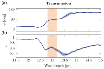
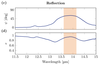
The results in LABEL:fig2:full and LABEL:fig3:full describe the intensity of the output beam’s component that is degrees rotated with respect to the input beam’s polarization. Nonetheless, these measurements do not suffice in characterizing a phase retarder. In particular in the case of considerable frequency dispersion and absorption (LABEL:fig1:permittivityb and LABEL:fig1:permittivityc), one ought to measure the ellipticity of the output beam, as linear polarization is not necessarily preserved. To do this explicitly (while probing depolarization and handedness), the mere use of two polarizers is insufficient, as one requires an additional phase retarder. Nonetheless, as mentioned in the introduction, commercial phase retarders are not available in the \acmir range. Hence, instead, following basic principles of ellipsometry [59], we illuminate the samples with linearly polarized light and measure the outgoing light in two configurations while rotating the sample: with the two linear polarizers parallel and orthogonal to each other. Assuming absence of depolarization, as expected in the deep-subwavelength range that these \acMoO flakes operate, via a numerical fit to the experimental data, we determine and as a function of the wavelength [60]. These are shown in Fig. 5b and Fig. 5d for transmission and reflection mode, respectively, whereas the corresponding ellipticity is shown in Fig. 5b and Fig. 5d.
As shown in Fig. 5b, in transmission mode, the polarization rotation angle reaches degrees for the spectral range from , as was initially designed. The ellipticity of the transmitted beam (Fig. 5b) deviates from the ideal value of unity for linear polarization, as expected due to losses. Nonetheless, this can be easily corrected with another polarization element on top of the flake or by directly etching a wire grid structure into the sample. In reflection mode, in Fig. 5d, we show that the rotation angle is approximately , as expected from our simulations shown in LABEL:fig3:ref-heatmap. In Fig. 5d the ellipticity of the reflected beam, however, is close to unity over the entire wavelength range for which it was designed, as highlighted in the orange shaded region from . This shows that linear polarization is preserved while being rotated. The deviations from the ideal behavior of a half-wave plate operation both both flakes operating in transmission and reflection mode are easilly corrected with polarizers that do exist in the mid-IR range.
III Discussion
We design and characterize a wide range of phase retarders composed solely by exfoliated flakes of \acMoO. By controlling the flakes’ thicknesses, we demonstrate polarization rotation in both transmission and reflection mode, with conversion ratios as high as . Phase retardation is demonstrated over the spectral range from , where bulk crystals perform poorly and commercial phase retarders are scarce. Due to the deeply subwavelength thickness of the flakes, the absorption of \acMoO does not considerably affect the performance of the phase retarders, and insertion losses remain extremely low. Nonetheless, the losses introduce a degree of circular polarization upon transmission, which, however, can be corrected by further adjusting the flakes’ thickness and using commercial polarizers.
Our experimental results demonstrate the potential of naturally in-plane anisotropic \acvdW materials as highly efficient phase retarders. This phase retardation is not associated with the hyperbolic dispersion of \acMoO, but rather the result of the resonant features in its dielectric permittivity due to crystal vibrations that occur at different frequencies along different lattice directions. Our results open new possibilities for practical applications in the \acmir spectral range, particularly beyond wavelengths of where conventional, where conventional bulk materials perform poorly. The principle of operation of the phase retardation scheme discussed in this work is general and applies to any polar dielectric low-dimensional anisotropic medium. Thus, these results can be generalized to other spectral ranges, where other materials exhibit Reststrahlen bands, for example near using \acVO [41] or even to \acMoO itself for the resonance along the -direction (see LABEL:fig1:material-comparison). As crystal growth techniques continue to improve, emerging \acvdW materials like \acMoO offer a new paradigm as polarization control elements, beyond the reach of conventional materials for integrated on-chip photonic devices.
IV Acknowledgments
This work is dedicated to the memory of John S. Papadakis. The authors declare no competing financial interest. The authors would like to thank V. Pruneri for generously granting access to his laboratory and equipment, as well as engaging in fruitful discussions. G.T.P. acknowledges financial support from the la Caixa Foundation (ID 100010434). M.E. acknowledges financial support from MCIN/AEI/ 10.13039/501100011033 (PRE2020-094401) and FSE “El FSE invierte en tu futuro”. M. G. acknowledges financial support from the Severo Ochoa Excellence Fellowship. This work was supported by the Spanish MICINN (PID2021-125441OA-I00, PID2020–112625GB-I00, and CEX2019-000910- S), the European Union (fellowship LCF/BQ/PI21/11830019 under the Marie Skłodowska-Curie Grant Agreement No. 847648), Generalitat de Catalunya (2021 SGR 01443) through the CERCA program, Fundació Cellex, and Fundació Mir-Puig. F.H.L.K. acknowledges support from the ERC TOPONANOP (726001), the government of Spain (PID2019-106875GB-I00) and Generalitat de Catalunya (CERCA, AGAUR, 2021 SGR 01443). Furthermore, the research leading to these results has received funding from the European Union’s Horizon 2020 under grant agreement no. 881603 (Graphene flagship Core3) and 820378 (Quantum flagship).
References
- Kamionkowski and Kovetz [2016] M. Kamionkowski and E. D. Kovetz, Annual Review of Astronomy and Astrophysics 54, 227 (2016).
- Hu and Lazarian [2023] Y. Hu and A. Lazarian, Monthly Notices of the Royal Astronomical Society 519, 3736 (2023).
- Zhang et al. [2008] Q. Zhang, X.-H. Bao, C.-Y. Lu, X.-Q. Zhou, T. Yang, T. Rudolph, and J.-W. Pan, Physical Review A 77, 062316 (2008).
- Ding et al. [2021] F. Ding, S. Tang, and S. I. Bozhevolnyi, Advanced Photonics Research 2, 2000173 (2021).
- Lee et al. [2023] G. H. Lee, H. Kang, J. W. Chung, Y. Lee, H. Yoo, S. Jeong, H. Cho, J.-Y. Kim, S.-G. Kang, J. Y. Jung, S. G. Hahm, J. Lee, I.-J. Jeong, M. Park, G. Park, I. H. Yun, J. Y. Kim, Y. Hong, Y. Yun, S.-H. Kim, and B. K. Choi, Science Advances 8, eabm3622 (2023).
- Zhou et al. [2022] S. Zhou, J. Bian, P. Chen, M. Xie, J. Chao, W. Hu, Y. Lu, and W. Zhang, Light: Science & Applications 11, 64 (2022).
- Intaravanne et al. [2022] Y. Intaravanne, R. Wang, H. Ahmed, Y. Ming, Y. Zheng, Z.-K. Zhou, Z. Li, S. Chen, S. Zhang, and X. Chen, Light: Science & Applications 11, 302 (2022).
- Wang et al. [2022] H. L. Wang, H. F. Ma, and T. J. Cui, Advanced Science 9, 2204333 (2022).
- Yariv and Yeh [1983] A. Yariv and P. Yeh, Optical waves in crystal propagation and control of laser radiation (Wiley, 1983).
- Dodge [1984] M. J. Dodge, Applied Optics 23, 1980 (1984).
- Ghosh [1999] G. Ghosh, Optics Communications 163, 95 (1999).
- Lisitsa et al. [1969] M. P. Lisitsa, L. F. Gudymenko, V. N. Malinko, and S. F. Terekhova, physica status solidi (b) 31, 389 (1969).
- Kato et al. [2021] K. Kato, K. Miyata, and V. Petrov, Applied Optics 60, 805 (2021).
- Kato and Shirahata [1996] K. K. K. Kato and H. S. H. Shirahata, Japanese Journal of Applied Physics 35, 4645 (1996).
- Tamošauskas et al. [2018] G. Tamošauskas, G. Beresnevičius, D. Gadonas, and A. Dubietis, Optical Materials Express 8, 1410 (2018).
- Niu et al. [2018] S. Niu, G. Joe, H. Zhao, Y. Zhou, T. Orvis, H. Huyan, J. Salman, K. Mahalingam, B. Urwin, J. Wu, Y. Liu, T. E. Tiwald, S. B. Cronin, B. M. Howe, M. Mecklenburg, R. Haiges, D. J. Singh, H. Wang, M. A. Kats, and J. Ravichandran, Nature Photonics 12, 392 (2018).
- Caldwell and Novoselov [2015] J. D. Caldwell and K. S. Novoselov, Nature Materials 14, 364 (2015).
- Datas and Vaillon [2019] A. Datas and R. Vaillon, Nano Energy 61, 10 (2019).
- Papadakis et al. [2021] G. T. Papadakis, M. Orenstein, E. Yablonovitch, and S. Fan, Physical Review Applied 16, 64063 (2021).
- Xiao et al. [2022] Y. Xiao, M. A. Kats, J.-J. Greffet, Q. Li, and G. T. Papadakis, Optical Materials Express 12, 1450 (2022).
- Zhu et al. [2020] H. Zhu, Q. Li, C. Zheng, Y. Hong, Z. Xu, H. Wang, W. Shen, S. Kaur, P. Ghosh, and M. Qiu, Light: Science & Applications 9, 60 (2020).
- Draine and Hensley [2021] B. T. Draine and B. S. Hensley, The Astrophysical Journal 909, 94 (2021).
- Packham et al. [2008] C. Packham, M. Escuti, G. Boreman, I. Quijano, J. C. Ginn, B. Franklin, D. J. Axon, J. H. Hough, T. J. Jones, P. F. Roche, M. Tamura, C. M. Telesco, N. Levenson, J. M. Rodgers, and J. P. McGuire, in Proc.SPIE, Vol. 7014 (2008) p. 70142H.
- Konstantatos [2018] G. Konstantatos, Nature Communications 9, 5266 (2018).
- Raman et al. [2014] A. P. Raman, M. A. Anoma, L. Zhu, E. Rephaeli, and S. Fan, Nature 515, 540 (2014).
- Zou et al. [2022] K. Zou, K. Pang, H. Song, J. Fan, Z. Zhao, H. Song, R. Zhang, H. Zhou, A. Minoofar, C. Liu, X. Su, N. Hu, A. McClung, M. Torfeh, A. Arbabi, M. Tur, and A. E. Willner, Nature Communications 13, 7662 (2022).
- Bareza et al. [2022] N. J. Bareza, B. Paulillo, T. M. Slipchenko, M. Autore, I. Dolado, S. Liu, J. H. Edgar, S. Vélez, L. Martín-Moreno, R. Hillenbrand, and V. Pruneri, ACS Photonics 9, 34 (2022).
- Huo et al. [2017] N. Huo, S. Gupta, and G. Konstantatos, Advanced Materials 29, 1606576 (2017).
- Wang et al. [2023] F. Wang, F. Hu, M. Dai, S. Zhu, F. Sun, R. Duan, C. Wang, J. Han, W. Deng, W. Chen, M. Ye, S. Han, B. Qiang, Y. Jin, Y. Chua, N. Chi, S. Yu, D. Nam, S. H. Chae, Z. Liu, and Q. J. Wang, Nature Communications 14, 1938 (2023).
- Kviatkovsky et al. [2020] I. Kviatkovsky, H. M. Chrzanowski, E. G. Avery, H. Bartolomaeus, and S. Ramelow, Science Advances 6, eabd0264 (2020).
- Dai et al. [2022] M. Dai, C. Wang, B. Qiang, F. Wang, M. Ye, S. Han, Y. Luo, and Q. J. Wang, Nature Communications 13, 4560 (2022).
- Sarkar et al. [2023] M. Sarkar, M. T. Enders, M. Shokooh-Saremi, K. Watanabe, T. Taniguchi, H. H. Sheinfux, F. H. L. Koppens, and G. T. Papadakis, Retrieving optical parameters of emerging van der Waals flakes (2023), arxiv:2305.13994 [physics.optics] .
- Marco et al. [2021] D. Marco, G. López-Morales, M. d. M. Sánchez-López, Á. Lizana, I. Moreno, and J. Campos, Scientific Reports 11, 9415 (2021).
- Herman and Kula [2017] J. Herman and P. Kula, Liquid Crystals 44, 1462 (2017).
- Shi et al. [2023] Z. Shi, A. Y. Zhu, Z. Li, Y.-W. Huang, W. T. Chen, C.-W. Qiu, and F. Capasso, Science Advances 6, eaba3367 (2023).
- Lin et al. [2022] Z. Lin, Y. Lin, H. Li, M. Xu, M. He, W. Ke, H. Tan, Y. Han, Z. Li, D. Wang, X. S. Yao, S. Fu, S. Yu, and X. Cai, Light: Science & Applications 11, 93 (2022).
- Zhou et al. [2019] H. Zhou, Y. Zhao, Y. Wei, F. Li, J. Dong, and X. Zhang, Nanophotonics 8, 2257 (2019).
- Ma et al. [2018] W. Ma, P. Alonso-González, S. Li, A. Y. Nikitin, J. Yuan, J. Martín-Sánchez, J. Taboada-Gutiérrez, I. Amenabar, P. Li, S. Vélez, C. Tollan, Z. Dai, Y. Zhang, S. Sriram, K. Kalantar-Zadeh, S.-T. Lee, R. Hillenbrand, and Q. Bao, Nature 562, 557 (2018).
- Zheng et al. [2018] Z. Zheng, J. Chen, Y. Wang, X. Wang, X. Chen, P. Liu, J. Xu, W. Xie, H. Chen, S. Deng, and N. Xu, Advanced Materials 30, 1705318 (2018).
- Álvarez-Pérez et al. [2020] G. Álvarez-Pérez, T. G. Folland, I. Errea, J. Taboada-Gutiérrez, J. Duan, J. Martín-Sánchez, A. I. F. Tresguerres-Mata, J. R. Matson, A. Bylinkin, M. He, W. Ma, Q. Bao, J. I. Martín, J. D. Caldwell, A. Y. Nikitin, and P. Alonso-González, Advanced Materials 32, 1908176 (2020).
- Taboada-Gutiérrez et al. [2020] J. Taboada-Gutiérrez, G. Álvarez-Pérez, J. Duan, W. Ma, K. Crowley, I. Prieto, A. Bylinkin, M. Autore, H. Volkova, K. Kimura, T. Kimura, M.-H. Berger, S. Li, Q. Bao, X. P. A. Gao, I. Errea, A. Y. Nikitin, R. Hillenbrand, J. Martín-Sánchez, and P. Alonso-González, Nature Materials 19, 964 (2020).
- Sternbach et al. [2023] A. J. Sternbach, S. L. Moore, A. Rikhter, S. Zhang, R. Jing, Y. Shao, B. S. Y. Kim, S. Xu, S. Liu, J. H. Edgar, A. Rubio, C. Dean, J. Hone, M. M. Fogler, and D. N. Basov, Science 10.1126/science.adf1065 (2023).
- Hu et al. [2023] H. Hu, N. Chen, H. Teng, R. Yu, M. Xue, K. Chen, Y. Xiao, Y. Qu, D. Hu, J. Chen, Z. Sun, and P. Li, Science 10.1126/science.adf1251 (2023).
- Álvarez-Pérez et al. [2022] G. Álvarez-Pérez, J. Duan, J. Taboada-Gutiérrez, Q. Ou, E. Nikulina, S. Liu, J. H. Edgar, Q. Bao, V. Giannini, R. Hillenbrand, J. Martín-Sánchez, A. Y. Nikitin, and P. Alonso-González, Science Advances 8, eabp8486 (2022).
- Guo et al. [2023] X. Guo, C. Wu, S. Zhang, D. Hu, S. Zhang, Q. Jiang, X. Dai, Y. Duan, X. Yang, Z. Sun, S. Zhang, H. Xu, and Q. Dai, Nature Communications 14, 2532 (2023).
- Hu et al. [2020] G. Hu, Q. Ou, G. Si, Y. Wu, J. Wu, Z. Dai, A. Krasnok, Y. Mazor, Q. Zhang, Q. Bao, C.-W. Qiu, and A. Alù, Nature 582, 209 (2020).
- Duan et al. [2021] J. Duan, G. Álvarez-Pérez, K. V. Voronin, I. Prieto, J. Taboada-Gutiérrez, V. S. Volkov, J. Martín-Sánchez, A. Y. Nikitin, and P. Alonso-González, Science Advances 7, eabf2690 (2021).
- Chen et al. [2020] M. Chen, X. Lin, T. H. Dinh, Z. Zheng, J. Shen, Q. Ma, H. Chen, P. Jarillo-Herrero, and S. Dai, Nature Materials 19, 1307 (2020).
- Dai et al. [2020] Z. Dai, G. Hu, G. Si, Q. Ou, Q. Zhang, S. Balendhran, F. Rahman, B. Y. Zhang, J. Z. Ou, G. Li, A. Alù, C.-W. Qiu, and Q. Bao, Nature Communications 11, 6086 (2020).
- Folland and Caldwell [2018] T. G. Folland and J. D. Caldwell, Nature 562, 499 (2018).
- Sahoo et al. [2022] N. R. Sahoo, S. Dixit, A. K. Singh, S. H. Nam, N. X. Fang, and A. Kumar, Advanced Optical Materials 10, 2101919 (2022).
- Dereshgi et al. [2020] S. A. Dereshgi, T. G. Folland, A. A. Murthy, X. Song, I. Tanriover, V. P. Dravid, J. D. Caldwell, and K. Aydin, Nature Communications 11, 9 (2020).
- Mei et al. [2023] H. Mei, G. Ren, B. Zhao, J. Salman, G. Y. Jung, H. Chen, S. Singh, A. S. Thind, J. Cavin, J. A. Hachtel, M. Chi, S. Niu, G. Joe, C. Wan, N. Settineri, S. J. Teat, B. C. Chakoumakos, J. Ravichandran, R. Mishra, and M. A. Kats, Colossal optical anisotropy from atomic-scale modulations (2023), arxiv:2303.00041 [physics.optics] .
- Dixit et al. [2021] S. Dixit, N. R. Sahoo, A. Mall, and A. Kumar, Scientific Reports 11, 6612 (2021).
- Holmes [1964] D. A. Holmes, JOSA 54, 1115 (1964).
- Passler and Paarmann [2017] N. C. Passler and A. Paarmann, Journal of the Optical Society of America B 34, 2128 (2017).
- [57] M. T. Enders, GeneralizedTransferMatrixMethod.jl.
- Pietraszkiewicz et al. [1995] K. Pietraszkiewicz, W. A. Woźniak, and P. Kurzynowski, Journal of the Optical Society of America A 12, 420 (1995).
- Tompkins and Irene [2005] H. Tompkins and E. A. Irene, Handbook of ellipsometry (William Andrew, 2005).
- Kilchoer et al. [2019] C. Kilchoer, N. Abdollahi, U. Steiner, I. Gunkel, and B. D. Wilts, APL Photonics 4, 126107 (2019).