.tifpng.pngconvert #1 \OutputFile \AppendGraphicsExtensions.tif
MoRe Electrodes with 10-nm Nanogaps for Electrical Contact to Atomically Precise Graphene Nanoribbons
Abstract
Atomically precise graphene nanoribbons (GNRs) are predicted to exhibit exceptional edge-related properties, such as localized edge states, spin polarization, and half-metallicity. However, the absence of low-resistance nano-scale electrical contacts to the GNRs hinders harnessing their properties in field-effect transistors. In this paper, we make electrical contact with 9-atom-wide armchair GNRs using superconducting alloy MoRe as well as Pd (as a reference), which are two of the metals providing low-resistance contacts to carbon nanotubes. We take a step towards contacting a single GNR by fabrication of electrodes with a needle-like geometry, with about 20 nm tip diameter and nm separation. To preserve the nano-scale geometry of the contacts, we develop a PMMA-assisted technique to transfer the GNRs onto the pre-patterned electrodes. Our device characterizations as a function of bias-voltage and temperature, show a thermally-activated gate-tunable conductance in the GNR-MoRe-based transistors.
keywords:
Graphene nanoribbons; Electronic properties; Substrate transfer; Field effect transistor; Metal-semiconductor contacts; Superconducting electrodes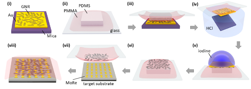
Introduction
Graphene nanoribbons (GNRs) are a quasi-1D analogue of graphene. Although graphene is classified as a 2D semimetal, a combination of quantum confinement and electron-electron interactions make GNRs semiconducting 1, 2, 3. The electronic band gap of GNRs scales inversely with their width and depends on their edge structure 2. This tunable band gap is a property that is of interest for field-effect transistors (FETs) 4, 5 and optoelectronics 6. Moreover, GNRs exhibit edges and ends that can host localized spin-polarized states 1, 7, 8 which is interesting for spintronic applications. Since the electronic properties of GNRs are sensitive to their width and edge structure, edge disorder and width variation at the atomic level result in hopping transport within the ribbon 9, which significantly suppresses their intrinsic electronic/spintronic properties 10.
On-surface, bottom-up chemical approaches have enabled the synthesis of a variety of GNRs from molecular precursors with structural precision on the atomic level 11, such as armchair 11, zigzag 12, chevron 11, staggered/topological 13, 14, metallic 15 and substitutionally doped GNRs 16. The electronic properties of these GNRs have mostly been studied by scanning tunneling microscopy. Characterization of the intrinsic electronic properties of the GNRs in electronic circuits has been comparatively limited by high contact resistances, limited chemical stability of the edges, and short GNR length below typical source-drain contact distances.
Low-resistance Ohmic electrical contacts are important for obtaining large on-state currents in FET devices, as well as for studying the intrinsic transport properties of GNRs. However, making consistent, low-resistance electrical contact to atomically-precise GNRs is challenging due to their on-surface synthesis with typical 1-nm width that leads to large band gaps (of the order or eV). Their typical length scale also results in a small contact area, of the order of . Recently, there have been considerable efforts to electrically contact atomically precise armchair-edge GNRs by electrodes made of graphene 17, 18, 19, 20, carbon nanotubes(CNTs) 21, palladium 5, 22, 23, 24 and gold 25. These studies, however, are still limited compared to the detailed characterization of a large variety of contacts to CNTs 26, 27. Even though CNTs structurally differ from GNRs by the absence of edges, small diameter (less than nm) CNTs are the closest system to atomically precise GNRs due to their similar band structure and considerable band gap (larger than eV) 28.
For the case of semiconducting CNTs, Schottky barriers are formed at the metal-CNT interfaces, the size of which depends on the chosen contact metal and the diameter of the nanotube. The presence of Schottky barriers results in a contact resistance that increases as the temperature is decreased. For CNTs, a distinction is often made between physisorption and chemisorption 29, 30, as well as p-type (high work function) and n-type (low work function) electrical contacts 27. Typically, n-type contacts form with metals that are prone to oxidation (Al, Sc, Y, Ti), while p-type contacts can be made with noble metals (Au, Pt, Pd), as well as Ni, Co, Mo and W.
Two of the metals that stand out for making low-resistance electrical contacts with small or absent Schottky barriers to CNTs are Pd 31, 32 and Mo 33/MoRe alloy 34, 35. Pd contacts to 9- and 13-atom-wide armchair GNRs (9-AGNRs and 13-AGNRs) have already been studied in a short-channel FET geometry by Llinas et al. 5, who found that transport in their devices was limited by tunneling through a Schottky barrier at the contacts. Nevertheless, their Pd-contacted 9-AGNR FETs with a HfO2 gate dielectric have a large on-state current ( A), as well as an on-off ratio of . Mo/MoRe on the other hand is of interest as it is a superconducting metal, which may be used to induce superconductivity in GNRs by the superconducting proximity effect 36 at cryogenic temperatures. In a weakly transparent electrical contact, the superconducting energy gap can be used to perform tunneling spectroscopy of the GNRs, while a highly transparent contact would allow for utilizing GNRs in Josephson junctions.
Here, we further explore MoRe and Pd contacts to 9-AGNRs by studying their current-voltage characteristics at various temperatures. In particular, we compare two distinct electrode geometries that have the potential to respectively address many GNRs in parallel, and single GNRs. With the aim of contacting single 9-AGNRs, an electrode design was made that minimizes gap width. Here we fabricate needle-like MoRe and Pd nanogap electrodes with a minimum width of nm and spacing of 6-15 nm. The smaller gap spacing achieved for this geometry could also enable addressing shorter GNRs. The polymer-free transfer method was attempted on this geometry, resulting in broken MoRe nanowires due to etching. In order to preserve the more fragile needle-like nanogaps and the contact geometry from etchants used in polymer-free GNR-transfer recipes, here we develop a PMMA-membrane-assisted technique for the transfer of the 9-AGNR films, based on the PMMA fishing transfer technique introduced by Martini et al. 17. This technique keeps the electrodes intact by preventing direct contact with any liquid and allows for controlled handling and m precise placement of the GNRs onto the electrical contacts using micro-manipulators. Our transfer method offers the additional advantage of using a stretched and clamped PMMA film, which could reduce wrinkling and folding. With this technique, we fabricate 10-nm nanogap MoRe and Pd devices and we investigate and compare their performance. We show that the 10-nm Pd nanogap devices have a few orders of magnitude higher conductance, which suggests that a Pd/MoRe bilayer thin film would be a better contact material for the realization of functional superconducting GNR devices.
Results
The 9-AGNRs were grown by on-surface synthesis37, discussed in detail in the methods section. The average length of the 9-AGNRs used in this work is 45 nm.
The two distinct electrode geometries used here to address the GNRs are the wide-nanogap and needle-like geometries. The wide-nanogap geometry consists of a pair of m long parallel wires, separated by approximately 30 nm. This geometry was made to address transport through many GNRs in parallel. The needle-like nanogap geometry consists of two opposing nanowires that are cuspated at a 30∘ angle, separated by less than 15 nm. This geometry minimizes the contact area and thus, increases the chance of making contact with a single GNR. The fabrication of these two electrode geometries is discussed in detail in the methods section.
Prior to the GNR transfer, the nanogap electrodes were characterized by recording the current versus bias voltage ( characteristic) in the bias range of -1 to 1 V. Only devices that were found to be electrically open (resistance 1 T at 1 V) were used in this study. The transfer of the GNRs onto wide MoRe nanogaps was performed by a polymer-free method 38. For the needle-like MoRe and Pd nanogap devices, we resorted to a polymethylmethacrylate (PMMA) membrane-based transfer method, because the gold etchant destroys the MoRe and Pd nanowires. The procedure for making the PMMA membrane for the GNR transfer is detailed in the methods section.
As this PMMA-membrane transfer method has not yet been applied to GNRs, we discuss it in detail, following the steps illustrated in Fig. 1. In the first step, the PMMA-PDMS stamp held on a glass slide (ii) is brought in contact with the GNR film, grown on a Au-mica substrate (i), using micromanipulators of a transfer stage, shown in (iii). After the contact of the PMMA membrane and the GNR film, the stage is heated to 130 ∘C to promote stronger adhesion. The stack of PDMS-PMMA-GNR-Au(111)-mica held on the glass slide is then put into 30% HCl until the mica is delaminated from the Au film, depicted in (iv). The glass slide is then rinsed and soaked in DI water three times, before leaving it to dry in ambient conditions. As shown in (v), KI/I2 gold etchant is next drop-casted onto the Au film with a pipette and left for 10 minutes to fully etch the 200 nm Au film. The GNR-PMMA-PDMS stack is then rinsed and soaked in DI water overnight to remove residual iodine stains. After drying in ambient conditions(vi), the PMMA membrane is perforated around the PDMS using a needle to allow for its easier detachment from the PDMS stamp in the next step. The PMMA-GNR film is brought into contact with the pre-fabricated electrodes at the transfer stage, heated up to 150 ∘C to improve adhesion (vii). In the final step, the glass slide-PDMS stamp is retracted, leaving the PMMA-covered GNR film on the electrodes (viii). After the transfer, the devices were post-annealed for 30 minutes at 150 ∘C to reflow the PMMA layer which would increase the chance of making better contact with the GNR film.
We first discuss the measurements of wide MoRe nanogap 9-AGNR devices, at room temperature in vacuum. In Fig. 2 we show a representative SEM image of the wide MoRe nanogap electrodes. For all devices, curves were recorded in the bias range from -20 to 20 mV, which we show together in Fig. 2. Out of the 22 devices onto which the GNR transfer was performed, 21 were found to be conductive. All curves are linear within the applied bias range, with varying slopes. The electrical conductance () of the devices was extracted by fitting the slope with a linear fit, resulting in the histogram of Fig. 2. The majority of the devices show conductance in the range of 0.5-8 nS, with a median of 1.3 nS. The standard deviation of is 0.95, equivalent to a standard deviation in the conductance of 1 order of magnitude. There are, however, also devices with a conductance smaller than 10 pS or larger than 10 nS, spanning over four orders of magnitude in total.
The temperature dependence of the characteristics of one of the wide MoRe nanogaps-GNR junctions is shown in Fig. 2 on a logarithmic scale (see SI, section 1, for measurements of another device. Furthermore an curve up to 4V taken at 100 mK can be found in the SI, section 2). The measured current at a fixed bias voltage decreases with decreasing temperature, with a kink observed at K. In Fig. 2, the curves plotted for various temperatures highlight the plateau-like feature at K, together with an increase in the slope of the logarithm of the curve with decreasing temperature. In Fig. 2, the current at a bias voltage of 1 V is plotted versus inverse temperature. In the high-temperature regime, an exponential decay is found, which can be described by:
| (1) |
where is a constant, is the Boltzmann constant and is an activation energy. Below , equivalent to 80 K, the temperature-dependence fit yields meV.
At lower temperatures, the log(current)-voltage curve does not follow the exponential decay and instead flattens off. For this part, the scaling analysis done by Richter et al. 25 for charge transport in 9-AGNR networks was followed, which is based on a nuclear tunneling 39, 40, 41 model. We note that an analysis based on the Richardson-Schottky and Simmons model was also attempted. The bias voltage dependence could be fit, but we could not simultaneously reproduce the temperature scaling. The nuclear tunneling model instead gives an efficient description of the current versus bias voltage and temperature. The equation describing the characteristic in this model is:
| (2) |
where is a constant, is a dimensionless dissipation coefficient, is the inverse of the number of hopping sites/voltage divisions and is the gamma function. In the inset of Fig. 2, a rescaling of the data in Fig. 2 has been made by plotting versus on a log-log scale. was taken as a fixed parameter in the model to compare with the results from Richter et al 25. When is fixed, determines the transition from a thermally-activated regime, where is proportional to , to a bias-driven regime, where scales as . A guide to the eye is plotted for , which shows reasonable agreement with the data. This corresponds to a voltage division over an average of roughly segments within a distance of 30 nm.
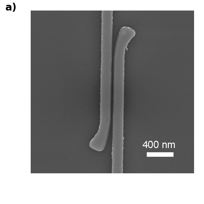
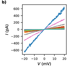
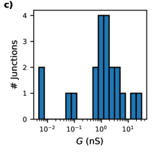
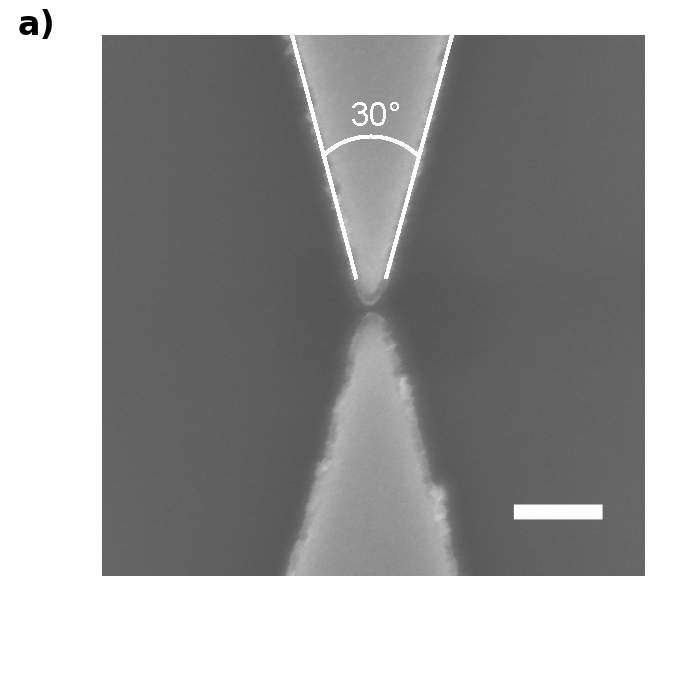
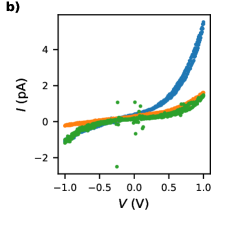
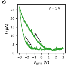
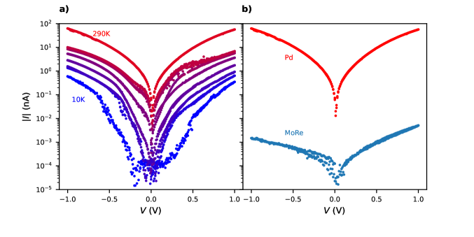
9-AGNR devices with needle-like 10-nm MoRe nanogaps are also characterized at room temperature in vacuum. In Fig. 3 we show a representative SEM image of the needle-like MoRe electrodes. The GNR film was transferred onto 32 pre-fabricated nanogaps. The current is measured versus the applied bias voltage up to 1 V. curves of the conductive devices are shown together in Fig. 3. Three devices are found to have a current above the noise level within this range. The curves are nonlinear with a maximum current of 1 to 5 pA. The electrical characteristics of the two devices shown by the blue and orange curves display an asymmetry in current versus the bias-voltage which is mostly independent of the polarity of the source-drain contacts and can be explained by a capacitive coupling of the source and drain electrodes to the GNRs (see SI, section 3). The current through the junctions was also characterized versus local bottom-gate voltage () at a fixed bias voltage of = 1 V. This is shown in Fig. 3 for the device represented by the green curve in Fig. 3. The sweep directions of the gate voltage are indicated by the arrows. The observed hysteresis (additional results on time dependence in SI, section 4) in the trace and retrace gate-sweeps is similar to what has been reported for 7-AGNR devices at room temperature in air 42, as well as in vacuum for 5-AGNR and 9-AGNR devices for temperatures between 5 and 262 K 43. Furthermore, the current is the largest at negative gate voltages, which is indicative of p-type behavior of the 9-AGNR FETs.
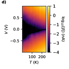
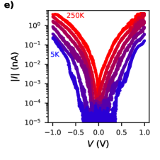
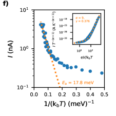
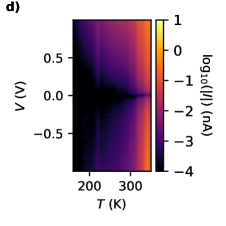
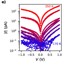
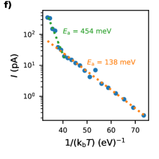
Similar to the measurements on the wide-nanogap geometry, the characteristic of the 10-nm nanogaps is measured versus temperature (measurements of another device in SI, section 1). At a fixed , curves were first measured cooling down from 290 K to 160 K, below which the current gets smaller than the noise floor of 100 fA. To obtain additional information, curves are also measured warming up from 290 K to 350 K. The resulting curves are shown in Fig. 3 as a colormap, with a few individual traces in Fig. 3. As observed in the wide-nanogap MoRe GNR devices, the current decreases by orders of magnitude as the temperature is lowered. In the needle-like MoRe devices, the asymmetry of the current with bias voltage also increases as the temperature is decreased. In contrast to what was observed in the wide-nanogap geometry in Fig. 2, the slope of the log(current)-voltage characteristic is smaller in the 10-nm nanogap devices. The temperature dependence of the current at a bias voltage of 1 V versus inverse temperature is plotted in Fig. 3. Activation energies are once again extracted by fitting the current versus temperature at 1 V using equation 1, which results in meV for K and meV for K. The obtained for the MoRe 9-AGNR devices are an order of magnitude larger in 10-nm nanogap than those found for the wide-nanogap geometry.
Finally, we measured the characteristic of 9-AGNR devices with 10-nm nanogap geometry made of the larger work function noble metal Pd as a function of temperature. Pd is well-known for making low-resistance Ohmic electrical contacts to CNTs, as well as GNRs 5, which makes it an excellent metal to compare with MoRe as a reference. Out of the 32 devices onto which 9-AGNRs were transferred, 2 were found to be electrically conductive. The curves at various temperatures for one device are shown in Fig. 4a (measurements of another device in SI, section 1. Furthermore a nuclear tunneling scaling analysis can be found in the SI, section 5). The characteristic of the selected Pd device is bias symmetric. The slope of the log(I)-V characteristic is small, but larger than that measured for the MoRe 10-nm nanogaps. The devices with Pd contacts show a weaker temperature dependence of the characteristics than those with MoRe contacts (shown in Fig. 3). At K, the current is still orders of magnitude above the noise level, with currents up to pA at V bias voltage. In Fig. 4b the characteristic of the 10-nm Pd nanogap 9-AGNR device is compared with that of the most conductive MoRe nanogap of the same geometry, at room temperature. The conductance of the MoRe devices is four orders of magnitude smaller than the Pd devices at a bias voltage of V.
Discussion
In the characteristics of wide-nanogap MoRe 9-AGNR devices, one thing that stands out is the variation in conductance by 4 orders of magnitude. Some variation is expected due to inherent uncertainty in the transfer method. The GNRs are not globally aligned and may have lost local alignment during the transfer. The numbers of GNRs present in the different devices varies due to the inherent randomness of GNR film growth and positioning on the devices. Improvements can be made with regard to the effect of GNR alignment by growing and transferring globally aligned GNRs on Au (788) surfaces onto devices. In this case the alignment can be also be monitored by polarized Raman spectroscopy44. For 5-AGNR devices, aligned growth on Au (788) has been shown to significantly improve the device yield and conductance23. The variation in device conductance over orders of magnitude however points towards large variation in GNR conductance. This could possibly be explained by oxidation or inhomogeneity of the sputtered MoRe alloy contact, which would results in additional tunnel barriers and spatially varying work functions. Another possible explanation is that the gold etchant introduces a spatially non-uniform doping profile over the devices, resulting in variable band alignment.
Another peculiarity is the kink at 80 K in Fig. 2, which is suggestive of a change in the transport regime. The kink occurs at a voltage of approximately 200 mV, for which . This corresponds to the kink in the nuclear tunneling scaling plot in the inset of Fig. 2. In the context of the nuclear tunneling model, this suggests that the kink may be a transition from a thermally dominated regime to a bias voltage-driven regime.
The fact that the temperature and voltage dependence of the wide-nanogap MoRe 9-AGNR devices can be described using a nuclear tunneling model is surprising, considering the fact that the contact spacing is smaller than the average length of the GNRs. The earlier study by Richter et al. 25 described a possible hopping process from ribbon to ribbon. This suggests that either the dominant transport path is through roughly GNRs or that the hopping process occurs within single GNRs with a length scale between nm and nm. The hopping sites may be local trap states, in which case the sub-sections in the GNR itself act as the charge transport barrier. Such trap states could be present due to a multitude of possible causes, such as overlapping of the GNRs due to rearrangement during substrate transfer, iodine doping after the conventional wet transfer technique used for the wide-nanogaps, as well as adsorbates or charge puddles 45, 46. If the transport through our wide-nanogap MoRe devices is dominated by trap sites, that may also explain the large variability in resistances. A sparse trap density with random placement/barrier widths could result in a large variation in conductance.
For the needle-like devices, the expected device yield, based on random angular alignment only, is . This is significantly larger than the observed yield, which suggests that there is a mechanism that decreases the observed device yield. We identify two possible mechanisms that could reduce device yield. Firstly, the probability of a GNR to bridge the electrodes could be reduced by rearrangements of the GNR film. Clustering/stacking of GNRs, variations in GNR density or the dissolution of GNRs into the PMMA layer and contact defects such as surface oxidation could reduce the device yield (See SI, section 6, for the Raman spectra on MoRe). Secondly, the observed device yield can be lower than the number of devices containing GNRs. We suspect the latter could be the case as the measured devices are close to the lower limit of measurable conductances in our setup ( pS)
The characteristic of the needle-like MoRe nanogap 9-AGNR devices display a significantly smaller slope of the log(current)-voltage characteristic. The most likely explanation for this is the gate voltage of V, applied to improve the signal-to-noise ratio. In SI section 7, we show that the normalized curves get increasingly more linear as the gate voltage goes from to V. Another possible reason for the difference in linearity is that the dominant transport mechanism for these junctions is different, as transport can occur over a source-drain distance of only nm. This distance is smaller than the segment length found for the wide-nanogap MoRe devices.
From the temperature dependence of the characteristic at V, the extracted can be related to the band alignment of the contact metal with the valence band of the GNR at p-type contacts. A lower implies better band alignment and a smaller Schottky barrier. The extracted for the MoRe-based 9-AGNR devices are an order of magnitude larger in 10-nm nanogaps compared with that in wide nanogaps. Note that for these devices, the used geometry, gate dielectric, and transfer methods are different.
We believe it is unlikely that the geometry itself plays a significant role in the band alignment on the metal surface. It is possible that the high- HfO2 and Pt local gate influence the band alignment if the GNR-metal contact is close to the oxide interface. The effective vacuum () distance between the Pt and the GNR is about - nm. For CNTs embedded in Pt, an expected p-doping of eV was found by ab-initio calculations using a density functional theory + non-equilibrium Green’s function simulation 47. Assuming a similar doping effect for GNRs over a larger distance than the van der Waals gap of nm 48, the expected doping is of the order of meV, which is in magnitude comparable to the observed mismatch in activation energies. This would however result in a better valence band alignment of the GNRs in the 10-nm nanogap devices and lower activation energies, which is the opposite of what was observed. Thus this explanation based on geometry can not explain our observations.
The transfer method may also influence the MoRe/GNR contact by means of doping. In particular, the gold etchant step, which produces iodine complexes, is known to result in p-type doping of graphene 49. Nanoparticle gold residues can also potentially introduce n-doping50. In the PMMA-membrane-based transfer technique, no contact of the gold etchant with the electrode was made and a considerably longer rinse and soak time, 8 to 24 hours versus 5 minutes, was used after the gold etchant step. This could have resulted in a lower doping level of the GNRs when compared to the conventional polymer-free wet transfer (used for wide nanogaps) and consequently worsen the band-alignment with MoRe. Besides, the GNRs are covered by PMMA after the membrane-transfer, which may by itself influence the doping of the GNRs.
To get a better understanding of the quality of the MoRe-GNR contact, a comparison with other contact metals is desirable. Activation energies are not as widely reported in the literature as room temperature resistances 5, 17, 25, 19, 51. Thus, to compare with other devices, we use the room-temperature resistance per unit of contact width as a benchmark, similar to what is done for 2D materials 52. The conductance of needle-like MoRe devices with 10-nm nanogaps is around 1 pS for a contact width of around 20 nm, while for the 2 m wide MoRe contacts an average conductance of approximately 1 nS was found. This translates to a conductance per unit width of and , respectively.
For comparison, our Pd 10-nm nanogaps exhibit a current of 1 nA at 0.1 V, resulting in a conductance of 10 nS over the contact width of around 20 nm, which translates to . With the sample contact geometry and PMMA-assisted GNR transfer technique, the reference Pd nanogaps show significantly lower resistances than the MoRe ones. Together with the reduced temperature dependence, this suggests that the band alignment of the Pd work function with the 9-AGNR valence band is better. This could have been partially expected based on the fact that the work function of Pd ( eV 53) is larger than the work function of MoRe ( - eV 54, 55) (See SI, section 8, for a schematic of the estimated band alignment). Another possible explanation for a larger contact resistance for MoRe contacts is the presence of a thin insulating layer on the MoRe surface. Although MoRe alloys are known to have noble-metal-like properties, surface oxidation is yet possible 56.
Recently, 9-AGNR devices with Pt wide-nanogap contacts have been studied at room temperature 51. It was found that the devices made by PMMA-based GNR transfer have a larger contact resistance than those made by polymer-free GNR transfer. This results suggests that it is well possible that the difference observed between the average conductance of the two types of MoRe devices could similarly in part be an effect of the two different transfer methods. For 1-m wide Pt contacts with 50 nm spacing, the reported average conductance for the devices made with PMMA-based GNR transfer and with polymer-free GNR transfer is and , respectively.
As a final remark, we note that our MoRe contacts to GNRs show larger contact resistances than expected based on studies on MoRe-CNT junctions, in which resistances smaller than M per nanotube were obtained 34, 35. A possible explanation for this difference could be that in studies with CNTs, nanotubes were grown or annealed at temperatures higher than ∘C on top of the MoRe contacts, resulting in molybdenum-carbon end bonds. Since no such annealing step was performed for our GNR devices, we do not expect chemical bonds between the MoRe and the GNRs. Another possible explanation for the high resistance of our 9-AGNR devices made with MoRe is that the work function of MoRe is too low to achieve a good p-type contact, while it is closer to the work function of graphene ( - eV 57, 58). This explanation is supported by the ambipolar response in the gate dependence of our MoRe devices, which we show in Fig. S5 and Fig. S6 in the SI. This suggests that MoRe could still be a good contact metal for GNRs with smaller band-gaps, such as 17-AGNRs 59, while larger band-gap GNRs are better contacted by high work function metals such as Pd and Pt.
For 9-AGNR devices with superconducting contacts, further advances could be made by doping the 9-AGNRs or modifying the metal/9-AGNR interface by thermal annealing. To reduce contact resistances with MoRe, GNRs with smaller band gaps could also be considered. In addition, the effective work function of superconductors such as MoRe, Nb or NbTiN could be increased, and thus brought into better alignment with valence band of GNRs, by applying a thin coating of Pd or Pt to their surface, e.g. in a hybrid Pd/MoRe heterostructure.
Conclusion
9-atom-wide armchair GNRs were transferred onto pre-fabricated wide and 10-nm MoRe nanogap contacts, as well as onto Pd electrodes with 10-nm nanogaps. To facilitate GNR transfer onto chemically fragile electrodes, we introduce a PMMA-membrane assisted transfer technique for the 10-nm MoRe nanogap contacts, which allows for controlled handling and micron-precise placement of the GNR film without exposing the electrodes to any liquid. We characterized the conductance of the devices as a function of bias voltage and temperature. In the devices, the electrical resistance increases with decreasing temperature. The -dependence of the characteristics of the wide MoRe nanogap devices can be described by a nuclear tunneling model with a dimensionless dissipation coefficient and hopping sites. This is despite the average GNR size of 45 nm exceeding the electrode separation of 30 nm. In comparison, the needle-like MoRe 10-nm nanogaps show a stronger -dependence of conductance with an order of magnitude larger activation energies. The 10-nm MoRe nanogaps also show field-effect response to the local gate, indicating a p-type metal-semiconductor contact. Pd nanogaps show four orders of magnitude higher conductance for the same bias voltage at room temperature with smaller activation energies than MoRe nanogaps. That suggests the possibility of using Pd/MoRe bilayer thin film electrodes for obtaining low-resistance electrical contacts to GNRs for the realization of superconducting metallic electrodes with a nano-scale geometry down to the limit of addressing a single GNR.
Methods
GNR synthesis. 9-AGNRs were synthesized from 3’,6’-diiodo-1,1’:2’,1”-terphenyl (DITP) 37. Au(111)/mica (Phasis, Switzerland) surface was cleaned in ultrahigh vacuum by two sputtering/annealing cycles: 1 kV Ar+ for 10 min followed by annealing at 470 ∘C for 10 min. In the next step, the precursor monomer DITP was sublimed onto the Au(111) surface from a quartz crucible heated to 70 ∘C, with the substrate held at room temperature. After deposition of approximately one monolayer DITP, the substrate was heated (0.5 K/s) to 200 ∘C for 10 minutes to activate the polymerization reaction, followed by annealing at 400 ∘C (0.5 K/s) for 10 minutes to form the GNRs via cyclodehydrogenation.
Fabrication of contact electrodes. For all devices, 285 nm SiO2 on highly-doped p-type Si substrates were cleaned in red fuming nitric acid for at least 5 min. prior to processing. This was followed by a 5 min. O2 plasma step at a flow of 600 sccm and a power of 600 W in a barrel etcher prior to spin coating of e-beam resist. For the wide-nanogap MoRe devices, the e-beam resist AR-P 6200.04 was spin-coated onto the substrates at 4000 RPM and baked at 185 ∘C for 3 min., resulting in an 80 nm thick film.
The wide-nanogap geometry was written by an e-beam pattern generator at 100 kV with a m aperture at a beam current of pA. The exposed pattern was developed in pentyl acetate for 1 min., followed by a 5 s descum in xylene 60 and a 30 s rinse in isopropyl alcohol, followed by N2 blow drying. A 62:38 MoRe alloy was RF sputtered at an argon pressure of 15 bar and a power of 100 for 1 min to yield an approximately 20 nm thick layer. Finally, metal lift-off was performed by soaking the samples in the remover AR 600-71 at 70 ∘C, followed by a rinse in isopropyl alcohol and N2 blow drying.
For the e-beam exposure of the needle-like nanogap pattern an overdose-undersize (ODUS) procedure with a shape-proximity error correction algorithm was performed 61, 62. The development was done in pentyl acetate developer that was cooled to ∘C in a freezer, as this has been shown to improve contrast for resists that are exposed by polymer chain scission 63. Upon overdosing to 1000 - 2000 the pattern, 6 - 10 nm electrode separations result. The contact pads were kept further than 100 m from the nanogaps to minimize exposure by back-scattered electrons and exposed at 600 . MoRe was sputtered in the same manner as described for the wide-nanogap contacts. 5 nm Ti and 12 nm Pd were deposited by e-beam evaporation at a rate of nm/s and nm/s respectively.
The MoRe needle-like electrodes were made on top of an evaporated 5 nm Ti + 10 nm Pt local bottom gate covered by a 12 nm thick HfO2 high- dielectric layer made by atomic layer deposition at 110 ∘C.
PMMA-membrane fabrication
The procedure for suspension and transfer of the PMMA membranes, based on the technique by Kaverzin et al.64, is as follows; We start with spin coating a thick layer of a water-soluble polymer, in this case, Elektra 92, onto silicon oxide wafers. Next, a 1000 m thick layer of PMMA 950K was spin-coated onto the Elektra 92 layer in two steps, baked at 180 ∘C for 1 min after each step. A rectangular hole was cut in a piece of scotch tape, which was subsequently pressed against the PMMA membrane on silicon. The scotch tape was suspended over a beaker filled with DI water with the silicon piece submerged to dissolve the Elektra 92. After the silicon piece detached from the PMMA membrane, the membrane was rinsed and left to dry in ambient conditions. The dry PMMA membrane was next stretched over a piece of Polydimethylsiloxane (PDMS), placed on a glass slide.
1 Acknowledgments
This work was supported by the Netherlands Organisation for Scientific Research (NWO/OCW), as part of the Frontiers of Nanoscience program. T.S.G. also received funding from the European Union Horizon 2020 research and innovation program under grant agreement no. 863098 (SPRING). G.B.B., P.R. and R.F acknowledge the European Union Horizon 2020 research and innovation program under grant agreement no. 881603 (GrapheneFlagship Core 3) and the Office of Naval Research BRC Program under the grant N00014-18-1-2708. G.B.B., P.R. and R.F. also greatly appreciate the financial support from the Werner Siemens Foundation (CarboQuant). This research was funded, in whole or in part by the Swiss National Science Foundation under Grant No. 200020_182015. For the purpose of Open Access, the author has applied a CC BY public copyright license to any Author Accepted Manuscript version arising from this submission
Supporting information
See the supporting information for an analysis of additional devices, additional electrical characterization, Raman spectroscopy characterization of the transferred 9-AGNR films, band diagrams and optical microscopy images of the MoRe 9-AGNR devices.
Author Declarations
Conflict of Interest
The authors have no conflicts to disclose.
Data Availability Statement
The data that support the findings of this study are available from the corresponding author upon request.
References
- Nakada et al. 1996 Nakada, K.; Fujita, M.; Dresselhaus, G.; Dresselhaus, M. S. Edge state in graphene ribbons: Nanometer size effect and edge shape dependence. Phys. Rev. B 1996, 54, 17954–17961
- Son et al. 2006 Son, Y.-W.; Cohen, M. L.; Louie, S. G. Energy Gaps in Graphene Nanoribbons. Phys. Rev. Lett. 2006, 97, 216803
- Yang et al. 2007 Yang, L.; Park, C.-H.; Son, Y.-W.; Cohen, M. L.; Louie, S. G. Quasiparticle Energies and Band Gaps in Graphene Nanoribbons. Phys. Rev. Lett. 2007, 99, 186801
- Schwierz 2010 Schwierz, F. Graphene transistors. Nat. Nanotechnol. 2010, 5, 487–496
- Llinas et al. 2017 Llinas, J. P.; Fairbrother, A.; Borin Barin, G.; Shi, W.; Lee, K.; Wu, S.; Yong Choi, B.; Braganza, R.; Lear, J.; Kau, N.; Choi, W.; Chen, C.; Pedramrazi, Z.; Dumslaff, T.; Narita, A.; Feng, X.; Müllen, K.; Fischer, F.; Zettl, A.; Ruffieux, P.; Yablonovitch, E.; Crommie, M.; Fasel, R.; Bokor, J. Short-channel field-effect transistors with 9-atom and 13-atom wide graphene nanoribbons. Nat. Commun. 2017, 8, 633
- Miao et al. 2021 Miao, W.; Wang, L.; Mu, X.; Wang, J. The magical photoelectric and optoelectronic properties of graphene nanoribbons and their applications. J. Mater. Chem. C 2021, 9, 13600–13616
- Son et al. 2006 Son, Y.-W.; Cohen, M. L.; Louie, S. G. Half-metallic graphene nanoribbons. Nature 2006, 444, 347–349
- Tao et al. 2011 Tao, C.; Jiao, L.; Yazyev, O. V.; Chen, Y.-C.; Feng, J.; Zhang, X.; Capaz, R. B.; Tour, J. M.; Zettl, A.; Louie, S. G.; Dai, H.; Crommie, M. F. Spatially resolving edge states of chiral graphene nanoribbons. Nat. Phys. 2011, 7, 616–620
- Martin and Blanter 2009 Martin, I.; Blanter, Y. M. Transport in disordered graphene nanoribbons. Phys. Rev. B 2009, 79, 235132
- Brede et al. 2023 Brede, J.; Merino-Díez, N.; Berdonces, A.; Sanz, S.; Domínguez-Celorrio, A.; Lobo-Checa, J.; Vilas-Varela, M.; Peña, D.; Frederiksen, T.; Pascual, J. I.; de Oteyza, D. G.; Serrate, D. Detecting the spin-polarization of edge states in graphene nanoribbons. 2023; https://arxiv.org/abs/2301.11370
- Cai et al. 2010 Cai, J.; Ruffieux, P.; Jaafar, R.; Bieri, M.; Braun, T.; Blankenburg, S.; Muoth, M.; Seitsonen, A. P.; Saleh, M.; Feng, X.; Müllen, K.; Fasel, R. Atomically precise bottom-up fabrication of graphene nanoribbons. Nature 2010, 466, 470–473
- Ruffieux et al. 2016 Ruffieux, P.; Wang, S.; Yang, B.; Sánchez-Sánchez, C.; Liu, J.; Dienel, T.; Talirz, L.; Shinde, P.; Pignedoli, C. A.; Passerone, D.; Dumslaff, T.; Feng, X.; Müllen, K.; Fasel, R. On-surface synthesis of graphene nanoribbons with zigzag edge topology. Nature 2016, 531, 489–492
- Gröning et al. 2018 Gröning, O.; Wang, S.; Yao, X.; Pignedoli, C. A.; Borin Barin, G.; Daniels, C.; Cupo, A.; Meunier, V.; Feng, X.; Narita, A.; Müllen, K.; Ruffieux, P.; Fasel, R. Engineering of robust topological quantum phases in graphene nanoribbons. Nature 2018, 560, 209–213
- Rizzo et al. 2018 Rizzo, D. J.; Veber, G.; Cao, T.; Bronner, C.; Chen, T.; Zhao, F.; Rodriguez, H.; Louie, S. G.; Crommie, M. F.; Fischer, F. R. Topological band engineering of graphene nanoribbons. Nature 2018, 560, 204–208
- Rizzo et al. 2020 Rizzo, D. J.; Veber, G.; Jiang, J.; McCurdy, R.; Cao, T.; Bronner, C.; Chen, T.; Louie, S. G.; Fischer, F. R.; Crommie, M. F. Inducing metallicity in graphene nanoribbons via zero-mode superlattices. Science 2020, 369, 1597–1603
- Bronner et al. 2013 Bronner, C.; Stremlau, S.; Gille, M.; Brauße, F.; Haase, A.; Hecht, S.; Tegeder, P. Aligning the Band Gap of Graphene Nanoribbons by Monomer Doping. Angew. Chem. Int. Ed. Engl. 2013, 52, 4422–4425
- Martini et al. 2019 Martini, L.; Chen, Z.; Mishra, N.; Barin, G. B.; Fantuzzi, P.; Ruffieux, P.; Fasel, R.; Feng, X.; Narita, A.; Coletti, C.; Müllen, K.; Candini, A. Structure-dependent electrical properties of graphene nanoribbon devices with graphene electrodes. Carbon 2019, 146, 36–43
- El Abbassi et al. 2020 El Abbassi, M.; Perrin, M. L.; Barin, G. B.; Sangtarash, S.; Overbeck, J.; Braun, O.; Lambert, C. J.; Sun, Q.; Prechtl, T.; Narita, A.; Müllen, K.; Ruffieux, P.; Sadeghi, H.; Fasel, R.; Calame, M. Controlled Quantum Dot Formation in Atomically Engineered Graphene Nanoribbon Field-Effect Transistors. ACS Nano 2020, 14, 5754–5762, PMID: 32223259
- Braun et al. 2021 Braun, O.; Overbeck, J.; El Abbassi, M.; Käser, S.; Furrer, R.; Olziersky, A.; Flasby, A.; Borin Barin, G.; Sun, Q.; Darawish, R.; Müllen, K.; Ruffieux, P.; Fasel, R.; Shorubalko, I.; Perrin, M. L.; Calame, M. Optimized graphene electrodes for contacting graphene nanoribbons. Carbon 2021, 184, 331–339
- Zhang et al. 2023 Zhang, J.; Braun, O.; Barin, G. B.; Sangtarash, S.; Overbeck, J.; Darawish, R.; Stiefel, M.; Furrer, R.; Olziersky, A.; Müllen, K.; Shorubalko, I.; Daaoub, A. H. S.; Ruffieux, P.; Fasel, R.; Sadeghi, H.; Perrin, M. L.; Calame, M. Tunable Quantum Dots from Atomically Precise Graphene Nanoribbons Using a Multi-Gate Architecture. Adv. Electron. Mater. 2023, 9, 2201204
- Zhang et al. 2022 Zhang, J.; Qian, L.; Barin, G. B.; Daaoub, A. H. S.; Chen, P.; Müllen, K.; Sangtarash, S.; Ruffieux, P.; Fasel, R.; Sadeghi, H.; Zhang, J.; Calame, M.; Perrin, M. L. Ultimately-scaled electrodes for contacting individual atomically-precise graphene nanoribbons. 2022; https://arxiv.org/abs/2209.04353
- Mutlu et al. 2021 Mutlu, Z.; Lin, Y.; Barin, G. B.; Zhang, Z.; Pitner, G.; Wang, S.; Darawish, R.; Giovannantonio, M. D.; Wang, H.; Cai, J.; Passlack, M.; Diaz, C. H.; Narita, A.; Müllen, K.; Fischer, F. R.; Bandaru, P.; Kummel, A. C.; Ruffieux, P.; Fasel, R.; Bokor, J. Short-Channel Double-Gate FETs with Atomically Precise Graphene Nanoribbons. 2021 IEEE International Electron Devices Meeting (IEDM). 2021; pp 37.4.1–37.4.4
- Borin Barin et al. 2022 Borin Barin, G.; Sun, Q.; Di Giovannantonio, M.; Du, C.-Z.; Wang, X.-Y.; Llinas, J. P.; Mutlu, Z.; Lin, Y.; Wilhelm, J.; Overbeck, J.; Daniels, C.; Lamparski, M.; Sahabudeen, H.; Perrin, M. L.; Urgel, J. I.; Mishra, S.; Kinikar, A.; Widmer, R.; Stolz, S.; Bommert, M.; Pignedoli, C.; Feng, X.; Calame, M.; Müllen, K.; Narita, A.; Meunier, V.; Bokor, J.; Fasel, R.; Ruffieux, P. Growth Optimization and Device Integration of Narrow-Bandgap Graphene Nanoribbons. Small 2022, 18, 2202301
- Lin et al. 2023 Lin, Y. C.; Mutlu, Z.; Borin Barin, G.; Hong, Y.; Llinas, J. P.; Narita, A.; Singh, H.; Müllen, K.; Ruffieux, P.; Fasel, R.; Bokor, J. Scaling and statistics of bottom-up synthesized armchair graphene nanoribbon transistors. Carbon 2023, 205, 519–526
- Richter et al. 2020 Richter, N.; Chen, Z.; Tries, A.; Prechtl, T.; Narita, A.; Müllen, K.; Asadi, K.; Bonn, M.; Kläui, M. Charge transport mechanism in networks of armchair graphene nanoribbons. Sci. Rep. 2020, 10, 1988
- Chen et al. 2005 Chen, Z.; Appenzeller, J.; Knoch, J.; Lin, Y.-m.; Avouris, P. The Role of Metal-Nanotube Contact in the Performance of Carbon Nanotube Field-Effect Transistors. Nano. Lett. 2005, 5, 1497–1502
- Svensson and Campbell 2011 Svensson, J.; Campbell, E. E. B. Schottky barriers in carbon nanotube-metal contacts. J. Appl. Phys. 2011, 110, 111101
- Matsuda et al. 2010 Matsuda, Y.; Tahir-Kheli, J.; Goddard, W. A. I. Definitive Band Gaps for Single-Wall Carbon Nanotubes. J. Phys. Chem. Lett. 2010, 1, 2946–2950
- Zhang et al. 2000 Zhang, Y.; Franklin, N. W.; Chen, R. J.; Dai, H. Metal coating on suspended carbon nanotubes and its implication to metal–tube interaction. Chem. Phys. Lett. 2000, 331, 35–41
- Sarkar et al. 2014 Sarkar, S.; Moser, M. L.; Tian, X.; Zhang, X.; Al-Hadeethi, Y. F.; Haddon, R. C. Metals on Graphene and Carbon Nanotube Surfaces: From Mobile Atoms to Atomtronics to Bulk Metals to Clusters and Catalysts. Chem. Mater. 2014, 26, 184–195
- Javey et al. 2003 Javey, A.; Guo, J.; Wang, Q.; Lundstrom, M.; Dai, H. Ballistic carbon nanotube field-effect transistors. Nature 2003, 424, 654–657
- Mann et al. 2003 Mann, D.; Javey, A.; Kong, J.; Wang, Q.; Dai, H. Ballistic Transport in Metallic Nanotubes with Reliable Pd Ohmic Contacts. Nano. Lett. 2003, 3, 1541–1544
- Cao et al. 2015 Cao, Q.; Han, S. J.; Tersoff, J.; Zhu, Y.; Zhang, Z.; Tulevski, G. S.; Tang, J.; Haensch, W. End-bonded contacts for carbon nanotube transistors with low, size-independent resistance. Science 2015, 350, 68–72
- Schneider et al. 2012 Schneider, B. H.; Etaki, S.; van der Zant, H. S. J.; Steele, G. A. Coupling carbon nanotube mechanics to a superconducting circuit. Sci. Rep. 2012, 2, 599
- Kaikkonen et al. 2020 Kaikkonen, J.-P.; Sebastian, A. T.; Laiho, P.; Wei, N.; Will, M.; Liao, Y.; Kauppinen, E. I.; Hakonen, P. J. Suspended superconducting weak links from aerosol-synthesized single-walled carbon nanotubes. Nano Res. 2020, 13, 3433–3438
- Meissner 1960 Meissner, H. Superconductivity of Contacts with Interposed Barriers. Phys. Rev. 1960, 117, 672–680
- Di Giovannantonio et al. 2018 Di Giovannantonio, M.; Deniz, O.; Urgel, J. I.; Widmer, R.; Dienel, T.; Stolz, S.; Sánchez-Sánchez, C.; Muntwiler, M.; Dumslaff, T.; Berger, R.; Narita, A.; Feng, X.; Müllen, K.; Ruffieux, P.; Fasel, R. On-Surface Growth Dynamics of Graphene Nanoribbons: The Role of Halogen Functionalization. ACS Nano 2018, 12, 74–81, PMID: 29200262
- Borin Barin et al. 2019 Borin Barin, G.; Fairbrother, A.; Rotach, L.; Bayle, M.; Paillet, M.; Liang, L.; Meunier, V.; Hauert, R.; Dumslaff, T.; Narita, A.; Müllen, K.; Sahabudeen, H.; Berger, R.; Feng, X.; Fasel, R.; Ruffieux, P. Surface-Synthesized Graphene Nanoribbons for Room Temperature Switching Devices: Substrate Transfer and ex Situ Characterization. ACS Appl. Nano. Mater. 2019, 2, 2184–2192
- Fisher and Dorsey 1985 Fisher, M. P. A.; Dorsey, A. T. Dissipative Quantum Tunneling in a Biased Double-Well System at Finite Temperatures. Phys. Rev. Lett. 1985, 54, 1609–1612
- Grabert and Weiss 1985 Grabert, H.; Weiss, U. Quantum Tunneling Rates for Asymmetric Double-Well Systems with Ohmic Dissipation. Phys. Rev. Lett. 1985, 54, 1605–1608
- Bockrath et al. 1999 Bockrath, M.; Cobden, D. H.; Lu, J.; Rinzler, A. G.; Smalley, R. E.; Balents, L.; McEuen, P. L. Luttinger-liquid behaviour in carbon nanotubes. Nature 1999, 397, 598–601
- Bennett et al. 2013 Bennett, P. B.; Pedramrazi, Z.; Madani, A.; Chen, Y.-C.; de Oteyza, D. G.; Chen, C.; Fischer, F. R.; Crommie, M. F.; Bokor, J. Bottom-up graphene nanoribbon field-effect transistors. Appl. Phys. Lett. 2013, 103, 253114
- Tries et al. 2020 Tries, A.; Richter, N.; Chen, Z.; Narita, A.; Müllen, K.; Wang, H. I.; Bonn, M.; Kläui, M. Hysteresis in graphene nanoribbon field-effect devices. Phys. Chem. Chem. Phys. 2020, 22, 5667–5672
- Overbeck et al. 2019 Overbeck, J.; Borin Barin, G.; Daniels, C.; Perrin, M. L.; Liang, L.; Braun, O.; Darawish, R.; Burkhardt, B.; Dumslaff, T.; Wang, X.-Y.; Narita, A.; Müllen, K.; Meunier, V.; Fasel, R.; Calame, M.; Ruffieux, P. Optimized Substrates and Measurement Approaches for Raman Spectroscopy of Graphene Nanoribbons. Phys. Status Solidi B 2019, 256, 1900343
- Zhang et al. 2009 Zhang, Y.; Brar, V. W.; Girit, C.; Zettl, A.; Crommie, M. F. Origin of spatial charge inhomogeneity in graphene. Nat. Phys. 2009, 5, 722–726
- Mayamei et al. 2020 Mayamei, Y.; Shin, J. C.; Watanabe, K.; Taniguchi, T.; Bae, M.-H. Landscape of Charge Puddles in Graphene Nanoribbons on Hexagonal Boron Nitride. Phys. Status Solidi B 2020, 257, 2000317
- Fediai et al. 2016 Fediai, A.; Ryndyk, D. A.; Seifert, G.; Mothes, S.; Claus, M.; Schröter, M.; Cuniberti, G. Towards an optimal contact metal for CNTFETs. Nanoscale 2016, 8, 10240–10251
- Sutter et al. 2009 Sutter, P.; Sadowski, J. T.; Sutter, E. Graphene on Pt(111): Growth and substrate interaction. Phys. Rev. B 2009, 80, 245411
- Yao et al. 2019 Yao, Y.; ang Peng, S.; nan Huang, X.; yong Zhang, D.; yuan Shi, J.; Jin, Z. A uniform stable P-type graphene doping method with a gold etching process. Nanotechnology 2019, 30, 405205
- Wu et al. 2012 Wu, Y.; Jiang, W.; Ren, Y.; Cai, W.; Lee, W. H.; Li, H.; Piner, R. D.; Pope, C. W.; Hao, Y.; Ji, H.; Kang, J.; Ruoff, R. S. Tuning the Doping Type and Level of Graphene with Different Gold Configurations. Small 2012, 8, 3129–3136
- Hsu et al. 2023 Hsu, C.; Rohde, M.; Borin Barin, G.; Gandus, G.; Passerone, D.; Luisier, M.; Ruffieux, P.; Fasel, R.; van der Zant, H. S. J.; Abbassi, M. E. Platinum contacts for 9-atom-wide armchair graphene nanoribbons. Appl. Phys. Lett. 2023, 122, 173104
- Allain et al. 2015 Allain, A.; Kang, J.; Banerjee, K.; Kis, A. Electrical contacts to two-dimensional semiconductors. Nat. Mater. 2015, 14, 1195–1205
- Michaelson 1977 Michaelson, H. B. The work function of the elements and its periodicity. J. Appl. Phys. 1977, 48, 4729–4733
- Berge et al. 1974 Berge, S.; Gartland, P.; Slagsvold, B. Photoelectric work function of a molybdenum single crystal for the (100), (110), (111), (112), (114), and (332) faces. Surf. Sci. 1974, 43, 275–292
- Liang et al. 2006 Liang, Y.; Curless, J.; Tracy, C. J.; Gilmer, D. C.; Schaeffer, J. K.; Triyoso, D. H.; Tobin, P. J. Interface dipole and effective work function of Re in Re/HfO2/SiOx/n-Si gate stack. Appl. Phys. Lett. 2006, 88, 072907
- Hoekje et al. 1993 Hoekje, S.; Outlaw, R.; Sankaran, S. Surface compositional variations of Mo-47Re alloy as a function of temperature. NASA Tech. Pap. 3402 1993,
- Song et al. 2012 Song, S. M.; Park, J. K.; Sul, O. J.; Cho, B. J. Determination of Work Function of Graphene under a Metal Electrode and Its Role in Contact Resistance. Nano. Lett. 2012, 12, 3887–3892
- Rut’kov et al. 2020 Rut’kov, E.; Afanas’eva, E.; Gall, N. Graphene and graphite work function depending on layer number on Re. Diam. Relat. Mater. 2020, 101, 107576
- Yamaguchi et al. 2020 Yamaguchi, J.; Hayashi, H.; Jippo, H.; Shiotari, A.; Ohtomo, M.; Sakakura, M.; Hieda, N.; Aratani, N.; Ohfuchi, M.; Sugimoto, Y.; Yamada, H.; Sato, S. Small bandgap in atomically precise 17-atom-wide armchair-edged graphene nanoribbons. Commun. Mater. 2020, 1, 36
- Thoms and Macintyre 2014 Thoms, S.; Macintyre, D. S. Investigation of CSAR 62, a new resist for electron beam lithography. J. Vac. Sci. Technol. B 2014, 32, 06FJ01
- Liu et al. 2002 Liu, K.; Avouris, P.; Bucchignano, J.; Martel, R.; Sun, S.; Michl, J. Simple fabrication scheme for sub-10 nm electrode gaps using electron-beam lithography. Appl. Phys. Lett. 2002, 80, 865–867
- Martens et al. 2013 Martens, S.; Butschke, J.; Galler, R.; Krüger, M.; Sailer, H.; Sülzle, M. E-beam GIDC resolution enhancement technology in practical applications. Photomask Technology 2013. 2013; p 88802H
- Ocola and Stein 2006 Ocola, L. E.; Stein, A. Effect of cold development on improvement in electron-beam nanopatterning resolution and line roughness. J. Vac. Sci. Technol. B Nanotechnol. Microelectron. 2006, 24, 3061–3065
- Kaverzin et al. 2022 Kaverzin, A. A.; Ghiasi, T. S.; Dismukes, A. H.; Roy, X.; van Wees, B. J. Spin injection by spin–charge coupling in proximity induced magnetic graphene. 2D Mater. 2022, 9, 045003