∎
Tel.: +380-542-222-794
Fax: +380-542-223-760
11email: igor-musienko@ukr.net
Nanoclusters and nanoscale voids as possible sources of increasing dark current in high-gradient vacuum breakdown
Abstract
The potential barrier model considers an additional current that can lead to the high-gradient breakdowns in accelerating structures is proposed. An oscillatory resonance feature of the field emission current from a double-layer metal system with a nanoscale coating is shown. The double potential barrier was used for calculations of the field emission current density value. The presence of resonant properties of the field emission current density of a double-layer metal system with a nanometric coating is revealed. The field emission current increasing more than 5 times (for the constant value of an electric field strength ) when considering not ideal copper surface with presence of nanoclusters on the surface of or nanoscale voids in the near-surface layer is observed.
Keywords:
field emission current densitypotential barrierthe transmission coefficient of the potential barrierresonant tunnelingfull width at half maximum (FWHM).pacs:
79.70.+q 03.65.Ge1 Introduction
Field emission is a type of emission that is caused by the quantum mechanical tunneling of electrons from the metal surface to a vacuum induced by an electrostatic field r1 . This phenomenon is typical for strong fields with electric field strength V / m. It is one of the main factors, which leads to the dark currents occurring in the accelerating structures and, as a consequence, the loss of electrical insulating properties of the interelectrode gap r2 ; r3 ; r4 . The problem of regulating the magnitude of the field emission current is relevant, in particular, to preventing high-vacuum high-gradient breakdowns. Another important goal is to obtain gradient-stable materials that eliminate the possibility of electric discharge in the components of modern accelerators. The amplification of the field emission current is also important, particularly for the operation of field emission sources, tunnel microscopy requirements, electron holography, vacuum nanoelectronics r5 ; r6 ; r7 ; r8 ; r9 .
Modeling of experimental operating conditions of the compact linear electron-positron collider in the CLIC (Compact Linear Collider) project is carried out at CERN (European Organization for Nuclear Research). It was showed when applied a high-frequency electromagnetic field to the metal surfaces of accelerating structures, which provides an acceleration rate of the order of 100 MV / m, the high-gradient high-vacuum breakdowns occurs r2 ; r3 ; r4 . Since the breakdowns leads to a significant loss of energy and to the damaging surface of facilities components, reducing the probability of its occurrence in the CLIC accelerating structures is a necessary condition for the high-quality functioning of the future collider.
Therefore, various methods of increasing stability of the accelerator modules surface to high-gradient high-vacuum breakdown are being studied. Among the possible methods to prevent high-gradient breakdowns are metal surface modification by implanting argon, nitrogen, zirconium ions into the near-surface copper layer (which is the base material of CLIC accelerating structure disks) and an ion-plasma treatment of the substrate surface by a metal layer with a greater work function r10 .
The effect of changing the electrode surface characteristics on the field emission current density was experimentally investigated in r10 and theoretically in r11 ; r12 . In the article r10 , it was experimentally confirmed that the condition of the electrode surface significantly affects the breakdown voltage. Plasma and ion-beam modification of the copper surface leads to an increase in the high-vacuum breakdown voltage from 5 to 35 % and decrease the dark current in the interelectrode gap. The result with the greatest suppression of the high-vacuum breakdown in the experiments was obtained for copper with the TiN coating and additional irradiation of the surface with the argon ions energy is equal to 300 keV.
In articles r13 ; r14 an effect of a magnetic field on the field emission current was interpreted. The breakdown voltage decrease due to an increase of ionization by the electron impact was predicted. In r15 the possibility of considering the relativistic correction for the field emission current density of electrons from metal is described theoretically. It was found that in the case of the field electron emission from pulsars the relativistic change in the current value is about 10 % of the Fowler-Nordheim current density. In r16 it was found that the presence of an external magnetic field parallel to the metal surface with a value of 10 T leads to a decrease in the transmission coefficient by 10 %. In paper r17 the flash emission with a duration of 1 - 5 ns, induced by a pulsed electric field V / m applied to a cathode, produced of graphene-like structures, was experimentally detected. In contrast to explosive emission r7 the new type of emission is not associated with the appearance of plasma and destruction of local nano- and microregions of the cathode surface.
The investigation r18 shows an effect of the Coulomb blockade phenomenon on the current density value from nanoscale objects. In r19 the low-voltage field emission of electrons from nanostructured carbon materials is theoretically described due to the presence of resonant surface states, provided that the emitter surface has two carbon phases with different electronic properties. The possibility of increasing the emission current due to the resonant tunnelling of electrons through the double potential barrier by four or more orders of magnitude was predicted.
Investigations of the vacuum breakdown mechanism at the prototypes of the future CLIC accelerator showed that the dark current values cannot be explained only by an electric field enhancement by metal surface irregularities r20 . The field emission measurements on a macroscopic system needs a large – 30, 100 or more – correction factor to get current vs voltage data, corresponding to the current density value from the Fowler-Nordheim equation. However, an amplification factor is not enough for corrections of 30 to 100 and more in the case of measuring the field emission current density from a copper surface in experiments performed in the CERN DC Spark Systems (electrodes in ultra high vacuum with a high voltage external circuit, used to study breakdown). Thus, possible sources of dark current amplification, which leads to high-vacuum breakdowns, are now being searched for.
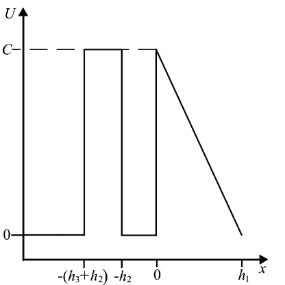
The main idea of this paper is to study the possibility of increasing the field electron emission current in the case of two-layer metal systems by choosing the coating thickness on the substrate. It is similar to a special technique of an anti-reflective coating to reduce losses for the reflection of light r21 ; r22 ; r23 . Figure 1 shows the shape of the double potential barrier, which is considered for calculating the field electron emission current from a two-layer metal system. Similar models of the potential barrier were used to study the properties of quantum wells and resonant tunnelling of the field electron emission through the double barrier r24 ; r25 ; r26 ; r27 ; r28 .
The paper r29 presents an exact analytical theory for field emission from dielectric coated cathode surfaces, by solving the one-dimensional (1D) Schrdinger equation with a double-triangular potential barrier, which is formed by applying dc electric field to the dielectric coated cathode surface. The quantum model in r29 is also compared with a modified Fowler-Nordheim equation for a double-triangular barrier, showing qualitatively good agreement.
The purpose of this study is to perform a numerical calculation of the field electron emission current using the model of the double potential barrier of a rectangular-triangular shape. One of the issues is to explain the analytical relationship between the de Broglie wavelength of the tunnelling electron and the width of the potential well in the case of the double rectangular potential barrier. An important issue is to demonstrate the effect of resonant tunnelling on the field emission current density due to the double potential barrier. This theory is used to find additional sources of increasing the field emission current from the metal surface.
2 Replacement of a single-stage triangular potential barrier with a rectangular one of equal transparency
The double potential barrier for barrier structures in semiconductor layered systems is considered in reference r24 . It is also used to evaluate the value of the field emission current from a double-layer metal-semiconductor system in r29 ; r30 and for estimates the current density from the near-surface copper layer modified by the point vacancies in r12 . The proposed model makes it possible to describe two different objects such as nanoclusters and nanoscale voids.
If there is a nanoscale void in the surface metal layer, in Figure 1 the model represents as the barrier width at the metal-vacuum interface, is the distance from the metal-vacuum interface to the location of the nanoscale void in the surface metal layer, is the nanoscale void diameter. If the nanocluster is located on the metal surface, then the barrier parameters in Figure 1 can be explained as is the barrier width at the metal-vacuum interface, is the nanocluster size, is the dipole layer thickness of the metal to metal contact. Below in this study, the authors will consider the nanoscale voids.
Note that for an authentic model of the potential barrier, it is necessary to take into account the presence of electric field strength in the dipole layer, which occurs upon contact of surfaces of various metals r30 . In the case of two layers of identical metal, the dipole dielectric field is zero.
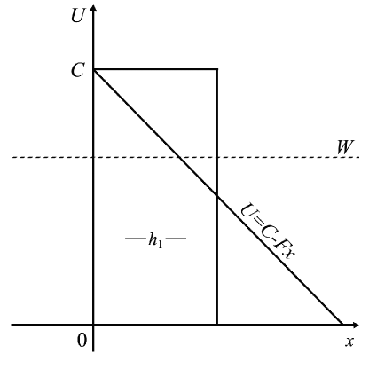
Fowler and Nordheim found the formula for the current emission density based on the determination of the transmission coefficient as a function of the electron energy in the case of the triangular potential barrier at the boundary from the metal to a vacuum. In this investigation, it will be replaced the authentic triangular potential barrier shape shown in Figure 2 by the rectangular one provided that their transmission coefficients are equal. Thus, it is possible to significantly simplify and speed up numerical calculations and avoid mathematical transformations with Hankel functions of the second kind to find the transmission coefficient of the potential barrier. Let us introduce the notation: is the potential energy; the potential energy height ; is the chemical potential; is the work function; ; is the electron charge; is the electric field strength.
The transmission coefficient of a rectangular potential barrier of width r24 ; r31 can be written in the following analytical form in selected convenient notations:
| (1) |
where ; ; ; is the electron mass; .
The expression for the transmission coefficient of the triangular potential barrier, obtained by Fowler and Nordheim r1 , is necessary to find the field electron emission current density at a range of values of the electric field strength V / m and is equal to:
| (2) |
For eV / m it is necessary to use the numerical method of obtaining the complex amplitudes of wave functions and the transmission coefficient of the potential barrier because formula (2) for the above interval is not accurate. From the equality it was obtained the dependence of on the physical quantities and in general form, which is correct for the above-mentioned range of values of the electric field strength :
| (3) |
where is an inverse hyperbolic sine. On condition , equating the right-hand sides of formulas (1) and (2) and not taking into consideration the values of the factors before the exponents of the expressions, an approximate formula was found for the effective :
| (4) |
The approximate expression to formula (3) can be written as:
| (5) |
Figure 3 shows the graphical dependences of on the value of for the parameters of copper eV, . For calculations, it is advisable to take the electron energy near the energy value of the chemical potential , as the most probable current carriers of the field emission from the metal surface are free electrons at the upper energy levels according to Sommerfeld’s theory r1 ; r8 . The graphs of dependences (3) (indicated in Figure 3 by a solid line) and (5) (a line of rings) coincide on the considered interval of values of . Formula (4) (the line is represented by asterisks) approximately describes the analytical dependence .
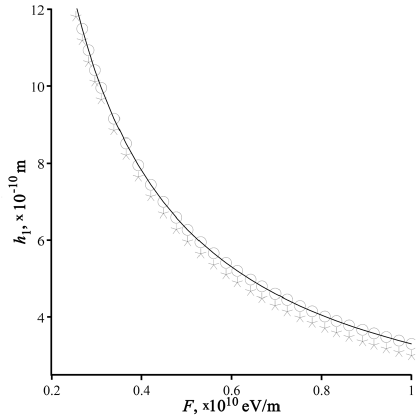
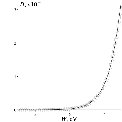
Figure 4 demonstrates the dependences of the width of a rectangular potential barrier on the electron energy for different values of . Thus, if the constant electric field strength increases, then the value of decreases. As a consequence, the width of the rectangular potential barrier narrows, and for values of eV / m, the transmission coefficient increases significantly.
Figure 5 represents the graphic dependences of the transmission coefficient of single-stage potential barriers of triangular and rectangular shapes on the electron energy for the parameters: eV, eV, eV / m. The quantity is determined for an arbitrary energy using expression (5). The curves of dependences are indicated by a solid line in the case of the triangular barrier, and a line of asterisks is constructed as a result of calculations by a numerical method, and a line of squares is used to depict the dependencies for the rectangular barrier, respectively. Therefore, using formula (5), it is possible to quantitatively replace the triangular shape of the barrier with a rectangular one with a width of .
The field emission current density is determined by the expression:
| (6) |
where is the number of electrons emit on a metal surface of unit area per unit time with a kinetic energy normal to the surface. The quantity was evaluated by Nordheim and under the conditions of the problem is found in the form:
| (7) |
The integrand of formula (6) is the differential current:
| (8) |
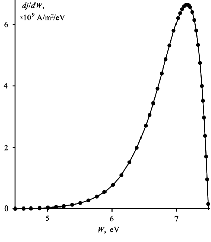
The right-hand side of expression (8) determines the electron energy distribution density. Figure 6 shows the graphic dependences of the differential current on the electron energy at the parameters that were used for Figure 5. In Figure 6 the solid line corresponds to the case of the triangular potential barrier. The line of solid circles is used if the rectangular barrier is considered. As can be seen from Figure 6, the plots of dependences have coincided well for rectangular and triangular shapes of potential barriers.
3 Analysis of the properties of a double potential barrier of rectangular shape
The idea of this model is to emit electrons from the metal surface to a vacuum sequentially through two rectangular potential barriers due to the tunneling effect. In the case of the selected parameters, the probability of an electron with energy passing through a double potential barrier can be higher than for a single-stage barrier, and as a consequence, resonant tunneling of electrons will occur r25 .

Figure 7 shows a simplified for computation potential barrier shape for the metal-metal-vacuum medium with a thickness of the nanoscale metal coating, which is used to find the analytical expression of the transmission coefficient and transfer of the revealed mathematical regularities to the real model of the double potential barrier of a system of two layers of metals. The model is similar to the barrier shape to describe a quantum resonant-tunneling diode r25 . Each of the regions means: V is a metal substrate, IV is a dipole layer of metal-metal contact, III is a coating layer identical to the substrate material, II is a potential barrier at the metal-vacuum interface, I is a vacuum. Region II is a quantitative replacement of triangular barrier by a rectangular one with equal transparency. The coordinates are the boundaries of the specified regions. The parameters , , of the model are the width of regions II, III, IV, respectively. The subscript numbering of the wave vectors coincides with the number of each region. If or , the double potential barrier of a rectangular shape becomes single-stage.
The transmission coefficient of the double potential barrier of rectangular shape in Figure 7 with the same potential energy in regions II and IV is found in analytical form:
| (9) |
where ;
;
;
;
; ;
.
In general, the transmission coefficient of a double barrier with different heights of potential energy regions was found in r24 ; r28 . If or , then formula (9) is simplified to expression (1). Using the condition of maximum manifestation of resonance:
| (10) |
on condition , which simplifies the calculation, formula (9) can be written as:
| (11) |
The condition for the absolute transparency of a double potential barrier of rectangular shape in the case of the expression (10) and at the value is obtained in the form:
| (12) |
where is the de Broglie wavelength of an electron.
At the electron energy eV then m, and using (12), m. It is of importance, that the formula (12), found under condition (10) and the value of . The maximum possible value of is also in the case of violation of the condition (10), but less than one (not absolute transparency). Introduction (10) and is necessary to simplify (9) and find the simple mathematical expression (11) for transparency of the double rectangular barrier.
Applying conditions (10) and m, the transmission coefficient (9) can be represented as a second-order Taylor series near the coordinate :
| (13) |
If m, then formula (13) is simplified to the form:
| (14) |
Figure 8 represents the graphic dependences of the transmission coefficient on the electron energy of the double potential barrier from Figure 7 at eV, m, m. As can be seen from Figure 8, the transmission coefficient maxima of the potential barrier are observed for arbitrary , and the height and width of the graphic dependences peaks are increase with increasing energy . If the value of increases, the width of the peaks decreases.
Figure 9 illustrates the dependences of the differential current on the energy under the conditions eV, eV, m, m in the case of a double potential barrier of rectangular shape (the solid line) and rectangular single-stage barrier (the line is depicted by dots). The parameters , , are selected so that the resonance condition (12) is fulfilled. Thus, the width is multiple to a quarter of the de Broglie wave , which is similar to a special technique of an anti-reflective coating r21 ; r22 ; r23 . An additional coating applied to the metal substrate not only increases transparency but also reduces the energy scattering of field emission electrons in the region of absolute transparency of the double rectangular potential barrier. This conclusion is confirmed by the graphs in Figure 9.
![[Uncaptioned image]](/html/2306.15675/assets/x10.png)
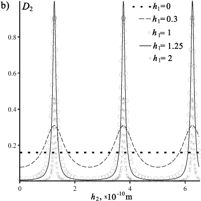
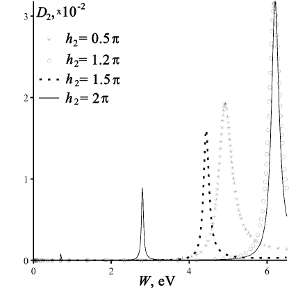
In Figure 10 a), b) it is seen that if eV, , m then the transmission coefficient (11) is the greatest when . By increasing the values of and , the transmission coefficient decreases to zero, but the graphic appearance of the dependencies is retained. From Figure 10 b) it can be concluded that there is the repeatability of maxima and minima of according to formula (12). These peaks were found numerically because it is difficult to experimentally fulfill the condition for the thickness of the coating on the surface of a metal substrate.
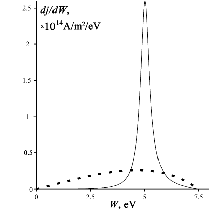
Figure 11 illustrates the graph of the differential current dependence on the electron energy for the barrier model from Figure 7. It is observed the resonance region of the aforementioned quantity near the coordinate of maximum eV. The second peak is the background non- resonance differential current. If there is no potential barrier for the motion of the electron in region IV, which is indicated in Figure 7, the background non-resonance differential current is transformed into a differential field emission current. Figure 11 was obtained under conditions: eV, eV, m. The value of is determined from expression (5) at eV / m.

Therefore, for a theoretical study of the field emission phenomenon from a metal in the presence of nanoscale voids in the surface metal layer, the model of rectangular double potential barrier simplified for calculations is proposed.
4 Simulation of the field emission current through a double barrier in the presence of an external electric field
For verification with analytical results for the barrier in Figure 7, it is calculated by the numerical method the value of the field emission current density from a two-layer metal system in the case of the potential barrier model from Figure 1. First of all, let us compare the dependences of the transmission coefficient and the differential current on for the double barrier, which correspond to Figure 7, and the double barrier in Figure 1.
Figure 12 and Figure 13 were obtained under the conditions: eV, eV, m. The value of is determined for an arbitrary energy from expression (5) at eV / m. The curve depicted by dots corresponds to the dependence for the model in Figure 7. The solid line indicates the dependence graph in the case of the double potential barrier described in Figure 1. Therefore, a quantitative coincidence of dependence graphs is observed at a shift that less than eV in the maxima range of physical quantities. Figure 14 shows two peaks of the dependence graphs of differential current on the electron energy that will be at other values of .
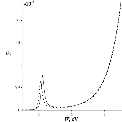
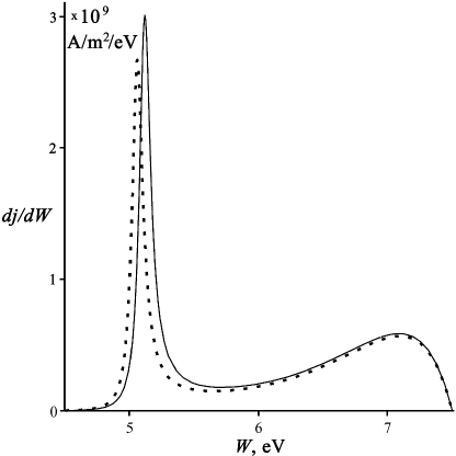
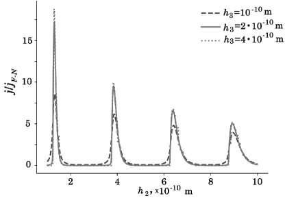
Figure 14 demonstrates the dependence graphs of on obtained by the numerical method at different values of . At the value V / m for the copper characteristics: eV, eV. Then the current from the ideal copper surface is A / m2. In Figure 14 the maxima of the current density are more than 5 times greater than at the above parameters for m.
Properties for the model in Figure 7 will be typical for the double potential barrier from Figure 1. Under the conditions of the selected parameters , , for a system of two metal layers, where the upper layer has a nanoscale thickness, the similar resonant tunneling r25 of electrons will occur and one can observe a reduction of electron energy scattering in the absolute transparency region. From Figure 14 it can be concluded that with increasing the current density oscillations are decreasing. But the important contribution to the dark current in accelerating cavities and, hence, to the field emission current density is given by the oscillations of the current even when the value of the parameter is more than one nanometer. The greatest value of the current density dependence on in Figure 14 is the first maximum at the point , which is similar to a special technique of an anti-reflective coating r21 ; r22 ; r23 .
5 Width investigation of the resonance oscillatory peak of field emission current
Let us evaluate the full width at half maximum () of differential current in the resonance region from Figure 11. One can use the expressions (13) and (14) that correspond to the formula (9). One can find the analytical formula for , taking into account the expression (14) and on condition , in the following form:
| (15) |
The next stage is to approximate the resonant region of the dependence from Figure 11 by a Gaussian function:
| (16) |
Figure 15 shows the dependence graph (16), depicted by a line of triangles at numerically found values: eV, A / m2 / eV, eV, A / m2 / eV. In Figure 15 the solid line describes the resonant region of dependence from Figure 11, obtained numerically. The formula for was found, using (16), and it is written as:
| (17) |
From formula (17) it is found that eV. Thus, the appearance of the resonant maximum region is a characteristic of electrons in a narrow range of energies and selected parameters , , , when the condition (12) is fulfilled.

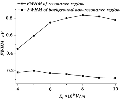
Let us compare the dependence graph of of the two peaks, constructed by a solid line in Figure 13, at different values of the electric field strength . From Figure 16, constructed under conditions eV, eV, m, it is concluded that the value of the differential current dependence on from Figure 13 in the resonant maximum region at different is in a narrow range of energies and is equal to eV. The value of full width at half maximum in the resonant region of the differential current dependence on decreases with increasing . The values for the background non-resonance differential current peak, shown by the line with circles, were found more than 5 times greater in comparison with the results for the resonance maximum region. The values, represented by the line with squares in Figure 16, it is found by the numerical method for the barrier model from Figure 1, are consistent with the analytical result (17) in the case of the potential barrier form in Figure 7.
6 Summary
A potential barrier model has been proposed that takes into account additional mechanisms of high-gradient high-vacuum breakdowns in accelerating structures. It was experimentally confirmed in reference r20 that the field emission current from a real metal surface is greater than the value calculated theoretically. It is assumed that the sources of increased dark current in the accelerating cavities and, consequently, the field emission current from the electrode surface are nanoclusters on the surface and nanoscale voids in the near-surface metal layer.
As a result, it was shown that the field emission current from the metal surface near the nano-objects has an oscillatory resonance feature. The resonance condition (12) determines the size of the nanocluster on the metal surface or the depth of the nanoscale void from the metal surface whose diameter is a multiple of . The current takes on a maximum value when the transmittance is 1 and provided the size of the nanoscale void .
The full width at half maximum () of the resonance region does not depend on the electric field strength, but one depends on the height of the potential barrier and the size . At the parameters eV, eV, m, eV / m, it is found that eV.
It is revealed that at GV / m the field emission current density from copper surface increases more than 5 times in the case of double potential barrier model under the resonance condition (12) compared to .
Acknowledgements.
The publication is based on the research provided by the grant support of the National Academy of Sciences of Ukraine (NASU) for research laboratories/groups of young scientists of the National Academy of Sciences of Ukraine to research priority areas of development of science and technology in 2021 - 2022 under contract No 16 / 01 - 2021 (3). The authors thank to O.P. Novak for helpful discussions on the paper.7 Authors contributions
All the authors were involved in the preparation of the manuscript. All the authors have read and approved the final manuscript.
References
- (1) R.H. Fowler, L. Nordheim, Proc. Roy. Soc. A 119, 173 (1928)
- (2) A. Kyritsakis, M. Veske, K. Eimre, V. Zadin, F. Djurabekova, J. Phys. D: Appl. Phys. 51, 22 (2018)
- (3) Nicholas C. Shipman,in Experimental study of DC vacuum breakdown and application to high-gradient accelerating structures for CLIC (University of Manchester, Manchester, 2014)
- (4) N. Shipman, I. Profatilova, A.T. Perez Fontenla, W. Wuensch, S. Calatroni, CLIC - Note 1078, 1 (2017)
- (5) N. Egorov, E Sheshin, in Field Emission Electronics (Springer Series in Advanced Microelectronics 60, Springer International Publishing AG, 2017)
- (6) G.N. Fursey, in Field emission (Publishing House ”Lan”, St. Petersburg, 2012)
- (7) G.A. Mesyats, in Explosive Electron Emission (Publishing House of Physical and Mathematical Literature, Moscow, 2011)
- (8) G.G. Vladimirov, in Physical Electronics. Emission and Interaction Particles with a Solid (Publishing House ”Lan”, St. Petersburg, 2013)
- (9) M.I. Elinson, G.F. Vasiliev, in Autoelectronic emission (Publishing House of Physical and Mathematical Literature, Moscow, 1958)
- (10) V.A. Baturin, A.Yu. Karpenko, V.E. Storizhko, V.A. Shutko, Probl. At. Sci. Tech. 116, 4 (2018)
- (11) I.I. Musiienko, R.I. Kholodov, Probl. At. Sci. Tech. 121, 3 (2019)
- (12) I.I. Musiienko, R.I. Kholodov, J. Nano- Electron. Phys. 11, 3 (2019)
- (13) S.O. Lebedynskyi, V.I. Miroshnichenko, R.I. Kholodov, V.A. Baturin, Probl. At. Sci. Tech. 98, 4 (2015)
- (14) S. Lebedynskyi, O. Karpenko, R. Kholodov, V. Baturin, Ia. Profatilova, N. Shipman, W. Wuensch, Nucl. Instrum. Methods Phys. Res. A 908, 318 (2018)
- (15) S.O. Lebedynskyi, O.O. Pasko, R.I. Kholodov, J. Nano- Electron. Phys. 11, 2 (2019)
- (16) S. Lebedynskyi, R. Kholodov, Eur. Phys. J. D 73, 190 (2019)
- (17) M.A. Polyakov, G.N. Fursey, J. Commun. Technol. Electron. 63, 239 (2018)
- (18) O.E. Raichev, Phys. Rev. B 73, 195328 (2006)
- (19) Al.A. Zakhidov, A.N. Obraztsov, A.P. Volkov, D.A. Lyashenko, JETP 100, 89 (2005)
- (20) W. Wuensch, in 8th International Workshop on Mechanisms of Vacuum Arcs (MeVArc 2019), Padova, 2019, Field Emission - Modeling and Simulations, 85
- (21) G.S. Landsberg, in Elementary textbook on physics: In three volumes. V. 3. Oscillations and waves. Optics. Atomic and Nuclear Physics (Mir Publishers, Moscow, 1989)
- (22) J. Moghal, J. Kobler, J. Sauer, J. Best, M. Gardener, Andrew A.R. Watt, G. Wakefield, ACS Appl. Mater. Interfaces 4, 854 (2012)
- (23) H.K. Raut, V.A. Ganesh, A.S. Nair, S. Ramakrishna, Energy Environ. Sci. 4, 3779 (2011)
- (24) P. Harrison, in Quantum Wells, Wires, and Dots: Theoretical and Computational Physics of Semiconductor Nanostructures (John Wiley & Sons, Ltd., UK, 2005)
- (25) A.S. Abdalla, M.H. Eisa, R. Alhathlool, O. Aldaghri, Optik 170, 314 (2018)
- (26) Jihad M. Mohaidat, Kai Shum, R.R. Alfano, Phys. Rev. B, Condensed matter 48, 8809 (1993)
- (27) Z. Xiao, D. Shi-sen, Z. Chun-Xi, arXiv preprint arXiv: 1210.0970v2, (2012)
- (28) H.H. Hosack, J. Appl. Phys. 36, 1281 (1965)
- (29) Y. Zhou, P. Zhang, Phys. Rev. Research 2, 043439 (2020)
- (30) N.V. Egorov, L.I. Antonova, A.Yu. Antonov, J. Surf. Invest. 6, 906 (2012)
- (31) L.D. Landau, E.M. Lifshitz, in Quantum Mechanics (Non-relativistic Theory), Vol. 3, 3rd edn. (Butterworth-Heinemann, Oxford, 1991)