Operability timescale of defect-engineered graphene
Abstract
Defects in the lattice are of primal importance to tune graphene chemical, thermal and electronic properties. Electron-beam irradiation is an easy method to induce defects in graphene following pre-designed patterns, but no systematic study of the time evolution of the resulting defects is available. In this paper, the change over time of defected sites created in graphene with low-energy ( keV) electron irradiation is studied both experimentally via micro-Raman spectroscopy for a period of hours and through molecular dynamics simulations. During the first 10 h, the structural defects are stable at the highest density value. Subsequently, the crystal partially reconstructs, eventually reaching a stable, less defected condition after more than one month. The simulations allow the rationalization of the processes at the atomic level and confirm that the irradiation induces composite clusters of defects of different nature rather than well-defined nanoholes as in the case of high-energy electrons. The presented results identify the timescale of the defects stability, thus establishing the operability timespan of engineerable defect-rich graphene devices with applications in nanoelectronics. Moreover, long-lasting chemical reactivity of the defective graphene is pointed out. This property can be exploited to functionalize graphene for sensing and energy storage applications.
Keywords: graphene; electron-irradiation; structural defects; operability timescale; micro-Raman spectroscopy; time stability; molecular dynamics simulations;
1 Introduction
Graphene in its pristine form has been extensively studied for its outstanding mechanical, physical, and chemical properties and is employed in electronics, optoelectronic devices [1], energy storage [2], chemical sensing [3], and water filtering [4]. Although the presence of defects in the lattice is usually undesired, as it lowers the electronic mobility and broadens the phonon dispersion relation [5], an antipodal approach makes use of defects intentionally created in the graphene sheet to tailor its chemical, thermal, electronic, and mechanical properties and realize devices with novel functionalities [6]. As an example, structural defects strongly enhance the surface chemical reactivity of graphene both in the presence (vacancy-type defects) or the absence (topological-type defects like Stone-Wales and reconstructed vacancies) of dangling bonds [7, 8, 9, 10]. This allows the development of novel chemically functionalized devices for sensing, energy storage and energy harvesting applications [11, 12, 13, 14, 15]. Additionally, mastering graphene defects would have strong impact also in solid-state quantum technologies. In particular, lattice defects can be exploited for engineering the graphene charge and thermal properties and achieving full control of the energy and charge transport. Indeed, defects may transform graphene in an electrical insulator due to the reduced electrical conductivity [16], open a local bandgap (up to 0.3 eV) or bring the electrons into strong localization regime [7]. Moreover, the weaker carbon bonds around defects strongly reduce the thermal phonon conductivity, up to one order of magnitude [17], and enhance about 3 times thermoelectricity at room temperature [18]. All these altered properties can lay the foundation for the realization of new device concepts, like memories, logic gates, radiation detectors [19] and thermoelectric elements.
In general, all these devices require both fine tailoring and time stability of the modified properties for real-world applications. The former is guaranteed by the precise control of the density and spatial distribution of the defects. For example, an efficient method allowing to expose chosen patterns with nanometer precision is based on energetic electron irradiation [7, 20, 21, 22, 23, 24, 25, 26, 27]. On the contrary, the latter depends on the time stability of the induced defects and their interaction with the environment. Generally, the high formation energy of defects (, depending on the nature of the defect [5]) should ensure the stability over time also at room temperature. Partial lattice healing can be achieved by annealing the sample in vacuum or in a controlled atmosphere but a layer of amorphous carbon forms on the surface of graphene due to organic residues [28, 29]. However, energy barriers for the defect migration are sufficiently low and lattice reconstruction can occur even at room temperature [6]. For example, vacancies can be healed by successive interaction of graphene with CO and NO molecules that fill the hole and remove oxygen from the structure, respectively [30]. In addition, C adatoms can cluster and create mobile structures that induce self-healing of hillock-like defects [31]. Indeed, modification during time of defects induced by particle irradiation was observed in suspended graphene where carbon atoms were present as hydrocarbon contaminants [32]. A partial self-healing of the defects was measured in systems where defects were induced in CVD-grown graphene by e-beam chemistry with water vapour in a scanning electron microscope (SEM) [33]. Despite these many observations, it is not yet clear what is the complex process through which such induced defects heal and their actual time stability over a long period (e.g. months-scale) when controlled healing processes are not applied and the defective graphene ages at room-temperature and in ambient air conditions, as it may happen in defect-rich graphene-devices.
In this paper, we study the long-period time stability of electron-irradiated graphene when supported by the standard silicon dioxide/silicon substrate of device physics. In particular, we show that, when modifying the graphene lattice by low-energy (i.e. 20 keV) electron beam irradiation (EBI), the induced defects evolve over time at room temperature through a partial self-healing of the crystal, until they finally reach a stable and less defected state in about 700 h. Moreover, a change over time in the nature of the defects is observed. The population shifts from a majority of vacancy-like defects towards a majority of -like atoms. The time evolution was experimentally investigated by micro-Raman spectroscopy for h.
To understand the evolution of defected graphene over time at atomistic level, simulations at atomistic level were performed by exploiting molecular dynamics (MD) [34, 35]. The recent parametrization of reactive empirical bond-order force field (ReaxFF) [36, 37, 38, 35, 39, 40] and a revised primary knock-on atom (PKA) approach were profitably employed to model the effects of electron irradiation at low energy [41, 42, 43, 44]. It is worth noting that the simulations intend to statistically study the general temporal behavior of a wide range of possible defects that can be experimentally generated. To this scope, the adopted simulation methods represent the most suitable approach (stochastic, unbiased and ensuring high statistics) to simulate the EBI effects on the graphene lattice. Consequently, the simulations mimic the experiments, reproducing the main defect features, but they do not intend to achieve an exact correspondence among simulated and experimental defective sites. The simulations reproduced the same trends observed in the experimental data, demonstrating that, once local lattice damage includes vacancy defects with chains, cross-linking, and distorted C atoms, the relaxation of such defected systems displays a self-healing of the lattice. Moreover, we also probed the reactivity of the defected carbon atoms originated after the irradiation by simulating the systems in the presence of atomic hydrogen (H). Interestingly, the simulations revealed an increased reactivity with respect to pristine graphene also on long timescales, which is important in the case of graphene functionalization processes.
2 Results and discussion
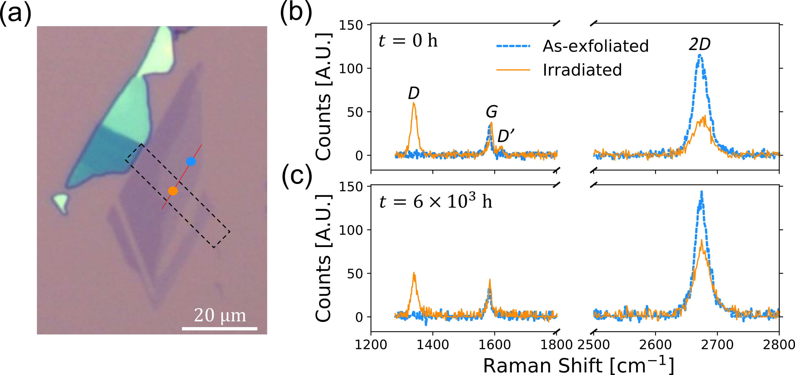
The sample, shown in Figure 1a, was characterized before the irradiation to confirm the high quality of the monolayer graphene crystal (See SI). The sample was then irradiated as described in methods to induce defects in the lattice. Figure 1b shows the comparison between Raman spectra collected on irradiated and as-exfoliated graphene right after the exposure to the e-beam (). The spectrum collected on the as-exfoliated part is very similar to the one collected on pristine graphene (Figure S4), demonstrating that the crystal lattice of the unexposed area is not affected by the irradiation process. Instead, the spectrum of irradiated graphene features the typical disordered graphene fingerprint, i.e. a quenched peak and a peak higher than the peak [45, 46]. Also, the peak is blue-shifted with respect to the same peak on pristine graphene and a peak is visible. See Table S3 for the values obtained from the Lorentzian fits of the peaks. Such a difference in the spectra confirms the presence of defects locally induced by the irradiation. To quantify such defects, the ratio of the intensities of the and peaks is used. A ratio of is observed at . This ratio can be linked to the density of defects in the lattice by the formula [47]:
| (1) |
where is the Raman laser excitation energy. By using this formula, the observed ratio results in a starting density . Figure 1c shows the comparison between the Raman spectra collected on the same irradiated and as-exfoliated graphene after a time from the exposition. The signal collected on as-exfoliated graphene is comparable to the spectrum at , showing that pristine graphene did not deteriorate during time. Conversely, the spectrum of irradiated graphene shows a reduction of the peak and a partial restoration of the intensity of the peak. The peak is shifted closer to the as-exfoliated condition and the peak is reduced (see Table S3). The intensity ratio is , corresponding to a density of defects at the end of the experiment [47].
To study the time evolution at room temperature of the induced defects, different Raman measurements were performed over time on the device. Figure 2a shows the ratios extracted from spectra taken at different time on the irradiated part of the flake. The corresponding values of are reported on the right -axis. Two different phases of the evolution can be distinguished: a first phase (from h to h in Fig. 2a), where the density of defects is almost constant over a timescale of 10 hours, and a second phase (from h to h), in which a reduction of the density is observed in a timescale of hours, suggesting the occurrence of a room temperature healing process. To better quantify the timescale of the reduction, the data were fitted with an exponential decay (see SI and Figure 2a). A time constant of h was extracted, while the percentage of defects that heal during the evolution is quantified to be as high as .
In the case under analysis, the defect density is low enough to still consider graphene as nanocrystalline [48, 49]. In such regime, the positions and of the and peaks can be correlated to extract information on doping and strain of the examined crystal structure (Figure 2b) [50]. At time , the irradiated part shows a higher doping with respect to the as-exfoliated area. This is expected due to charge impurities accumulated in the substrate during the exposition [51]. Also, the defected area shows a higher tensile strain than the as-exfoliated area, due to the presence of defects [52, 53].
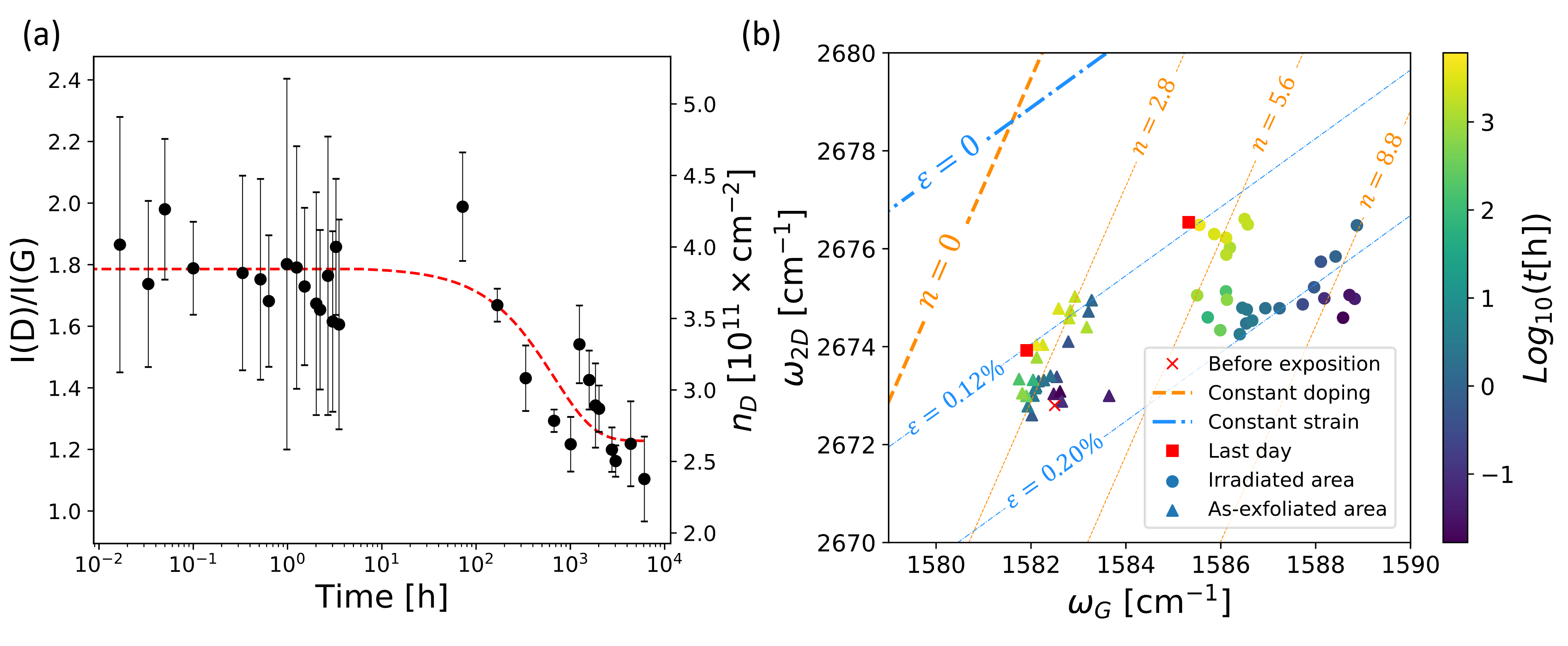
Instead, the data collected on the as-exfoliated area are comparable to the values obtained on the crystal before irradiation (red cross in Figure 2b). Importantly, the evolution over time of the two areas is different. In the irradiated area, two temporal phases can be isolated as in Figure 2a. During the first 10 hours, the doping decreases from a value to . This change is attributed to the decay of the charge impurities accumulated in the substrate during the exposition. Indeed, charge impurities in have been observed to last up to few hours ( h) after the irradiation [54]. After the decrease in doping, the crystal lattice relaxes its tensile strain from a value to a value in a timescale of hours. During the relaxation, the doping change is negligible. Instead, the as-exfoliated area follows a different path. First, the evolution cannot be divided into two distinguishable phases as in the case of the irradiated area. Second, the strain in the lattice decreases over time while the doping remains constant at . The two examined parts eventually reach a condition where both share the same value of strain .
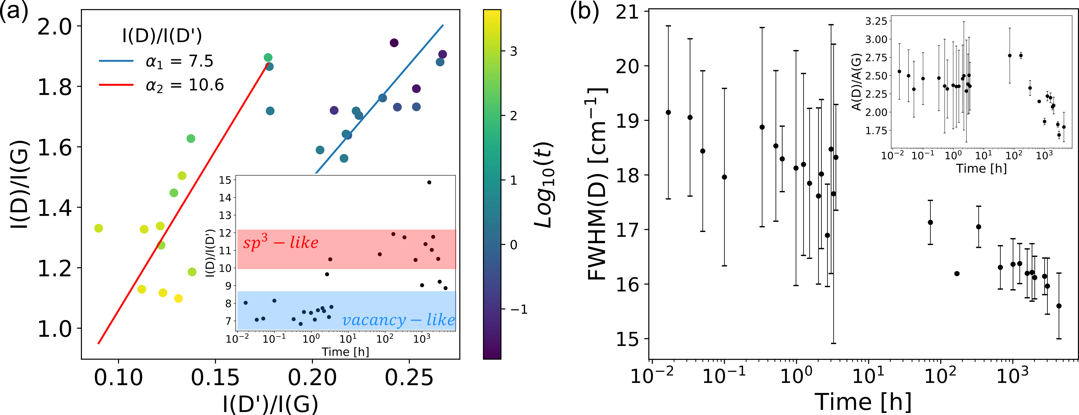
To understand more in depth the mechanism driving the observed time evolution, we studied the nature of the defects by examining the intensities of and peaks. A plot of the intensities of the two peaks normalized on the relative peak is shown in Figure 3a. A linear correlation between the two parameters is visible with a coefficient . In general, this ratio gives information on the statistical composition of the defect population [55]. Interestingly, the two phases identified in the time evolution are characterized by two distinct -coefficients extracted by linear fits, also shown in Fig 3a. The first phase of the evolution is characterized by a coefficient . In the second phase, the extracted coefficient is . Assuming the model proposed in Ref. [55] for the -coefficient, the value of indicates that, right after the exposition, the defect population is mainly composed of vacancy-like sites, such as borders and holes in the lattice. In the case of electron-nucleus collisions, C atoms are displaced out of the graphene lattice eventually creating atomic vacancies when incident electrons have energy larger than 86 keV, i.e. when the transferred energy exceeds the knock-on threshold energy [56]. Nevertheless, lattice disruption are expected to occur also at 20-30 keV due to cumulative dose effect in continuous irradiation [26, 56] or due to electrostatic fields caused by charged puddles generated by the irradiation in case of substrates with dielectric films, such as SiO2/Si [57, 58, 59].
After the creation of the defects, vacancies-rich defects remain in the first -hour phase (blue-shaded area in the inset of Figure 3a). Then, the coefficient increases up to the value. This indicates a change of the population towards a majority of -like defects (red-shaded area in the inset of Figure 3a). In addition, air contaminants can bond to the dangling bonds at the boundaries of the holes, thus changing the hybridization of the involved carbon atoms. This process, combined with the behaviour of shown in Figure 2a, might suggest that the defect density does not decrease and the healing process is in fact absent. Indeed, if many contaminants bonded to the carbon dangling bonds, the measured intensity of the peak would be quenched by the presence of such molecules [48]. Hence, the density of defects would not actually decrease. Moreover, the full width at half maximum of the peak would increase, because of the larger energy spectrum of the bonds between carbon and different external molecules [48]. Albeit some external molecules may be bonded to the defective sites due to their enhanced chemical reactivity, in our sample narrows with time. As shown in Figure 3b, the width of the D peak decreases from to a final value of . Such a decrease implies that the area below the measured peak diminishes over time, as shown in the inset of Figure 3b, and thus, that a decrease of the density of defects in the crystal takes place. Consequently, the evolution, combined with the partial 2D peak restoration (see SI Figure S5), confirms the presence of a healing process.
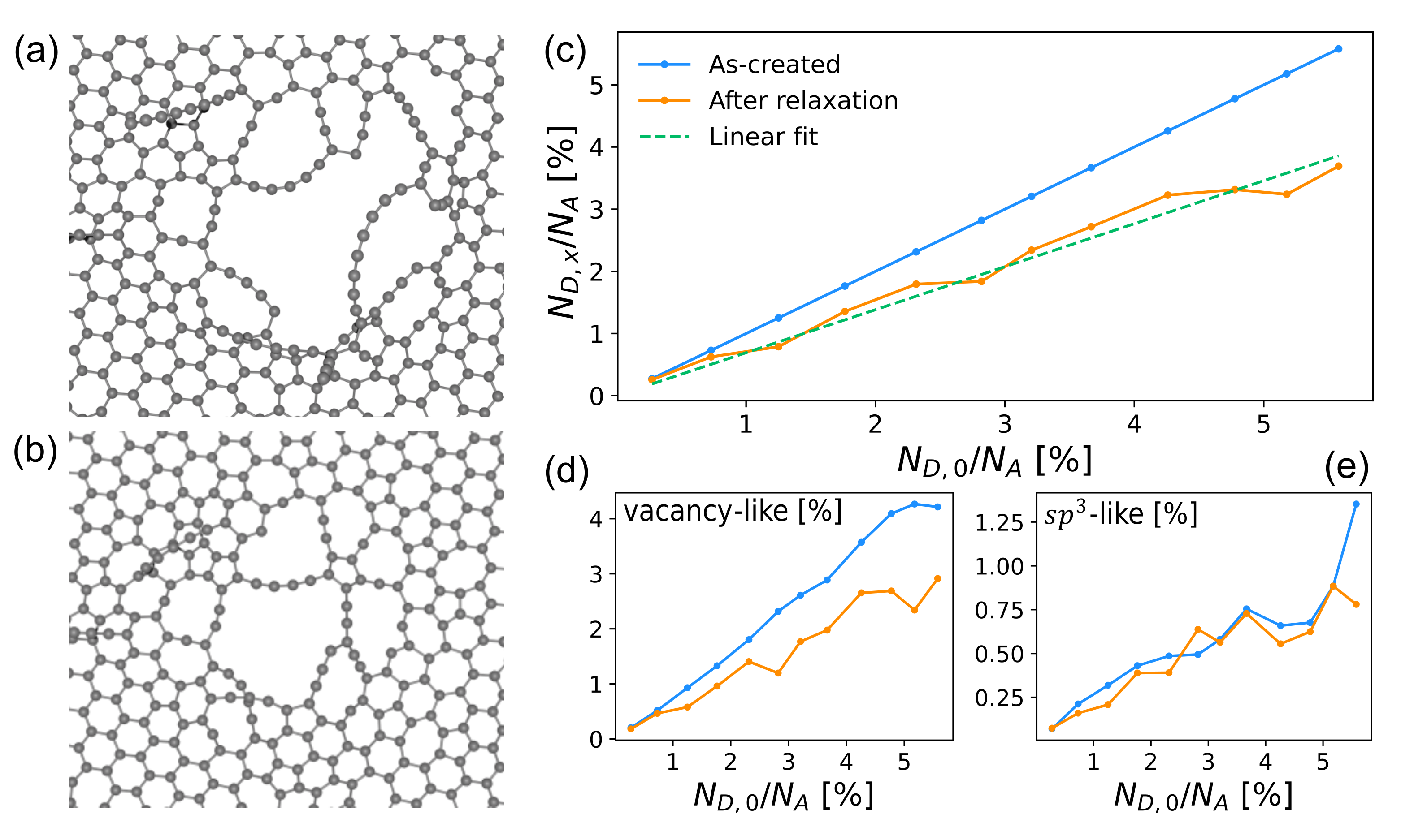
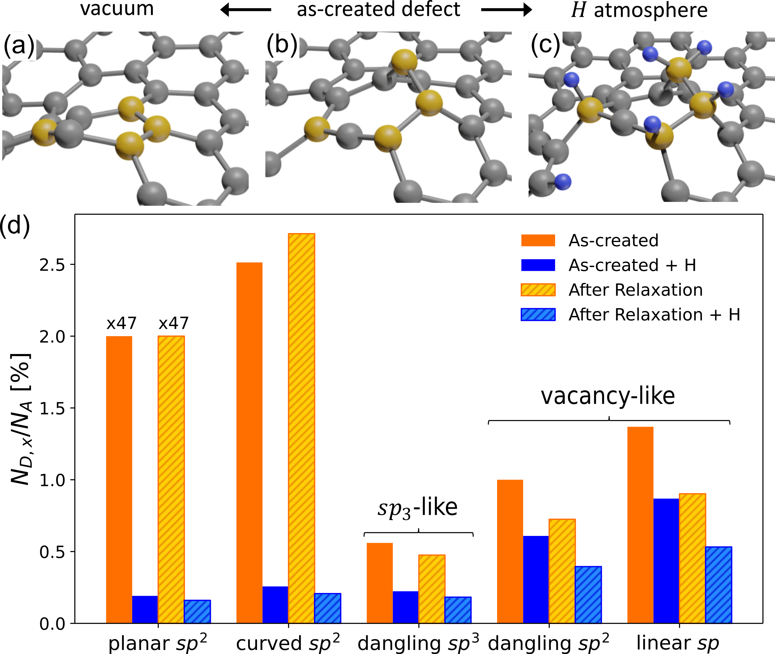
To explain the observed behaviour on the atomic scale, MD simulations were performed to mimic low-energy EBI (see Methods section). Figure 4a and b show an example of such created defected sites right after the end of the irradiation process and after relaxation, respectively. As-created defects (Figure 4a) appear like irregular defects composed of vacancies, carbon polygons and carbon chains, rather than a well defined nanopore. During the irradiation, the planar graphene structure is partially converted into a corrugated lattice with , , and unsaturated C atoms (see Figure S6 in SI for further examples). During the relaxation, unsaturated atoms tend to be saturated by other C atoms. Thus, the defected site reduces in lateral size and parts of the crystal lattice are reconstructed (Figure 4b). Several equivalent systems were irradiated to create different defected sites with increasing number of amorphous C atomic structures. Figure 4c shows the percentage of defected atoms () over the total number of atoms in the systems () (see SI) before () and after the relaxation () in vacuum as a function of the percentage of defected atoms in the as-created defected systems (). The blue line referring to the as-created conditions can be used as a reference. Interestingly, () shows a linear behaviour (orange curve in Figure 4c) with an extracted linear coefficient . This suggests that the healing process depends on the size of the defected area but, in average, the fraction of healed defects is at least about of the starting distorted atoms, in good agreement with the experimental observations. As seen in Figure 3a, vacancy-like defects can be distinguished from -like defects by a different Raman activity. However, a more detailed definition can be given from the atomistic point of view. In fact, vacancy-like defects and -like defects are composed by different kinds of C atoms, which can be identified in the simulations (see SI). The first group includes atoms at the border of large holes or linked to linear chains, like the one represented in Figure 4a. The second group includes -hybridized atoms and quantifies the deviation from the planarity of -hybridized C in the lattice.
The results on the simulated evolution of these two groups allow to better understand the experimentally observed healing process, i.e. the change from vacancy-rich to -like population. The number of vacancy-like defects decreases during relaxation as the hole partially refills with hexagonal rings (Figure 4d), while the -like population remains constant on average (Figure 4d). This behaviour can be explained as follows. On the one hand, the atoms with dangling bonds that are at the edge of the hole and the linear carbon chains, i.e. the vacancy-like atoms, are prone to react towards saturation. Hence, by saturating the dangling bonds, the lattice is recovered and the structure is locally stabilized. Such a mechanism arises from the simultaneous availability of dangling bonds and movable linear C chains, which are intrinsic features of the created defects, and represent the driving force for the reconstruction of graphene. On the other hand, even if some distorted atoms can relax towards a more planar disposition, other surrounding atoms may rearrange during the evolution as an effect of the reconstruction (see Figure 5a and b), thus explaining why the -like population does not change on average.
The simulations in vacuum well reproduce the healing trends that are experimentally observed at microscopic level in ambient air. This can be explained by the fact that the lattice reconstruction involves defects with different nature, which evolve differently with time. In particular, when exposed to ambient air, defective sites may chemically react with airborne contaminants due to the enhanced reactivity[6, 60]. Indeed, we observed a larger charge doping in the irradiated areas compared to the pristine graphene. However, the probability of chemical bonding between defects and airborne contaminants is modest at standard temperature and pressure [61], as also demonstrated by the almost constant charge doping and the narrowing with time in our samples (see Figure 2a and Figure 3b, respectively). Consequently, the bonding of the defects with external molecules is not an immediate mechanism. This gives rise to a slow saturation process of the electron-induced dangling bonds, allowing the vacancy-like defects to be reconstructed during time.
To deeply investigate the role of the chemical reactive sites in the healing process, we carried out additional MD simulations and studied the graphene reactivity in the presence of defects. The systems were subjected to tempering cycles in the presence of atomic hydrogen (see Computational methods section). We employed atomic hydrogen in order to probe the reactivity of the defected sites with a very active species. As a first test, pristine graphene was simulated in H atmosphere. No atoms bonded to the surface (see video in SI), thus demonstrating that pristine graphene is chemically inert in the chosen condition (see Methods and SI). Instead, the defected sites interacted with H, yielding different outcomes. For example, if vacancy-like atoms are saturated by an H atom, the configuration likely stabilizes the hybridization and that particular defect stops the healing mechanism observed in vacuum. If -like atoms are saturated by H atoms, the distorted carbon atoms change their hybridization to and the lattice out-of plane distortions convert into stable tertiary C atoms bound to H, as shown in Figure 5b and c. In general, H contamination of the as-created systems pointed out that the reactivity of planar is not zero as in pristine (i.e. non-defected) graphene (see solid bars in Figure 5d). This implies that defects affect the reactivity of the system also at relatively longer distances. Curved and -like atoms show an improved reactivity [62, 63], while dangling bonds show the highest reactivity (dangling and linear in Figure 5d). Besides, it is worth noting that, even when the systems were subjected to a strong chemical attack, the chemical saturation occurred gradually and some dangling bonds remain unsaturated by atomic H even after few aging cycles (see Figure 5d). Consequently, these results indicate that, even in the worst case scenario, i.e. the presence of high reactive species, the evolution of the system is a concurrency of the reconstruction mechanism of the lattice, which happens as if it were in vacuum, and the creation of distorted sites that can interact with possible contaminants and is responsible for the change in nature of the defects during time observed in the experiment (see Figure 3a).
For applications employing the defected sites in the functionalization of graphene, it is important that the improved reactivity is preserved over time. To test this, hydrogen attack was performed over the relaxed systems as well (textured bars in Figure 5d). After relaxation, the vacancy-like population decreases and consequently decreases the amount of saturated vacancy-like defects. Also in this case, the -like population remains constant during relaxation, guaranteeing an improved reactivity also after a long time.
3 Conclusions
The evolution over time of defects in a graphene flake was studied via both micro-Raman spectroscopy and MD simulations. Experimentally, the structural defects were patterned by low-energy EBI in an exfoliated graphene sheet. During the first h after the irradiation, the charge accumulated in the substrate due to the exposure relaxes and the local doping of graphene decreases, but the crystal modifications are otherwise unaffected and maintain the highest density value that is determined by the exposure parameters ().
On a much longer timescale of h, the actual crystal partially recovers and a stable defective state is maintained. This stable state is reached after a partial reconstruction of of the defects with a consequent local tensile strain relaxation, pointing out that graphene can rebuild its lattice when exposed to ambient air at room temperature without any specific healing treatment. The MD simulations results supported the observed reconstruction of the defected sites for at least of the distorted atoms in vacuum. Moreover, the simulations showed that the induced defects are composite sites with vacancies and complex amorphous C structures and not well defined nanoholes. In fact, the experiment shows that vacancy-like defects are the main component of the defected site right after the exposure. Thereafter, such vacancy-like population decreases over time due to the reconstruction and to the possible saturation of the dangling bonds with airborne contaminants, while the -like population is on average constant over time due to rearrangements in the lattice. Interestingly, the simulations also showed that curved atoms are generated by the irradiation and preserved during aging. Alike -like atoms, curved atoms are more reactive than planar carbon [64] and curved graphene has been reported in the literature to be a suitable substrate for H chemisorption [62, 63]. Therefore, the experiment combined with simulations highlighted that, when evolving during time, the modifications of the defected sites are a combination of self-reconstruction of the lattice and creation of reactive sites that promote the chemical interactions in case of defects-airborne contaminant collisions. Such a process occurs on a long timescale because defects must overcome an energy barrier to recombine in the crystal [5] and the probability of collision with airborne contaminants is modest [61].
In summary, the presented work shows that the nature and density of defected sites created by low-energy EBI evolve during time at room temperature and in ambient air conditions. Our results are relevant when dealing with nanoelectronic devices, as they establish the operability timescale for applications. Moreover, when designing the device, the aging of the defective state, and thus the modification of the altered electronics properties, must be taken into account, even when the device is kept under vacuum. Indeed, the highest defective state lasts for a too limited time (less then one day). Then, the system undergoes a general properties modification for more than one month, until it reaches a less defective but stable state, which is more suitable for long-lasting devices applications.
A possible solution to have more stable as-created defects may be encapsulating the graphene sheet. However, additional investigation is necessary when considering this system, as the defect healing may still be non-negligible and its dynamics may be different. Finally, this work points out that defective graphene has chemical activity that lasts during time. The presented complete rationalization of the different self-healing paths and the study of the chemical reactivity of the irradiation-induced defects also provide the conceptual tools to develop advanced chemical functionalization strategies to build novel graphene-based devices for energy storage, sensing and catalysis.
Materials and methods
Fabrication and characterization
The employed substrate is a boron-doped wafer with 300 nm of thermally-grown on top. The substrate was cleaned by oxygen plasma at 100 W for 5 minutes to remove organic residues on its surface. Graphene flakes were deposited on the substrate by micro-mechanical exfoliation of highly oriented pyrolytic graphite.
Defects were induced on part of a graphene flake by irradiating with electrons accelerated at 20 keV. The defected area was precisely targeted by a SEM driven by a pattern generator, and is 6 long and as wide as the graphene flake (see Figure 1a). The e-beam was set to output a current of about 0.15 nA and was then scanned with a step-size of 0.1 . The e-beam delivered a dose of 40 , resulting in a dwell-time of 30 ms.The irradiation was carried out at the base operational vacuum of the SEM chamber, which is of the order of mbar. The sample was also left to degas in vacuum inside the SEM chamber for one night. This precaution reduces at the minimum the presence of undesired contaminants during the processing. Additionally, the irradiation conditions (i.e. chamber vacuum and exposure parameters) guarantee a negligible deposition of a carbonaceous contaminant layer [65].
The induced defects were studied by micro-Raman spectroscopy in ambient air. The flake was scanned by a laser beam at 532 nm with 100x objective, giving a lateral resolution . The laser delivered a power of 118 . A power so low was chosen to exclude any possible laser heating of the lattice, which could give contribution to the healing of the defects. Different measurements were taken in a temporal span of 250 days to study the time evolution of the defects. Each measurement consisted of line scans of the flake taken along the line depicted in Figure 1a. The signal collected on the defected part of the flake was isolated from the one collected on the pristine part via software. We checked with an automated script the presence of the D peak and averaged over the extracted points. Experimental errors were then represented by the standard deviation of the data from the average. The signal collected each time on the pristine part of the graphene flake was analyzed following the same method and used as a reference.
Computational methods
All calculations were performed with the LAMMPS program [66]. Visual inspections of molecular dynamics (MD) trajectories, post analysis and figures were performed with VMD1.9.3 [67]. The systems under study consisted of two layers of graphene, each placed on the two surfaces of an amorphous plate (, see Figure S1) and treated as periodic. The chosen box is a triclinic cell with nm, nm; . The atomic interactions between the carbon atoms (C–C) in graphene and an hydrogen atom, where present, were treated with ReaxFF [36, 37]. Interactions between graphene or H and were described by using Lennard-Jones potentials with the parameters derived from CHARMM force field [68] (see SI). Further details about MD simulations can be found in SI. EBI at 20 keV was simulated exploiting the primary knock-out atoms (PKAs) method in the framework of MD simulation. A total of 38 equivalent systems were subjected to electron irradiation, thus generating 76 different defective graphene lattices (see SI, Figure S6). These irradiated systems were then subjected to a chemical attack by atomic hydrogen and a tempering/annealing procedure in vacuum by employing MD simulations. The chemical attack was performed by heating the system to 800 K and cooling it to 300 K in 10 ps 6 times in the presence of 1800 H atoms in the simulation box. The tempering/annealing procedure in vacuum was carried out by employing 10 cycles in which each system was heated to 3000 K and cooled to 300 K. Each cycle was 10 ps long. The relaxed systems were then subjected to the same H chemical attack procedure.
Authorship statement
Nicola Melchioni: Data Curation, Formal Analysis, Investigation, Writing – Original Draft
Luca Bellucci: Data Curation (MD Simulations), Funding acquisition, Investigation, Methodology (MD Simulations), Writing – Review&Editing
Alessandro Tredicucci: Funding acquisition, Writing – Review&Editing
Federica Bianco: Conceptualization, Data Curation, Funding acquisition, Investigation, Methodology, Writing – Review&Editing
Supporting Information
Additional experimental details, computational and analysis methods (PDF); Movie of the simulated structures (MPG)
Data Availability
All the data are available upon request to the corresponding authors.
Acknowledgments
This research was partially founded by EU-H2020 FETPROACT LESGO (Agreement No. 952068) and by "MONstre-2D" Project under the PRIN 2017 call and "q-LIMA" Project under the PRIN 2020 call granted by the Italian Ministry of University and Research. The authors wish to acknowledge Dr. C. Coletti from Istituto Italiano di Tecnologia for the access to micro-Raman facility.
References
- [1] Xiaoming Li et al. “Carbon and Graphene Quantum Dots for Optoelectronic and Energy Devices: A Review” In Advanced Functional Materials 25.31, 2015, pp. 4929–4947 DOI: https://doi.org/10.1002/adfm.201501250
- [2] A.G. Olabi, M.A Abdelkareem, T. Wilberforce and E.T. Sayed “Application of graphene in energy storage device - A review” In Renewable and Sustainable Energy Reviews 135, 2021, pp. 110026
- [3] Pravin O. Patil et al. “Graphene-based nanocomposites for sensitivity enhancement of surface plasmon resonance sensor for biological and chemical sensing: A review” In Biosensors and Bioelectronics 139, 2019, pp. 111324 DOI: https://doi.org/10.1016/j.bios.2019.111324
- [4] Albert Boretti et al. “Outlook for graphene-based desalination membranes” In npj Clean Water 1.5, 2018
- [5] F. Banhart, J. Kotakoski and A.V. Krasheninnikov “Structural Defects in Graphene” In ACS Nano 5.1, 2011, pp. 26–41
- [6] L. Liu, M. Qing, Y. Wang and S. Chen “Defects in Graphene: Generation, Healing, and Their Effects on the Properties of Graphene: A Review” In Journal of Materials Science & Technology 31.6, 2015, pp. 599–606
- [7] Gao Yang, Lihua Li, Wing Bun Lee and Man Cheung Ng “Structure of graphene and its disorders: a review” In Science and Technology of Advanced Materials 19.1 Taylor & Francis, 2018, pp. 613–648 DOI: 10.1080/14686996.2018.1494493
- [8] D.. Boukhvalov and M.. Katsnelson “Chemical functionalization of graphene with defects” In Nano Letters 8.12, 2008, pp. 4373–4379 DOI: 10.1021/nl802234n
- [9] Sandra C. Hernández et al. “Controlling the local chemical reactivity of graphene through spatial functionalization” In Carbon 60, 2013, pp. 84–93 DOI: 10.1016/j.carbon.2013.03.059
- [10] Xiao-Liang Ye et al. “Quantifying defect-enhanced chemical functionalization of single-layer graphene and its application in supramolecular assembly” In J. Mater. Chem. A 5 The Royal Society of Chemistry, 2017, pp. 24257–24262 DOI: 10.1039/C7TA07612F
- [11] G. Lee et al. “Defect-engineered graphene chemical sensors with ultrahigh sensitivity” In Phys. Chem. Chem. Phys. 18, 2016, pp. 14198–14204
- [12] Gagus Ketut Sunnardianto et al. “Efficient hydrogen storage in defective graphene and its mechanical stability: A combined density functional theory and molecular dynamics simulation study” In International Journal of Hydrogen Energy 46.7, 2021, pp. 5485–5494 DOI: https://doi.org/10.1016/j.ijhydene.2020.11.068
- [13] A. Bhattacharya, S. Bhattacharya, C. Majumder and G.. Das “Transition-Metal Decoration Enhanced Room-Temperature Hydrogen Storage in a Defect-Modulated Graphene Sheet” In The Journal of Physical Chemistry C 114.22, 2010, pp. 10297–10301 DOI: 10.1021/jp100230c
- [14] Zhicong Liang, Xiaofeng Fan, Weitao Zheng and David J. Singh “Adsorption and Formation of Small Na Clusters on Pristine and Double-Vacancy Graphene for Anodes of Na-Ion Batteries” PMID: 28474877 In ACS Applied Materials & Interfaces 9.20, 2017, pp. 17076–17084 DOI: 10.1021/acsami.7b02972
- [15] R. Akilan et al. “Modeling of 2-D hydrogen-edge capped defected & boron-doped defected graphene sheets for the adsorption of CO2, SO2 towards energy harvesting applications” In Applied Surface Science 463, 2019, pp. 596–609 DOI: https://doi.org/10.1016/j.apsusc.2018.08.179
- [16] G. Liu, D. Teweldebrhan and A.. Balandin “Tuning of graphene properties via controlled exposure to electron beams” In IEEE Transactions on Nanotechnology 10.4, 2011, pp. 865–870 DOI: 10.1109/TNANO.2010.2087391
- [17] Hoda Malekpour et al. “Thermal conductivity of graphene with defects induced by electron beam irradiation” In Nanoscale 8 The Royal Society of Chemistry, 2016, pp. 14608–14616 DOI: 10.1039/C6NR03470E
- [18] Yuki Anno et al. “Enhancement of graphene thermoelectric performance through defect engineering” In 2D Materials 4.2 IOP Publishing, 2017, pp. 025019 DOI: 10.1088/2053-1583/aa57fc
- [19] Qi Han et al. “Highly sensitive hot electron bolometer baased on disordered graphene” In Scientific Reports, 2013 DOI: 10.1038/srep03533
- [20] Guanxiong Liu, Desalegne Teweldebrhan and Alexander A. Balandin “Tuning of Graphene Properties via Controlled Exposure to Electron Beams” In IEEE Transactions on Nanotechnology 10.4, 2011, pp. 865–870 DOI: 10.1109/TNANO.2010.2087391
- [21] Li Tao et al. “Modification on Single-Layer Graphene Induced by Low-Energy Electron-Beam Irradiation” In The Journal of Physical Chemistry C 117.19, 2013, pp. 10079–10085 DOI: 10.1021/jp312075v
- [22] Litao Sun, Florian Banhart and Jamie Warner “Two-dimensional materials under electron irradiation” In MRS Bulletin 40, 2015, pp. 29–37 DOI: 10.1557/mrs.2014.303
- [23] Katsuhisa Murakami, Takuya Kadowaki and Jun-ichi Fujita “Damage and strain in single-layer graphene induced by very-low-energy electron-beam irradiation” In Applied Physics Letters 102.043111, 2013 DOI: 10.1063/1.4790388
- [24] Hengfei Gu et al. “Considerable knock-on displacement of metal atoms under a low energy electron beam” In Scientific Reports 7.184, 2017 DOI: 10.1038/s41598-017-00251-3
- [25] Luca Basta, Aldo Moscardini, Stefano Veronesi and Federica Bianco “Substrate surface effects on electron-irradiated graphene” In Surfaces and Interfaces 28, 2022, pp. 101694 DOI: https://doi.org/10.1016/j.surfin.2021.101694
- [26] Xin Wu “Influence of Particle Beam Irradiation on the Structure and properties of graphene”, Springer Theses Springer Singapore, 2018 DOI: 10.1007/978-981-10-6457-9
- [27] D. Teweldebrhan and A.A. Balandin “Modification of graphene properties due to electron-beam irradiation” In Applied Phisics Letter 94.013101, 2009 DOI: 10.1063/1.3062851
- [28] Issai Shlimak and Moshe Kaveh “Raman Spectra in Irradiated Graphene: Line Broadening, Effects of Aging and Annealing” In Graphene 9, 2020, pp. 13–28
- [29] Li Liu et al. “Direct observation of atomic scale graphitic layer growth” In Nano Lett. 8.7, 2008, pp. 1872–1878 DOI: https://doi.org/10.1021/nl0804046
- [30] B. Wang and S.. Pantelides “Controllable healing of defects and nitrogen doping of graphene by CO and NO molecules” In Phys. Rev. B 83, 2011, pp. 245403
- [31] L. Tsetseris and S.T. Pantelides “Adatom complexes and self-healing mechanisms on graphene and single-wall carbon nanotubes” In Carbon 47.3, 2009, pp. 901–908 DOI: https://doi.org/10.1016/j.carbon.2008.12.002
- [32] Recep Zan, Quentin M. Ramasse, Ursel Bangert and Konstantin S. Novoselov “Graphene Reknits Its Holes” In Nano Letters 12.8, 2012, pp. 3936–3940
- [33] Ahmad Ehteshamul Islam et al. “Defect engineering of graphene using electron-beam chemistry with radiolyzed water” In Carbon 166, 2020, pp. 446–455
- [34] T.P. Senftle et al. “The ReaxFF reactive force-field: development, applications and future directions” In npj Computational Materials 2.15011, 2016
- [35] L.C. Lin and J.C. Grossman “Atomistic understanding of reduced graphene oxide as an ultrathin-film nanoporous membrane for separations” In Nature Communications 6.8335, 2015
- [36] Adri CT Van Duin, Siddharth Dasgupta, Francois Lorant and William A Goddard “ReaxFF: a reactive force field for hydrocarbons” In The Journal of Physical Chemistry A 105.41 ACS Publications, 2001, pp. 9396–9409
- [37] Malgorzata Kowalik et al. “Atomistic scale analysis of the carbonization process for C/H/O/N-based polymers with the ReaxFF reactive force field” In The Journal of Physical Chemistry B 123.25 ACS Publications, 2019, pp. 5357–5367
- [38] Malgorzata Kowalik et al. “Atomistic-Scale Simulations on Graphene Bending Near a Copper Surface” In Catalysts 11.2 Multidisciplinary Digital Publishing Institute, 2021, pp. 208
- [39] Alexander J. Marsden et al. “From graphene to graphene oxide: the importance of extended topological defects” In Phys. Chem. Chem. Phys. 24 The Royal Society of Chemistry, 2022, pp. 2318–2331 DOI: 10.1039/D1CP04316A
- [40] Sehmus Ozden et al. “Egg protein derived ultralightweight hybrid monolithic aerogel for water purification” In Materials Today 59, 2022, pp. 46–55 DOI: 10.1016/j.mattod.2022.08.001
- [41] Jun Xia et al. “Transformation between divacancy defects induced by an energy pulse in graphene” In Nanotechnology 27.27 IOP Publishing, 2016, pp. 274004
- [42] Inkook Jang, Susan B Sinnott, Daniel Danailov and Pawel Keblinski “Molecular dynamics simulation study of carbon nanotube welding under electron beam irradiation” In Nano Letters 4.1 ACS Publications, 2004, pp. 109–114
- [43] Yoshiki Asayama et al. “Molecular dynamics study of the structural modification of graphene by electron irradiation” In Journal of Vacuum Science & Technology B, Nanotechnology and Microelectronics: Materials, Processing, Measurement, and Phenomena 30.6 American Vacuum Society, 2012, pp. 06FJ02
- [44] Shogo Kida et al. “Correlation between electron-irradiation defects and applied stress in graphene: A molecular dynamics study” In Journal of Vacuum Science & Technology A: Vacuum, Surfaces, and Films 33.5 American Vacuum Society, 2015, pp. 05E127
- [45] B. Krauss et al. “Laser-induced disassembly of a graphene single crystal into a nanocrystalline network” In Phys. Rev. B 79 American Physical Society, 2009, pp. 165428 DOI: 10.1103/PhysRevB.79.165428
- [46] Jiang-Bin Wu et al. “Raman spectroscopy of graphene-based materials and its applications in related devices” In Chem. Soc. Rev. 47 The Royal Society of Chemistry, 2018, pp. 1822–1873 DOI: 10.1039/C6CS00915H
- [47] Matteo Bruna et al. “Doping Dependence of the Raman Spectrum of Defected Graphene” In ACS Nano 8.7, 2014, pp. 7432–7441
- [48] Axel Eckmann et al. “Raman study on defective graphene: Effect of the excitation energy, type, and amount of defects” In Phys. Rev. B 88, 2013, pp. 035426 DOI: 10.1103/PhysRevB.88.035426
- [49] M.. Lucchese et al. “Quantifying ion-induced defects and Raman relaxation length in graphene” In Carbon, 2010, pp. 1592–1597 DOI: https://doi.org/10.1016/j.carbon.2009.12.057
- [50] Ji Eun Lee et al. “Optical separation of mechanical strain from charge doping in graphene” In Nat. Comm. 8.7, 2012, pp. 7432–7441
- [51] H. Park et al. “Characterization of boron charge traps at the interface of Si/SiO2 using second harmonic generation” In Applied Physics Letters 95.6, 2009, pp. 062102
- [52] Jean-Marc Leyssale and Gérard L. Vignoles “A Large-Scale Molecular Dynamics Study of the Divacancy Defect in Graphene” In The Journal of Physical Chemistry C 118.15, 2014, pp. 8200–8216 DOI: 10.1021/jp501028n
- [53] Nils Blanc et al. “Strains Induced by Point Defects in Graphene on a Metal” In Phys. Rev. Lett. 111 American Physical Society, 2013, pp. 085501 DOI: 10.1103/PhysRevLett.111.085501
- [54] Kristen M. Burson et al. “Direct Imaging of charged impurity density in common graphene substrates” In Nano Letters 95.6, 2013, pp. 062102
- [55] Axel Eckmann et al. “Probing the Nature of Defects in Graphene by Raman Spectroscopy” PMID: 22764888 In Nano Letters 12.8, 2012, pp. 3925–3930 DOI: 10.1021/nl300901a
- [56] J. Kotakoski and Arkady V. Krasheninnikov “Computational Nanoscience” The Royal Society of Chemistry, 2011, pp. 334–376
- [57] N.R. Guseinov and A.M. Ilyin “Under threshold structural damaging in few-Layer graphene due to middle- and low-energy electron irradiation” In Journal of Materials Science and Engineering A 4 1, 2014, pp. 39–44 DOI: https://10.17265/2161-6213/2014.01.006
- [58] A.M. Ilyin et al. “Bridge-like radiation defects in few-layer graphene” 25th International Conference on Atomic Collisions in Solids (ICACS-25) In Nuclear Instruments and Methods in Physics Research Section B: Beam Interactions with Materials and Atoms 315, 2013, pp. 192–196 DOI: https://doi.org/10.1016/j.nimb.2013.03.058
- [59] N.. Guseinov and A.. Ilyin “Subthreshold Radiation Damage in Few-Layer Graphene Nanostructures Due to Low-Energy Electron Irradiation” In New Approaches in Engineering Research Vol. 10, 2021, pp. 32–40 DOI: 10.9734/bpi/naer/v10/11530D
- [60] Pablo A. Denis and Federico Iribarne “Comparative Study of Defect Reactivity in Graphene” In The Journal of Physical Chemistry C 117.37, 2013, pp. 19048–19055 DOI: 10.1021/jp4061945
- [61] Zhiting Li et al. “Effect of airborne contaminants on the wettability of supported graphene and graphite” In Nature Materials 12, 2013, pp. 925–931 DOI: https://doi.org/10.1038/nmat3709
- [62] Valentina Tozzini and Vittorio Pellegrini “Prospects for hydrogen storage in graphene” In Phys. Chem. Chem. Phys. 15 The Royal Society of Chemistry, 2013, pp. 80–89 DOI: 10.1039/C2CP42538F
- [63] Laura Ciammaruchi et al. “Water splitting of hydrogen chemisorbed in graphene oxide dynamically evolves into a graphane lattice” In Carbon 153, 2019, pp. 234–241 DOI: https://doi.org/10.1016/j.carbon.2019.06.087
- [64] Dimitrios Tasis, Nikos Tagmatarchis, Alberto Bianco and Maurizio Prato “Chemistry of Carbon Nanotubes” PMID: 16522018 In Chemical Reviews 106.3, 2006, pp. 1105–1136 DOI: 10.1021/cr050569o
- [65] J.D. Femi-Oyetoro et al. “Effects of high-dosage focused electron-beam irradiation at energies ≤ 30 keV on graphene on SiO2” In Applied Surface Science 469, 2019, pp. 325–330 DOI: 10.1016/j.apsusc.2018.10.250
- [66] Steve Plimpton “Fast parallel algorithms for short-range molecular dynamics” In Journal of computational physics 117.1 Elsevier, 1995, pp. 1–19
- [67] W. Humphrey, A. Dalke and K. Schulten “VMD: Visual molecular dynamics” In Journal of Molecular Graphics 14.1 Elsevier, 1996, pp. 33–38
- [68] Eduardo R Cruz-Chu, Aleksei Aksimentiev and Klaus Schulten “Water- silica force field for simulating nanodevices” In The Journal of Physical Chemistry B 110.43 ACS Publications, 2006, pp. 21497–21508