Efficient Photonic Integration of Diamond Color Centers and Thin-Film Lithium Niobate
Supplementary Material
††journal: opticajournal††articletype: Research ArticleOn-chip photonic quantum circuits with integrated quantum memories have the potential to radically progress hardware for quantum information processing. In particular, negatively charged group-IV color centers in diamond are promising candidates for quantum memories, as they combine long storage times with excellent optical emission properties and an optically-addressable spin state. However, as a material, diamond lacks many functionalities needed to realize scalable quantum systems. Thin-film lithium niobate (TFLN), in contrast, offers a number of useful photonic nonlinearities, including the electro-optic effect, piezoelectricity, and capabilities for periodically-poled quasi-phase matching. Here, we present highly efficient heterogeneous integration of diamond nanobeams containing negatively charged silicon-vacancy (SiV) centers with TFLN waveguides. We observe greater than 90% transmission efficiency between the diamond nanobeam and TFLN waveguide on average across multiple measurements. By comparing saturation signal levels between confocal and integrated collection, we determine a -fold increase in photon counts channeled into TFLN waveguides versus that into out-of-plane collection channels. Our results constitute a key step for creating scalable integrated quantum photonic circuits that leverage the advantages of both diamond and TFLN materials.
1 Introduction
Optically addressable solid-state spin qubits are promising building blocks for scalable quantum networking applications [1, 2]. Among these, diamond color center defects are leading candidates for advancing quantum networks. Long-lived 13C nuclear spins in diamond can be harnessed as quantum memories [3, 4], while nitrogen-vacancy centers have been used to demonstrate a multi-node quantum network [5] and quantum teleportation between non-neighboring nodes [6]. Further progress hinges on the efficient integration of color centers into photonic structures to enhance the spin-photon interface without introducing excessive noise [7, 8, 9].
Negatively charged group-IV color centers benefit from structural inversion-symmetry, which, to first-order, shields the local spin structure from nearby electric field noise introduced during nanofabrication[10, 11]. In addition, this family of color centers consistently exhibits high Debye-Waller factors, leading to strong emission into the zero phonon line (ZPL) [12]. These features, in combination with the efficient coupling to nanophotonic cavities, have enabled the demonstration of memory-enhanced quantum communication [13] and the generation of streams of indistinguishable photons [14], rendering SiV centers a prime candidate for quantum networking applications.
However, scalable, monolithic fabrication of diamond photonic integrated circuits (PICs) remains challenging, and complex diamond PICs are precluded by the absence of second-order nonlinearities. To overcome these challenges, heterogeneous integration with mature nanophotonic material platforms is a promising approach [15, 16, 17, 18, 19, 20, 21, 22, 23, 24, 25, 26]. Thin-film lithium niobate (TFLN) offers many advantages over alternative photonic materials via a large nonlinearity. This enables many applications, including strong electro-optic modulation and frequency conversion [27, 28, 29, 30], piezoelectric transduction [31, 32], and periodic poling for quasi-phase matching and nonlinear frequency conversion [33, 34].
Here, we demonstrate efficient heterogeneous integration of a diamond nanobeam featuring incorporated SiV color centers with a TFLN platform using a mechanical pick-and-place approach[35, 36, 37, 15]. By precisely placing double-tapered diamond nanobeams, we demonstrate the bridging of a gapped TFLN waveguide with a diamond-to-LN transmission efficiency of per facet at nm, corresponding to the SiV ZPL wavelength, averaged across multiple measurements. We find a nearly -times improvement in ZPL photon extraction via integrated TFLN collection channels compared to out-of-plane collection from the same device. By taking into consideration grating coupler efficiencies, we can infer an approximately -fold improvement in photon channeling into the TFLN waveguide compared to confocal collection channels. Our results demonstrate a crucial step towards the incorporation of high-quality diamond spin qubits into a scalable nonlinear photonics platform.
2 Results
2.1 Device Fabrication and Transfer
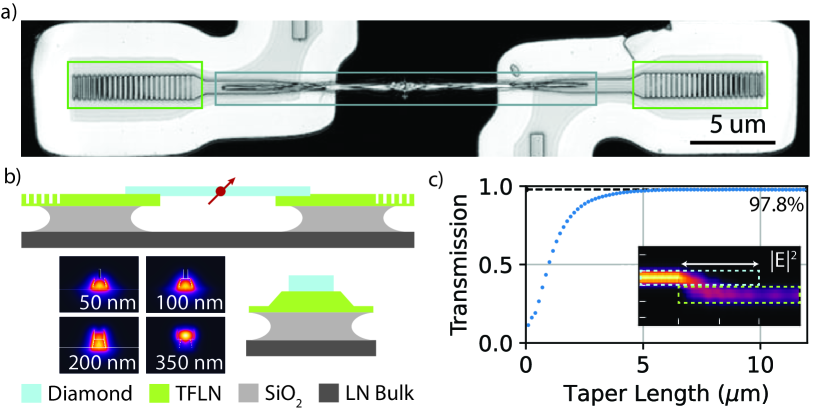
Our device consists of a diamond double-tapered nanobeam with incorporated SiV centers bridging a gapped, undercut TFLN waveguide, imaged in Fig.1(a). The SiV color centers are generated during a chemical vapor deposition (CVD) overgrowth process on a electronic grade bulk single-crystalline diamond. We fabricate the diamond nanobeams using the well-established quasi-isotropic etching technique following the procedures outlined in [38, 39, 40, 35, 11] (see supplemental section S2). Our diamond devices consist of a m long rectangular nanobeam with m tapers at each end, for a total length of m. The nanobeam has a target thickness of nm and its width is tapered from nm to nm at the taper end. The device is anchored to the bulk substrate via a thin tether, around which the nanobeam is widened slightly to reduce scattering effects of the tether on optical transmission.
The TFLN waveguides are fabricated following the techniques demonstrated in [29]. We first pattern a negative resist mask atop a lithium niobate-on-insulator (LNOI) substrate using electron beam lithography. We then employ Ar ion milling to etch the waveguides. A second photolithography mask and ion mill step is used for additional removal of the TFLN slab to expose the buried oxide layer of the LNOI. An additional acid cleaning procedure partially etches this oxide, thereby undercutting the waveguide sockets. The completed TFLN waveguides are approximately nm thick atop an approximately nm thick slab and m wide, which assists in the placement of the diamond nanobeam by allowing for a larger margin of alignment error (Fig.1(b)). The waveguides adiabatically taper down to nm over a length of m. A m gap is left between the two waveguides to serve as a “socket” for a diamond nanobeam. Each waveguide ends in a grating optimized to couple nm light to and from the device (see supplemental section S7).
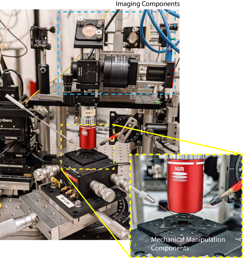
Following fabrication, the diamond nanobeam is transferred via pick-and-place to the TFLN socket. The mechanical transfer process is carried out using a home-built micro-manipulation setup equipped with confocal imaging capabilities and dual tungsten “cat-whisker” needles, each with a nm tip radius. To assist with the mechanical break-off process, the holding tethers are partially cut via focused ion beam (FIB) etching. During transfer, precise orientation of the nanobeam can be controlled with the dual needles, while the LN chip is mounted on a combination of translation and rotation stages. After careful positioning, strong adhesion between the diamond nanobeam and the TFLN via Van der Waals forces allows us to remove the attached needle by pulling it down into the etched trench between the TFLN waveguides. Ultimately, the diamond nanobeam tapers are positioned inversely to the LN “socket” tapers, enabling high-efficiency adiabatic transfer of light between the TFLN waveguide and the diamond nanobeam, as shown in Fig.1(b).
2.2 Optical Characterization of Devices
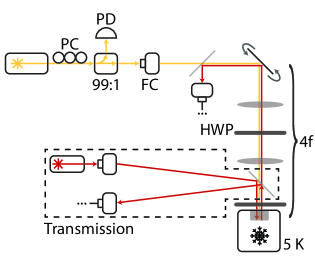
We characterize our device in a closed-cycle Montana cryostat at a temperature of 5 K utilizing a home-built confocal microscopy setup consisting of two distinct access arms. We refer to these collection arms as the confocal and transmission paths. The transmission path can be removed from the apparatus by withdrawing the dichroic just before the cryostat. The full measurement apparatus is schematically depicted in Fig.2.
2.2.1 Transmission
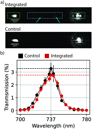
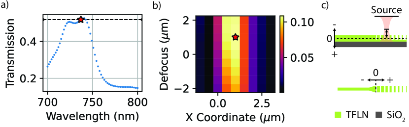
As a first step, we measure transmission through our device, using the TFLN grating couplers to characterize the single-taper transmission efficiency between the diamond and LN. Using the transmission measurement path, we send a narrow-band laser source through one grating coupler and measure the output power through the other. The input laser power is calibrated via a fiber beamsplitter and photodiode at the input. The output transmitted light is coupled into a single mode fiber and routed to a second photodiode. We sweep the Ti:Sapphire laser excitation from nm to nm in intervals of nm, with a separate measurement performed at nm, specifically, as demonstrated in Fig.3(b). Direct transmission through the device at nm is determined to be an uncorrected % from single-mode fiber to single-mode fiber, averaged over four distinct measurements. We then shift the stage to a “control” device, consisting of a fully-connected (i.e., no taper or gap) TFLN waveguide with nominally identical grating couplers, while keeping the excitation and collection alignment fixed. Transmission through the control device (similarly averaged across four distinct measurements) is %, implying a single-mode grating coupler efficiency of %, in agreement with grating coupler simulations (see supplemental section S7). Attributing all additional losses in the device to the adiabatic taper facets, we conclude that each diamond-LN taper has a transmission efficiency of at nm assuming equal taper and grating efficiencies (Fig.3(b) – see supplemental section S5 for additional details on the calibration procedure). This high efficiency is visualized by the lack of significant scattering at both taper contact points to the TFLN and along the diamond nanobeam in Fig.3(a). Importantly, grating couplers are very sensitive to the angle and focal plane of incident light. Therefore, crosstalk and hysteresis in our stage motion can introduce error into this efficiency calibration. However, additional repeated measurements across multiple thermal cycles yield similarly consistent values for taper efficiency. Furthermore, while this is the highest-efficiency device we measured, a second device exhibits an estimated single-taper transmission efficiency of greater than % (see supplemental section S5).
2.2.2 Optical Addressing of SiV
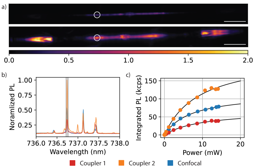
We next perform photoluminescence (PL) measurements on SiV color centers embedded in the diamond waveguide. There are two measurement configurations: one with the excitation and collection co-localized via the confocal path (C/C), and one with confocal excitation but collection through the grating couplers and transmission path (C/CP). Using a homebuilt confocal scanning microscope, we excite color centers off-resonantly at nm and collect the ZPL emission at nm. The resulting PL maps and spectra are presented in Fig.4(a). After locating isolated bright spots in PL, we sweep the optical excitation power and record the PL spectra, comparing the efficiency of SiV emission collected confocally to that collected through the integrated, nanobeam channel. We toggle between confocal and grating coupler collection paths by removing the transmission path dichroic and adjusting only the half-wave plate just before the cryostat. We are careful to make minimal extraneous optical adjustments in order to maintain the validity of any comparisons of the collected signal.
From the PL spectra, we observe a small ensemble of emitters arising from the homogeneous distribution of SiVs throughout the diamond nanobeam. Therefore, for our specific device, we are unable to isolate a single emitter through off-resonant confocal excitation. To quantify photon extraction efficiencies, we thus perform saturation measurements first with the C/CP configuration, then with the C/C configuration, and integrate within the FWHM of identified Lorentzian peaks. As further post filtering, we selectively integrate and fit to the saturation model a representative transition for an SiV center, demarcated by gray in Fig.4(b). We note that we selected a transition which couples favorably to the diamond nanobeam. Errors for photon counts are given by assuming Poissonian photon statistics. We determine a mW ( mW, mW) saturation power and kcps ( kcps, kcps) saturation count rate for C/C configuration (C/CP1, C/CP2). We attribute the slight discrepancy between C/C and C/CP saturation powers to polarization adjustments made between the configurations in order to optimize power delivery to the color center with the removal of the second dichroic mirror [41]. The difference in signal between the two CP configurations can be attributed to preferential emission of the SiV in one direction of the nanobeam due to either angular dipole orientation or positioning in the nanobeam (see supplemental section S6). Most notably, we observe a nearly -times increase in color center photon extraction through the diamond nanobeam and TFLN waveguide grating couplers compared to the confocal channel for collection through CP, indicating extremely high-efficiency diamond-TFLN coupling. Correcting for the grating coupler efficiency , we infer that channeling of SiV photons into the TFLN waveguide is improved by more than -fold when compared to out-of-plane confocal collection through a high-NA objective.
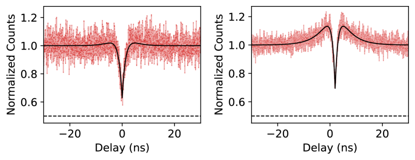
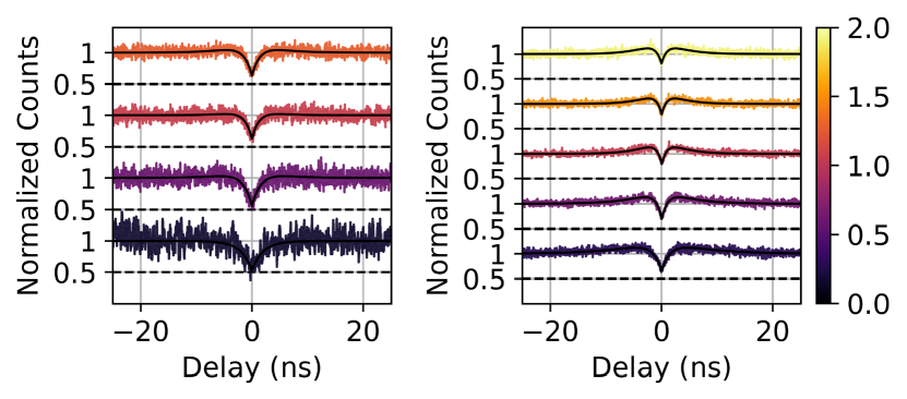
As further evidence of emitter co-localization, we measure auto-correlation of its emission in the C/C configuration using a fiber beamsplitter. We isolate a single emission line with a series of filters, and observe anti-bunching of , indicating emission from an ensemble of emitters within our filtered wavelength region, as shown in Fig.5(a). We then repeat autocorrelation measurements in the C/CP configuration, utilizing our device as an integrated beamsplitter to correlate emission between the two grating couplers. We measure a similar with this approach, depicted in Fig.5(b). The power dependence of the auto-correlation is presented in supplemental section S8.
Lastly, we consider the robustness of the integration to environmental factors. It should be noted that this particular device survived multiple partial and complete thermal cycles. Furthermore, during one such event, the nanobeam fully detached from the TFLN waveguide socket and the pick-and-place apparatus was used to re-position the nanobeam. In all cases, we observed similarly high transmission efficiency. Additional controlled thermal cycling and targeted testing will be necessary to formally characterize this robustness, but repeated transmission measurements suggest a lack of deterioration in device performance.
3 Discussion
Overall, we have demonstrated the photonic integration of diamond color centers with thin-film lithium niobate. Our integration yields very high coupling efficiency of per-facet between the diamond and the TFLN. This translates into a nearly -times increase in off-chip photon collection through integrated channels, and a -fold enhancement in photon channeling into the LN waveguides versus out-of-plane. These metrics enable us to combine the promise of diamond spin qubits with the advantageous optical nonlinearities native to lithium niobate.
Furthermore, the emission count rate is potentially limited by random placement and non-ideal angular orientation of the SiV inside the nanobeam. The homogeneous distribution of color centers within the nanobeam also complicates the probing of single emitter properties in our device. These challenges can be overcome by delta doping and targeted implantation techniques, such as masked or focused ion beam implantation [42, 43, 44, 45]. Furthermore, photon extraction from the emitters into the TFLN waveguide can be enhanced by using resonant photonic structures [46, 47].
A major advantage of selective integration is the possibility for large-scale pre-characterization of diamond nanobeams and emitters, enabling a more deterministic device yield [48]. The transfer process could potentially be fully automated using a combination of machine vision and in situ transmission measurements.
Our device paves the way for high-efficiency emitter collection on TFLN, enabling single-photon experiments that leverage TFLN’s unique properties. We aim to utilize optical nonlinearities in LN for modulating color center emission, thereby demonstrate multi-emitter interference and multiplexing on chip [49]. We further aspire to add additional on-chip capabilities, such as on-chip filters [50] and detectors [51, 52]. On-chip photon routing would enable both the entanglement between several integrated quantum memories and coupling to the same external fiber channel. In combination with recently demonstrated high fiber packaging efficiencies [53], this would enable integrating a large number of quantum memories on the same chip. We also aim to leverage periodic poling in LN to achieve quantum frequency conversion of emitters to the infrared band for integration with the telecom band. These future directions would pave the way towards on-chip heterogeneous platforms linking the excellent optical and coherence properties of solid state spin qubits with the potential of a mature nonlinear photonics platform.
Supplementary information
Supplementary material provided.
Acknowledgments
This material is based upon work supported by the U.S. Department of Energy Office of Science National Quantum Information Science Research Centers as part of the Q-NEXT center. H. Lee acknowledges support from the Stanford Graduate Fellowship. JFH acknowledges support from the NSF GRFP under grant no. DGE-1656518. JG acknowledges support from the Hertz Foundation Graduate Fellowship. SA and VA acknowledge support from the Bloch postdoctoral fellowship in quantum science and engineering from Stanford Quantum Fundamentals, Architecture and Machines initiative (Q-FARM). DR acknowledges support from the Swiss National Science Foundation (project no. P400P2_194424). DR and SA contributed to this work prior to joining AWS. HSS acknowledges support from the Urbanek Family Fellowship. H. Lu and ZXS were supported by the DOE Office of Basic Energy Sciences, Division of Materials Science and Engineering. The authors thank Patrick McQuade, and Alison Rugar for assistance with diamond sample growth. The authors thank Daniil Lukin, Samuel Gyger, Eric Irving Rosenthal, and Luke Qi for helpful discussions regarding sample measurements and data analysis. Work was performed in part in the nano@Stanford labs, which are supported by the National Science Foundation as part of the National Nanotechnology Coordinated Infrastructure under award ECCS-2026822. Part of this work was performed at the Stanford Nano Shared Facilities (SNSF), supported by the National Science Foundation under award ECCS-2026822.
Note. During the writing of this paper we learned of work using similar techniques to calibrate for the transmission efficiencies of adiabatic tapers in a different material platform [54].
Declarations
The authors declare no competing interests.
Data Availability
All data is available from the authors upon reasonable request.
Authors’ Contributions
H. Lee, JG, and DR contributed to the diamond nanobeam design and fabrication. H. Lu, PM, and ZXS, contributed to the diamond sample growth and material preparation. TFLN grating couplers were designed by JFH, and JFH and VA contributed to the TFLN chip fabrication. The adiabatic taper was initially designed and simulated by JMB, DR, and SA, with follow-up simulations conducted by JMB, DR, and JFH. The pick and place setup and transfer of the diamond nanobeam to TFLN was carried out by H. Lee, DR, and JG. Optical measurements of the integrated device were led by H. Lee and assisted by DR, JG, and JFH. The manuscript was prepared by H. Lee, JFH, JG, and DR. Additional support and assistance were contributed by HSS, ASN, and JV. ASN and JV oversaw the experiment and assisted in data interpretation and editing of the manuscript.
References
- [1] D. D. Awschalom, R. Hanson, J. Wrachtrup, and B. B. Zhou, “Quantum technologies with optically interfaced solid-state spins,” \JournalTitleNature Photonics 12, 516–527 (2018).
- [2] M. Atatüre, D. Englund, N. Vamivakas, S.-Y. Lee, and J. Wrachtrup, “Material platforms for spin-based photonic quantum technologies,” \JournalTitleNature Reviews Materials 3, 38–51 (2018).
- [3] M. H. Abobeih, Y. Wang, J. Randall, S. J. Loenen, C. E. Bradley, M. Markham, D. J. Twitchen, B. M. Terhal, and T. H. Taminiau, “Fault-tolerant operation of a logical qubit in a diamond quantum processor,” \JournalTitleNature 606, 884–889 (2022).
- [4] C. E. Bradley, J. Randall, M. H. Abobeih, R. C. Berrevoets, M. J. Degen, M. A. Bakker, M. Markham, D. J. Twitchen, and T. H. Taminiau, “A Ten-Qubit Solid-State Spin Register with Quantum Memory up to One Minute,” \JournalTitlePhysical Review X 9, 031045 (2019).
- [5] M. Pompili, S. L. N. Hermans, S. Baier, H. K. C. Beukers, P. C. Humphreys, R. N. Schouten, R. F. L. Vermeulen, M. J. Tiggelman, L. dos Santos Martins, B. Dirkse, S. Wehner, and R. Hanson, “Realization of a multinode quantum network of remote solid-state qubits,” \JournalTitleScience 372, 259–264 (2021).
- [6] S. L. N. Hermans, M. Pompili, H. K. C. Beukers, S. Baier, J. Borregaard, and R. Hanson, “Qubit teleportation between non-neighbouring nodes in a quantum network,” \JournalTitleNature 605, 663–668 (2022).
- [7] A. Faraon, C. Santori, Z. Huang, V. M. Acosta, and R. G. Beausoleil, “Coupling of nitrogen-vacancy centers to photonic crystal cavities in monocrystalline diamond,” \JournalTitlePhysical Review Letters 109, 33604 (2012).
- [8] D. Riedel, I. Söllner, B. J. Shields, S. Starosielec, P. Appel, E. Neu, P. Maletinsky, and R. J. Warburton, “Deterministic Enhancement of Coherent Photon Generation from a Nitrogen-Vacancy Center in Ultrapure Diamond,” \JournalTitlePhysical Review X 7, 031040 (2017).
- [9] L. Orphal-Kobin, K. Unterguggenberger, T. Pregnolato, N. Kemf, M. Matalla, R.-S. Unger, I. Ostermay, G. Pieplow, and T. Schröder, “Optically Coherent Nitrogen-Vacancy Defect Centers in Diamond Nanostructures,” \JournalTitlePhysical Review X 13, 011042 (2023).
- [10] R. E. Evans, A. Sipahigil, D. D. Sukachev, A. S. Zibrov, and M. D. Lukin, “Narrow-Linewidth Homogeneous Optical Emitters in Diamond Nanostructures via Silicon Ion Implantation,” \JournalTitlePhysical Review Applied 5, 044010 (2016).
- [11] A. E. Rugar, C. Dory, S. Aghaeimeibodi, H. Lu, S. Sun, S. D. Mishra, Z.-X. Shen, N. A. Melosh, and J. Vučković, “Narrow-Linewidth Tin-Vacancy Centers in a Diamond Waveguide,” \JournalTitleACS Photonics 7, 2356–2361 (2020).
- [12] G. Thiering and A. Gali, “Ab Initio Magneto-Optical Spectrum of Group-IV Vacancy Color Centers in Diamond,” \JournalTitlePhysical Review X 8, 021063 (2018).
- [13] M. K. Bhaskar, R. Riedinger, B. Machielse, D. S. Levonian, C. T. Nguyen, E. N. Knall, H. Park, D. Englund, M. Lončar, D. D. Sukachev, and M. D. Lukin, “Experimental demonstration of memory-enhanced quantum communication,” \JournalTitleNature 580, 60–64 (2020).
- [14] E. N. Knall, C. M. Knaut, R. Bekenstein, D. R. Assumpcao, P. L. Stroganov, W. Gong, Y. Q. Huan, P.-J. Stas, B. Machielse, M. Chalupnik, D. Levonian, A. Suleymanzade, R. Riedinger, H. Park, M. Lončar, M. K. Bhaskar, and M. D. Lukin, “Efficient Source of Shaped Single Photons Based on an Integrated Diamond Nanophotonic System,” \JournalTitlePhysical Review Letters 129, 053603 (2022).
- [15] N. H. Wan, T.-J. Lu, K. C. Chen, M. P. Walsh, M. E. Trusheim, L. De Santis, E. A. Bersin, I. B. Harris, S. L. Mouradian, I. R. Christen, E. S. Bielejec, and D. Englund, “Large-scale integration of artificial atoms in hybrid photonic circuits,” \JournalTitleNature 583, 226–231 (2020).
- [16] Y. Xuan, Y. Liu, L. T. Varghese, A. J. Metcalf, X. Xue, P.-H. Wang, K. Han, J. A. Jaramillo-Villegas, A. Al Noman, C. Wang, S. Kim, M. Teng, Y. J. Lee, B. Niu, L. Fan, J. Wang, D. E. Leaird, A. M. Weiner, and M. Qi, “High-Q silicon nitride microresonators exhibiting low-power frequency comb initiation,” \JournalTitleOptica 3, 1171 (2016).
- [17] X. Lu, Q. Li, D. A. Westly, G. Moille, A. Singh, V. Anant, and K. Srinivasan, “Chip-integrated visible–telecom entangled photon pair source for quantum communication,” \JournalTitleNature Physics 15, 373–381 (2019).
- [18] A. W. Elshaari, W. Pernice, K. Srinivasan, O. Benson, and V. Zwiller, “Hybrid integrated quantum photonic circuits,” \JournalTitleNature Photonics 14, 285–298 (2020).
- [19] J. J.-H. Kim, S. Aghaeimeibodi, J. Carolan, D. Englund, and E. Waks, “Hybrid integration methods for on-chip quantum photonics,” \JournalTitleOptica 7, 291 (2020).
- [20] D. P. Lake, M. Mitchell, H. Jayakumar, L. F. dos Santos, D. Curic, and P. E. Barclay, “Efficient telecom to visible wavelength conversion in doubly resonant gallium phosphide microdisks,” \JournalTitleApplied Physics Letters 108, 031109 (2016).
- [21] D. J. Wilson, K. Schneider, S. Hönl, M. Anderson, Y. Baumgartner, L. Czornomaz, T. J. Kippenberg, and P. Seidler, “Integrated gallium phosphide nonlinear photonics,” \JournalTitleNature Photonics 14, 57–62 (2020).
- [22] H. Jung, S.-P. Yu, D. R. Carlson, T. E. Drake, T. C. Briles, and S. B. Papp, “Tantala Kerr nonlinear integrated photonics,” \JournalTitleOptica 8, 811 (2021).
- [23] M. A. Guidry, K. Y. Yang, D. M. Lukin, A. Markosyan, J. Yang, M. M. Fejer, and J. Vučković, “Optical parametric oscillation in silicon carbide nanophotonics,” \JournalTitleOptica 7, 1139 (2020).
- [24] C. Wang, Z. Fang, A. Yi, B. Yang, Z. Wang, L. Zhou, C. Shen, Y. Zhu, Y. Zhou, R. Bao, Z. Li, Y. Chen, K. Huang, J. Zhang, Y. Cheng, and X. Ou, “High-Q microresonators on 4H-silicon-carbide-on-insulator platform for nonlinear photonics,” \JournalTitleLight: Science & Applications 10, 139 (2021).
- [25] R. Wu, J. Zhang, N. Yao, W. Fang, L. Qiao, Z. Chai, J. Lin, and Y. Cheng, “Lithium niobate micro-disk resonators of quality factors above ,” \JournalTitleOptics Letters 43, 4116 (2018).
- [26] D. Zhu, L. Shao, M. Yu, R. Cheng, B. Desiatov, C. J. Xin, Y. Hu, J. Holzgrafe, S. Ghosh, A. Shams-Ansari, E. Puma, N. Sinclair, C. Reimer, M. Zhang, and M. Lončar, “Integrated photonics on thin-film lithium niobate,” \JournalTitleAdvances in Optics and Photonics 13, 242 (2021).
- [27] C. Wang, M. Zhang, B. Stern, M. Lipson, and M. Lončar, “Nanophotonic lithium niobate electro-optic modulators,” \JournalTitleOptics express 26, 1547–1555 (2018).
- [28] M. Zhang, C. Wang, P. Kharel, D. Zhu, and M. Lončar, “Integrated lithium niobate electro-optic modulators: when performance meets scalability,” \JournalTitleOptica 8, 652–667 (2021).
- [29] T. P. McKenna, J. D. Witmer, R. N. Patel, W. Jiang, R. Van Laer, P. Arrangoiz-Arriola, E. A. Wollack, J. F. Herrmann, and A. H. Safavi-Naeini, “Cryogenic microwave-to-optical conversion using a triply resonant lithium-niobate-on-sapphire transducer,” \JournalTitleOptica 7, 1737–1745 (2020).
- [30] J. Holzgrafe, N. Sinclair, D. Zhu, A. Shams-Ansari, M. Colangelo, Y. Hu, M. Zhang, K. K. Berggren, and M. Lončar, “Cavity electro-optics in thin-film lithium niobate for efficient microwave-to-optical transduction,” \JournalTitleOptica 7, 1714–1720 (2020).
- [31] W. Jiang, R. N. Patel, F. M. Mayor, T. P. McKenna, P. Arrangoiz-Arriola, C. J. Sarabalis, J. D. Witmer, R. Van Laer, and A. H. Safavi-Naeini, “Lithium niobate piezo-optomechanical crystals,” \JournalTitleOptica 6, 845–853 (2019).
- [32] W. Jiang, F. M. Mayor, S. Malik, R. Van Laer, T. P. McKenna, R. N. Patel, J. D. Witmer, and A. H. Safavi-Naeini, “Optically heralded microwave photons,” \JournalTitlearXiv preprint arXiv:2210.10739 (2022).
- [33] T. P. McKenna, H. S. Stokowski, V. Ansari, J. Mishra, M. Jankowski, C. J. Sarabalis, J. F. Herrmann, C. Langrock, M. M. Fejer, and A. H. Safavi-Naeini, “Ultra-low-power second-order nonlinear optics on a chip,” \JournalTitleNature Communications 13, 4532 (2022).
- [34] T. Park, H. S. Stokowski, V. Ansari, T. P. McKenna, A. Y. Hwang, M. Fejer, and A. H. Safavi-Naeini, “High-efficiency second harmonic generation of blue light on thin-film lithium niobate,” \JournalTitleOptics Letters 47, 2706–2709 (2022).
- [35] S. Mouradian, N. H. Wan, T. Schröder, and D. Englund, “Rectangular photonic crystal nanobeam cavities in bulk diamond,” \JournalTitleApplied Physics Letters 111, 021103 (2017).
- [36] Y. Zhu, W. Wei, A. Yi, T. Jin, C. Shen, X. Wang, L. Zhou, C. Wang, W. Ou, S. Song, T. Wang, J. Zhang, X. Ou, and J. Zhang, “Hybrid Integration of Deterministic Quantum Dot-Based Single-Photon Sources with CMOS-Compatible Silicon Carbide Photonics,” \JournalTitleLaser & Photonics Reviews 16, 2200172 (2022).
- [37] A. Chanana, H. Larocque, R. Moreira, J. Carolan, B. Guha, V. Anant, J. D. Song, D. Englund, D. J. Blumenthal, K. Srinivasan, and M. Davanco, “Triggered single-photon generation and resonance fluorescence in ultra-low loss integrated photonic circuits,” \JournalTitlearXiv: 2202.04615 (2022).
- [38] L. Xie, T. X. Zhou, R. J. Stöhr, and A. Yacoby, “Crystallographic Orientation Dependent Reactive Ion Etching in Single Crystal Diamond,” \JournalTitleAdvanced Materials 30, 1705501 (2018).
- [39] B. Khanaliloo, M. Mitchell, A. C. Hryciw, and P. E. Barclay, “High- Q / V Monolithic Diamond Microdisks Fabricated with Quasi-isotropic Etching,” \JournalTitleNano Letters 15, 5131–5136 (2015).
- [40] B. Khanaliloo, H. Jayakumar, A. C. Hryciw, D. P. Lake, H. Kaviani, and P. E. Barclay, “Single-Crystal Diamond Nanobeam Waveguide Optomechanics,” \JournalTitlePhysical Review X 5, 041051 (2015).
- [41] S. L. Mouradian, T. Schröder, C. B. Poitras, L. Li, J. Goldstein, E. H. Chen, M. Walsh, J. Cardenas, M. L. Markham, D. J. Twitchen, M. Lipson, and D. Englund, “Scalable Integration of Long-Lived Quantum Memories into a Photonic Circuit,” \JournalTitlePhysical Review X 5, 031009 (2015).
- [42] C. T. Nguyen, D. D. Sukachev, M. K. Bhaskar, B. Machielse, D. S. Levonian, E. N. Knall, P. Stroganov, C. Chia, M. J. Burek, R. Riedinger, H. Park, M. Lončar, and M. D. Lukin, “An integrated nanophotonic quantum register based on silicon-vacancy spins in diamond,” \JournalTitlePhysical Review B 100, 165428 (2019).
- [43] A. E. Rugar, H. Lu, C. Dory, S. Sun, P. J. McQuade, Z.-X. Shen, N. A. Melosh, and J. Vučković, “Generation of Tin-Vacancy Centers in Diamond via Shallow Ion Implantation and Subsequent Diamond Overgrowth,” \JournalTitleNano Letters 20, 1614–1619 (2020).
- [44] T. Schröder, M. E. Trusheim, M. Walsh, L. Li, J. Zheng, M. Schukraft, A. Sipahigil, R. E. Evans, D. D. Sukachev, C. T. Nguyen, J. L. Pacheco, R. M. Camacho, E. S. Bielejec, M. D. Lukin, and D. Englund, “Scalable focused ion beam creation of nearly lifetime-limited single quantum emitters in diamond nanostructures,” \JournalTitleNature Communications 8, 15376 (2017).
- [45] M. Titze, H. Byeon, A. Flores, J. Henshaw, C. T. Harris, A. M. Mounce, and E. S. Bielejec, “In Situ Ion Counting for Improved Implanted Ion Error Rate and Silicon Vacancy Yield Uncertainty,” \JournalTitleNano Letters 22, 3212–3218 (2022).
- [46] A. E. Rugar, S. Aghaeimeibodi, D. Riedel, C. Dory, H. Lu, P. J. McQuade, Z.-X. Shen, N. A. Melosh, and J. Vučković, “Quantum Photonic Interface for Tin-Vacancy Centers in Diamond,” \JournalTitlePhysical Review X 11, 031021 (2021).
- [47] C. T. Nguyen, D. D. Sukachev, M. K. Bhaskar, B. Machielse, D. S. Levonian, E. N. Knall, P. Stroganov, R. Riedinger, H. Park, M. Lončar, and M. D. Lukin, “Quantum Network Nodes Based on Diamond Qubits with an Efficient Nanophotonic Interface,” \JournalTitlePhysical Review Letters 123, 183602 (2019).
- [48] M. Sutula, I. Christen, E. Bersin, M. P. Walsh, K. C. Chen, J. Mallek, A. Melville, M. Titze, E. S. Bielejec, S. Hamilton, D. Braje, P. B. Dixon, and D. R. Englund, “Large-scale optical characterization of solid-state quantum emitters,” \JournalTitlearXiv: 2210.13643 (2022).
- [49] Y. Narita, P. Wang, K. Oba, Y. Miyamoto, T. Taniguchi, S. Onoda, M. Hatano, and T. Iwasaki, “Identical Photons from Multiple Tin-Vacancy Centers in Diamond,” \JournalTitlearXiv: 2208.0627 (2022).
- [50] A. W. Elshaari, I. E. Zadeh, A. Fognini, M. E. Reimer, D. Dalacu, P. J. Poole, V. Zwiller, and K. D. Jöns, “On-chip single photon filtering and multiplexing in hybrid quantum photonic circuits,” \JournalTitleNature Communications 8, 379 (2017).
- [51] G. Reithmaier, M. Kaniber, F. Flassig, S. Lichtmannecker, K. Müller, A. Andrejew, J. Vučković, R. Gross, and J. J. Finley, “On-Chip Generation, Routing, and Detection of Resonance Fluorescence,” \JournalTitleNano Letters 15, 5208–5213 (2015).
- [52] F. Najafi, J. Mower, N. C. Harris, F. Bellei, A. Dane, C. Lee, X. Hu, P. Kharel, F. Marsili, S. Assefa, K. K. Berggren, and D. Englund, “On-chip detection of non-classical light by scalable integration of single-photon detectors,” \JournalTitleNature Communications 6, 5873 (2015).
- [53] B. Zeng, C. De-Eknamkul, D. Assumpcao, D. Renaud, Z. Wang, D. Riedel, J. Ha, C. Robens, D. Levonian, M. Lukin, M. Bhaskar, D. Sukachev, M. Loncar, and B. Machielse, “Optically heralded microwave photons,” \JournalTitlearXiv preprint arXiv:2306.09894 (2023).
- [54] H. Larocque, M. A. Buyukkaya, C. Errando-Herranz, S. Harper, J. Carolan, C.-M. Lee, C. J. K. Richardson, G. L. Leake, D. J. Coleman, M. L. Fanto, E. Waks, and D. Englund, “Tunable quantum emitters on large-scale foundry silicon photonics,” (2023).
1 Additional Methods and Calibrations
The sample was maintained at 5 K in a Montana Instruments Cryostation s50. We position the sample using a three-axis stage consisting of an Attocube piezo stack (X101/Z100). We use a heated cryo-objective inside the Cryostation to address the sample. For grating coupler transmission measurements in Fig. 3, light couples in and out of the path via single-mode fibers. These are coupled into the path using fiber couplers with f=8.00 mm aspheric lenses (Thorlabs, C240TMD-B). For confocal excitation and collection, we again couple light into the path via fiber couplers, installed with f=18.4 mm aspheric lenses (Thorlabs, C280TMD-B). Our input and output collection fibers for all paths are 630 nm polarization-maintaining single mode fibers (Thorlabs, P3-630PM-FC-2). The excitation laser light (MSquared, Solstis) is first routed through a 3-paddle polarization controller (Thorlabs, FPC560) fitted with a single mode 630 nm fiber (Thorlabs, P3-630Y-FC-2). From here it is passed through a 99:1 single mode fiber beamsplitter (Thorlabs, TW670R1A2), which is used to monitor input power.
We filter extraneous fiber fluorescence on the excitation path with a 711/25 nm (Semrock Brightline 711/25) bandpass filter and on all collection paths with 740/13 nm (Semrock Brightline 740/13) bandpass filters.
Our confocal excitation/collection path consists of a 4f lens setup containing a fast steering mirror (Newport, FSM-300-01) and two f=300 mm achromatic doublets (Thorlabs, AC254-300-A). The confocal and coupler transmission paths are mixed via 720 nm shortpas dichroic beamsplitters (Semrock, FF720-SDi01-25x36). To compensate for polarization misalignment between the two dichroics, we use a 400-800 nm half-wave plate (Thorlabs, AHWP10M-600) to optimize power delivery. Final polarization control before the Montana window is achieved by a 690-1200 nm half-wave plate (Thorlabs, AQWP05M-980). All mirrors in the optical setup are broadband silver mirrors (Thorlabs, PF10-03-P01). Color center emitter signal is either routed to avalanche photodiode single photon counting modules (Excelitas, SPCM-AQRH-24) or a hybrid spectrometer with Acton, SpectraPro 2750 gratings and an Andor, iDus416 CCD. Power measurements are performed with photodiode sensors (Thorlabs, S120C) moved between parts of the optical path.
For g(2) autocorrelation measurements collected via the confocal channel, the signal is routed to a 50:50 fiber beamsplitter. Each arm is subsequently routed to a separate SPCM unit. For coupler-collected autocorrelation measurements, the output from each LN grating coupler is directly routed to separate SPCM, utilizing the TFLN waveguide intrinsically as a beamsplitter. SPCM outputs are then routed to a Picoharp 300 timetagging system. For spectrometer measurements, we route the optical signal through a 750/10 nm bandpass (Thorlabs FBH750-10) and a 750 nm shortpass (Thorlabs FES0750) in series, thereby filtering out the specific SiV- optical transitions we would like to measure. We tilt both filters to tune the filtering range and effectively isolate a single transition for PL detection.
From manufacturer-provided specifications of the cryostat, cryo-objective, and mirrors, we assume a 95% transmission of the cryostat window, 90% through the cryo-objective, and 98% reflection for each silver mirror. Lenses are assumed to have a transmission of 99.75% each. SPCMs are assumed to have 65% efficiency at operating wavelengths.
2 Diamond Nanobeam Fabrication
We begin sample preparation with a 2 by 2 mm2 electronic grade diamond from Element 6. The sample is cleaned with a refluxing triacid mixture, followed by soaking in acetone and isopropanol (IPA). We remove 500 nm of the strained diamond surface with an anisotropic, oxygen plasma etch. We incorporate SiV centers by growing back 200 nm of diamond, while placing a silicon substrate alongside the diamond in the CVD chamber.
A hardmask consisting of 200 nm of SixNy is then deposited via low pressure CVD. The nanobeam pattern is defined in ZEP 520A positive ebeam resist with a 100keV ebeam writer (JEOL 6300) and developed in a three step process (ortho-xylene, MIBK:IPA 1:3, and IPA). We use an anisotropic etch with SF6, CH4, and N2 to transfer the pattern from the resist to the hardmask, which is subsequently transferred into diamond with a 500 nm anisotropic oxygen plasma etch. Approximately 25 nm of Al2O3 is then deposited with atomic layer deposition (ALD) to protect the device sidewalls. A breakthrough etch of the alumina is performed with an ICP metal etcher tool (Plasma Therm Versaline LL ICP Metal Etcher). An additional 200 nm anisotropic diamond etch then exposes material, enabling continuation of a quasi-isotropic etch.
The quasi-isotropic etch process is performed at an elevated temperature of 300 C using high density oxygen plasma in an ICP dielectric etch tool (Plasma Therm Versaline LL ICP Dielectric Etcher). We periodically remove the sample from the etcher and image with an SEM in order to monitor the progress of the undercut. Upon completion, we strip the masking layers with an HF soak. We then rinse the sample in water followed by IPA and allow it to dry by letting the solvent evaporate gradually.
3 Pick and Place Details
In Fig. 6, we present a photo of the pick and place setup. In order to monitor the transfer process in situ, we use a long working distance object with WDmm (Mitutoyo 100x M Plan APO NIR Objective - 378-826-15).
One needle is a piezo-controlled (Thorlabs PCS-6300CL) tungsten “cat whisker” needles with nm tip radius (Ted Pella 99-15864) for initial break-off picking. To assist with the mechanical break-off process, some waveguides are detached from their diamond holding structures on the diamond substrate through a fixed ion beam (FIB) cut.
In addition to a fine-controlled needle, a secondary cat whisker needle is mounted on a micrometer-controlled stage to provide an extra point of contact that enables mid-transfer control and adjustment of the diamond waveguide. Orientation prior to attachment of the diamond waveguide is optimized with the two needles and a rotation stage. The waveguide is transferred to the fine-controlled needle and lowered to the LN substrate. After making contact with the LN gratings, the diamond attaches electrostatically more strongly to the LN than to the needle, and the needle is further pulled down into an etched trench between the LN gratings as it detaches from the diamond. Further fine position and alignment adjustment can be done with the needle while taking care not to apply force sufficient to break the diamond from LN.
4 Efficiency Calculations
We indicate the taper facet transfer efficiency to be , the grating coupler efficiency to be , and all other optical losses lumped together to be . Therefore, our measured transmissions (T) can be expressed as:
| (1) |
We then make the reasonable assumption:
| (2) |
We lump the grating coupler input and output efficiencies into a single term (see supplemental section 12 for a discussion of the expected in- and out-coupling efficiencies):
| (3) |
Which simplifies our transmission to:
| (4) |
We now make the approximation that the grating coupler efficiencies are roughly constant across the chip and therefore, . Additionally, as the two measurements were using identical optical paths, both are affected by the same . Given that the control device consists of a continuous TFLN waveguide, . Therefore, by comparing transmissions:
| (5) |
| (6) |
5 Measurement Calibrations
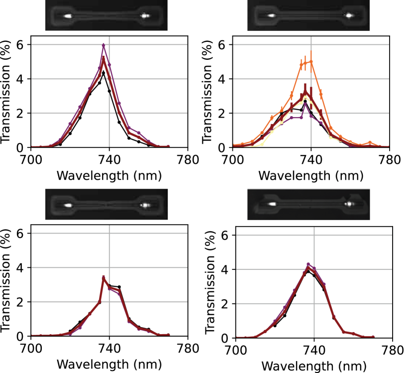
We fabricated four control devices for calibrating grating coupler efficiency on the TFLN sample. Two of these consist of TFLN tapered waveguides connected at the tips and two are constant-width waveguides. Transmission statistics were taken multiple times over 2 months for all four control devices as well as the heterogeneously integrated device. Transmission values are relatively consistent across multiple measurements, with any variance attributed to alignment or thermal fluctation, as well as gradual condensation in the cryosystem. Because the TFLN tapered waveguides introduce uncharacterized scattering, we only use the fully-connected constant-width waveguides for “control device” measurements. For measurements performed in the main text, we use connected device “2” as the control device. Connected device “4” was damaged during measurements and could not be used to calibrate transmission measurements. By measuring both devices, “2” and “4”, we can estimate the total grating coupler in-to-out-coupling transmission at nm to range between and , and averaging to (we assume negligible loss in the waveguide). This is pictured in Fig. 7. These values reasonably match the simulated in-to-out-coupling efficiencies of the grating couplers simulated via FDTD in section 12.
From these transmission measurements, we determine the taper efficiency of a second fully-integrated device (different from that presented in the main text) to be per taper facet at nm, demonstrating the repeatability of our pick and place transfer procedure. These measurements are illustrated in Fig. 8.
6 Emitter-Nanobeam Coupling Simulations
To verify the validity of our confocal versus coupler collection channel count rates, we use Lumerical FDTD to perform simulated sweeps of dipole emitter orientation and position while monitoring transmission through the different collection channels. We simulate a nanobeam with nm width and nm thickness, modeling the single mode region of our tapered diamond devices. We place a monitor at the end of each nanobeam to observe transmission coupled into the TFLN waveguide, and a monitor directly above the emitter to collect out-of-plane, confocal scattering.
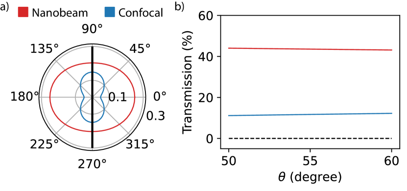
To investigate the effects of dipole orientation, we sweep the polar angle, , of the dipole from °to °to account for slight crystalline misalignment out of plane. We sweep the azimuthal angle, , between °and °, accounting for misalignment stemming from both the cut of the bulk crystal and lithography. For cut diamond with devices perfectly aligned to the cubic axes, we expect both and to be °, given diamond’s tetrahedral structure. Taking slices at both °and °and summing the transmitted power at both ends of the nanobeam, we see that in-nanobeam transmission (coupler channels) is greater than out-of-plane confocal collection, as shown in Fig. 9.
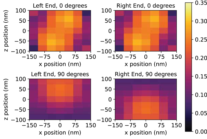
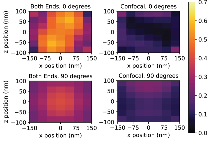
For sweeps of dipole position in the nanobeam cross-section, we maintain °. We vary between °and °only, given these two angles correspond to maximum and minimum contrast between confocal and integrated transmission. Again, we observe that integrated collection channels consistently perform equally to or outperform the out-of-plane collection consistently across all emitter positions by nearly 5-fold Fig.11. We stress that because of realistic losses from optics and the angular dependence of the collection objective, we see instead an increased 10-fold improvement in experimental device demonstration.
7 Grating Coupler Simulations
In Fig.12, we demonstrate simulated design parameters for our grating couplers. Our couplers are approximately 2 m wide and 10 m long with a designed pitch in CAD of nm. The duty cycle is swept to improve coupling bandwidth. In practice, our actual devices and grating pitch differ a bit due to fabrication discrepancies from CAD. For these parameters, we simulate an expected out-coupling efficiency from a single-mode source in the waveguide of approximately 51.7%, depicted in Fig.12(a). In-coupling of the light is more difficult, due to the multimoded behavior of the TFLN waveguide at 737 nm. Fig. 12(b) displays a map of the simulated in-coupling efficiency into the waveguide fundamental mode as a function of the incident beam placement and focal plane. For the source placement corresponding to the maximum transmission from free space into the waveguide, we simulate an expected transmission into the fundamental waveguide mode of approximately . Multiplying the single-mode input and output efficiencies together indicates that we can expect a single-mode in-to-out coupling through the simulated control device of approximately , similar to our demonstrated experimental coupling. The full multimode transmission is expected to be slightly greater, and we expect these numeric results to upper-bound our experimentally measured grating efficiencies.
8 Power-Dependent Autocorrelation
Each autocorrelation measurement presented in the main text is extracted from a series of power-dependent measurements. The full series of measurements are provided here, demonstrating how for both collection schemes, does not fall below , the single emitter threshold, but still demonstrates predominantly single emitter behavior of the interrogated spot.
9 Focus-Dependent PL
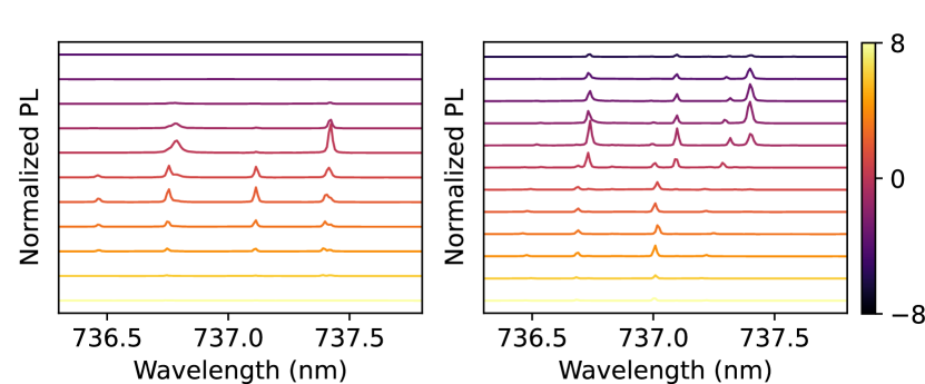
We compare the integrated device’s emission into a confocal collection channel to emission into the TFLN waveguide channel by varying the confocal excitation and collection foci and recording the resulting photoluminescence (PL) spectra measured via each collection channel.
For the confocal excitation and collection scheme (C/C configuration), we step the foci in tandem, while localized to the same coordinate and plot the results in Fig. 14(a). While we observe emerging transitions at different foci, they mostly overlap in the C/C collection, maintaining the appearance of a “single” emitter at multiple focal planes. We predominantly observe a decrease in collected light as the device is moved out of focus.
We repeat this measurement for the confocal excitation with the C/CP configuration. In this configuration, only the confocal excitation plane is stepped, while the collection plane is fixed on the TFLN grating couplers. We plot the results in Fig. 14(b). Here, we more clearly observe multiple emitter transitions appearing at different foci, including a number not captured at all through confocal channels.
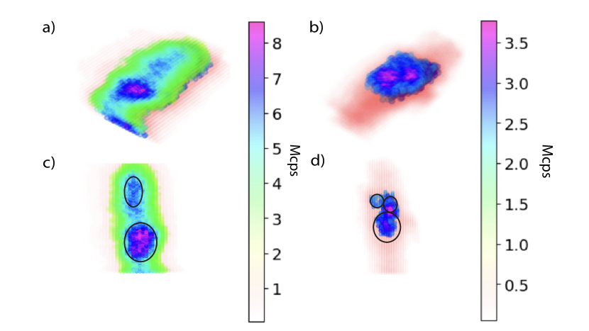
We also collect full PL maps in the X-Y plane at each interrogated focal plane. For each collection configuration, we overlay this data, with the axis corresponding to focal plane shifts, thereby generating a 3D map of suspected emitter locations. The results, shown in Fig. 15, further accentuate the differences between the two collection configurations. First, by comparing Fig. 15(a) and Fig. 15(b), we observe greater background signal and increased blurring of predicted emitter locations in the C/C configuration (Fig. 15(c)). However, in the C/CP configuration, we more clearly identify what we believe to be small clusters of emitters (Figure 15(d)). Overall, the data suggests that the TFLN waveguide collection channels are less sensitive to background fluorescence as compared to the confocal collection channels. This difference might be useful in future studies for resolving emitters in 3D space. However, the waveguide collection channels may be more susceptible to collecting in-nanobeam scattering and coupling to un-targeted emitters. Furthermore, our collection here must be calibrated to the in/out-coupling of the gratings, as described in sections 4 and 7.