Spatially resolved dielectric loss at the Si/SiO2 interface
Abstract
The Si/SiO2 interface is populated by isolated trap states which modify its electronic properties. These traps are of critical interest for the development of semiconductor-based quantum sensors and computers, as well as nanoelectronic devices. Here, we study the electric susceptibility of the Si/SiO2 interface with spatial resolution using frequency-modulated atomic force microscopy to measure a patterned dopant delta-layer buried beneath the silicon native oxide interface. We show that surface charge organization timescales, which range from , increase significantly around interfacial states. We conclude that dielectric loss under time-varying gate biases at and sub- frequencies in metal-insulator-semiconductor capacitor device architectures is highly spatially heterogeneous over length scales.
Semiconductors are emerging as a promising platform for spin-based quantum sensing and computation, with a clear path to scalability and long coherence times. In one widely adopted architecture, single dopant atoms are buried some nanometers beneath the semiconductor surface, where they are electronically accessed by means of an applied gate voltage[1, 2, 3, 4]. Silicon is a promising host lattice, in large part because existing Si microfabrication technologies, which have been refined over the past 50 years, are unparalleled for any other material[2, 4]. Despite these engineering accomplishments, however, it is impossible to fabricate a Si surface which is entirely homogeneous. In particular, if the surface has a SiO2 overlayer, a variety of defects such as and centres[5] populate the Si surface. These states modify the electronic environment near the surface resulting in, for example, random telegraph fluctuations (1/f noise)[6, 7] or threshold voltage shifts[8].
The stability and robustness of buried semiconductor qubits depends on the dielectric dispersion of the native lattice (i.e. electronic bath)[9]. In particular, as semiconductor quantum devices increase in scale (that is, as the number of qubits increases) it is becoming increasingly important to understand inhomogeneities of the susceptibility of the Si surface[10]. The lateral spacing of buried spin qubits is on the order of nanometers[1, 4], so dielectric dispersion must be measured at this scale. Classical computation is also not immune to defect states at the Si surface; indeed, as circuit components shrink to nanometer dimensions, surface effects play an increasingly dominant role in device function[11]. It is thus important to understand the origin of inhomogeneity in the electronic properties of nanoscale devices.
In this work, we measure the spatial inhomogeneity of dielectric dispersion at a Si/SiO2 interface with nanometer spatial resolution using frequency-modulated atomic force microscopy (fm-AFM)[12, 13]. The sample studied here is a patterned n-type Si surface that is terminated with of native oxide. Figure 1 shows the spatial variability of dielectric loss measured near two different Si/SiO2 trap sites observed in this surface, at variable tip-substrate gate bias . The dielectric dispersion is bias-dependent and highly sensitive to spatially localized interfacial states. We find that the relaxation times at the Si surface range between , where there is a significant increase in this timescale around isolated trap states. The measurement methodology will now be briefly discussed, before being applied to study the sample described above.
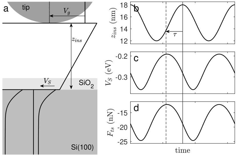
At large () tip-sample separations in non-magnetic systems, where the tip-sample force is predominantly electrostatic, the fm-AFM tip-sample junction can be described as a metal-insulator-semiconductor (MIS) capacitor[14, 15, 16, 17, 18, 19, 20]. In this work, the MIS capacitor is comprised of a metallic tip, an insulating vacuum gap of thickness (composed of the tip-sample vacuum gap plus a layer of SiO2), and an n-type Si(100) substrate, as illustrated in Figure 2a. The total capacitance of this system () is made up of the insulator (oxide and vacuum, ) and interfacial () capacitances in series:
| (1) |
where describes the space-charge organization (i.e. band bending) at the silicon-oxide interface. For the low-frequency MIS capacitor, loss occurs because each capacitance has a non-zero charging / discharging timescale . Assuming that there are no mobile carries in the oxide, is limited by the charging and discharging characteristics of (i.e. is the time required to establish a surface potential , which is non-zero due to finite carrier mobility). In other words, corresponds to the Debye relaxation timescale of the interfacial capacitor.
fm-AFM is a dynamic microscopy, which is why it can be used to characterize dielectric dispersion[21, 22, 23, 24, 25]. In fm-AFM, a cantilever-mounted tip is driven using a self-oscillation loop on the cantilever resonance at a constant oscillation amplitude above a sample surface. This means that over every oscillation cycle, the insulator thickness varies in time, as is shown in Figure 2b. Consequently, the surface charge organization (i.e. , band bending) varies in time (Figure 2c). The tip-sample force , which is related to the semiconductor surface charge density[26], therefore also varies in time (Figure 2d). leads to a shift in with respect to the free natural resonance . Assuming harmonic oscillation where , the frequency shift and drive amplitude are[27, 28, 25]:
| (2a) | |||
| (2b) | |||
where and are the spring constant and Q-factor of the cantilever. Equation 2 shows that is related to the components of which are in-phase with , and depends on the out-of-phase components. Therefore, a non-zero surface charge organization timescale manifests as in increase in [14]. By fitting measurements to modelled (given Equation 2b, where is the time-dependent force between the plates of a one-dimensional MIS capacitor[29]), the best-fit can be determined.
If is small with respect to the cantilever oscillation period, the system can be approximated as having a delta function response at :
| (3a) | ||||
| (3b) | ||||
| (3c) | ||||
where is the interfacial polarization (i.e. band bending), is the time-dependent low-frequency susceptibility ()[11], and is the electric field at the surface. In the quasi-static limit, and are known from the MIS capacitor model, so once the best-fit is known, the experimental (and ) can be determined. If is nonzero, the Fourier transform of given in Equation 3 is complex, and can be used to determine the loss tangent () according to:
| (4) |
where is the frequency-dependent permittivity. is the sum of high-frequency losses ( due to atomic and electronic polarizations (i.e. bound charges) and low-frequency losses due to finite sample conductivity (i.e. free carriers)[30, 31, 32]:
| (5) |
The results shown in this work were measured in the low-frequency regime () where free carriers dominate loss, such that . An increase in , therefore, indicates an increase in the equivalent series resistance of , meaning that more energy is dissipated by Ohmic loss[21, 33].
I Results
The sample measured in this work contains patterned squares of variable two-dimensional dopant density, up to a maximum of [34], on a background substrate doping of . The un-patterned background is bulk doped with phosphorous, while the patterned squares are delta-doped with arsenic with a dopant layer thickness of approximately . The entire wafer is capped by of epitaxial Si, the surface of which has subsequently formed of native SiO2, as determined by secondary mass ion spectroscopy[34]. The results shown in Figures 1 and 3 were measured in the background (lowest dopant density) region.
Spatial inhomogeneity – The Si/SiO2 interface is prone to trap states which modify the electronic properties of the MIS capacitor[6, 35, 29]. In particular, interfacial traps (such as Pb0 and Pb1 centers) which have energy levels within the band gap interact significantly with the Si surface charge[35, 36]. Donor-like traps (e.g. Figure 1a-c), which have energies in the lower half of the band gap, can become positively charged via emission of an electron to the valence band. Acceptor-like traps (e.g. Figure 1d-f), which have energies in the upper half of the band gap, can become negatively charged via capture of an electron from the conduction band[29, 36]. The interface state energies are fixed with respect to the band edges[6]. This means that the interface state occupancy depends on (and therefore, ), since capture or emission into a trap state depends on its energy with respect to the Fermi level .
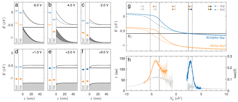
Figure 3(a-f) shows band diagrams at various biases at the bottom (maximum , solid lines) and top (minimum , dashed lines) of the cantilever oscillation. Two trap state energies, corresponding to a donor-like trap (orange) and an acceptor-like trap (blue), are shown at the bottom and top of the cantilever oscillation. An empty circle indicates an unoccupied state, and a filled circle an occupied state. The donor-like trap is unoccupied at high negative voltage, but as decreases and the bands flatten and bend downward, the donor trap energy lowers below , and it becomes occupied. The acceptor-like trap is unoccupied from negative biases up to positive biases in the accumulation regime, where the trap energy lowers below and it becomes occupied. The trap state energies found here ( above the valence band for the donor-like trap and above the valence band for the acceptor-like trap) are in agreement with accepted levels for states[37, 38].
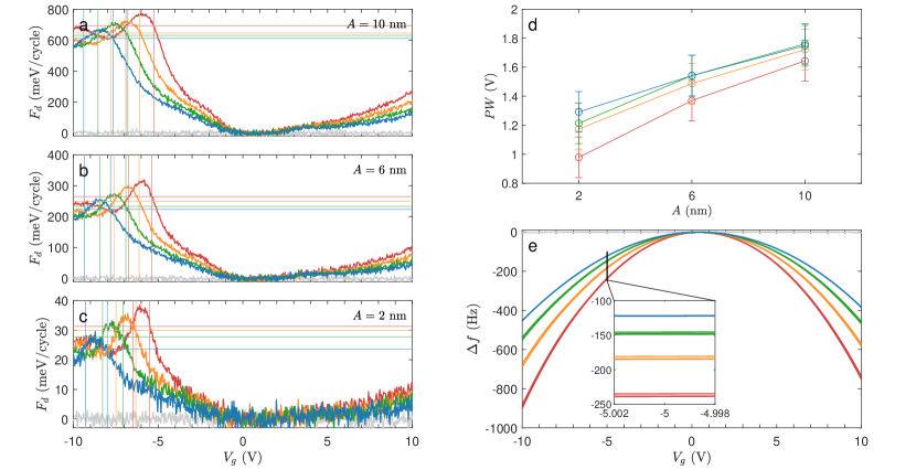
At certain biases, the trap level shifts above and below the Fermi energy during every oscillation cycle: Figure 3b shows a scenario where the donor-like trap is unoccupied at the bottom of the cantilever oscillation and occupied at the top; Figure 3e shows an acceptor-like trap which is occupied at the bottom and unoccupied at the top. The complete bias dependence of the occupation of each trap is shown in Figure 3g. The at which the state energy falls below is the crossing point, where the state occupancy switches from unoccupied to occupied. Figure 3h shows the bias-dependent above the trap states, as well as a region devoid of either type of trap (grey). At biases within the crossing points, there is a significant increase in as compared to the trap-free spectrum. Capture and re-emission out of a trap state demands a re-organization of the surface charge density, and so when this occurs over every oscillation cycle, there is an additional equilibration timescale which leads to an increase in , and therefore . The donor-like peak is wider than the acceptor-like peak because there is a larger difference in the donor-like crossing points at the top and bottom of the cantilever oscillation. Additionally, the peak width is related to the oscillation amplitude (which for a static capacitor configuration corresponds to increasing the AC gate bias amplitude): If the oscillation amplitude increases, the crossing point difference also increases, and the peak broadens. (See the Supplementary Materials.)
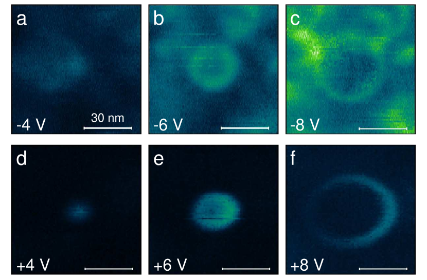
This bias-dependent spatial inhomogeneity of manifests as the ring-like features shown in Figure 1 and Figure 4[39]. Any spatially localized process which exhibits a peak in a bias spectrum in fm-AFM manifests as a ring when imaged spatially at constant height[40]. Specifically, the ring shape is due to the spatial localization of the top gate (tip), which introduces circularly symmetric equipotential lines at the sample surface. As the tip moves in , , or away from a trap state, the peak shifts to more extreme biases. The dependence of the donor-like trap bias spectrum, showing a peak shift toward negative as increases, is shown in the Supplementary Materials.
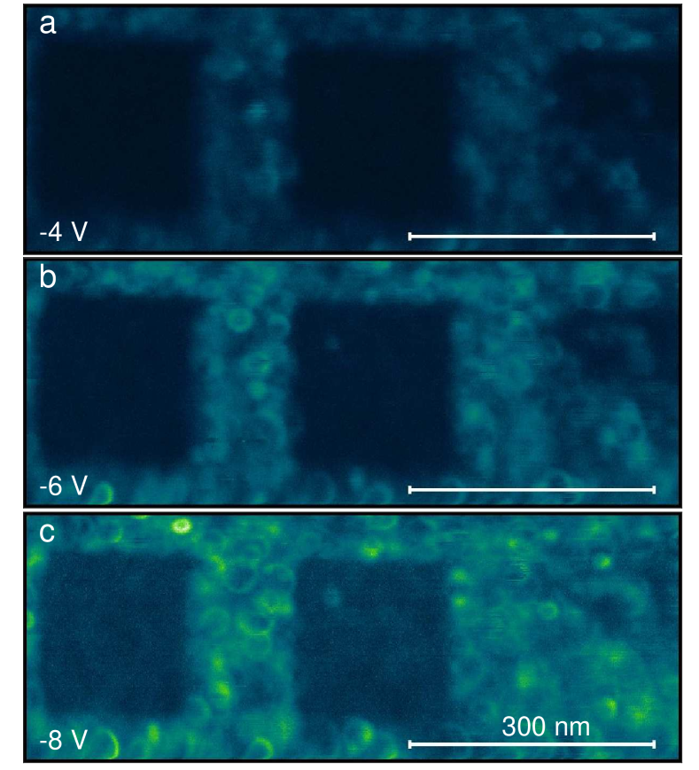
Dopant density dependence – Three “delta-doped” patterned squares of this sample can be seen in Figure 4. The two left-most squares have the highest dopant density, the right-most square has an intermediate dopant density, and the un-patterned background has the lowest dopant density. Figure 4 shows an overall trend where, as the dopant density increases, decreases. This is due to the increased Si metallicity in the patterned regions: As the dopant density increases, the resistivity decreases, meaning that the equivalent series resistance decreases, and so does .
There is additionally a dopant density dependence in the ring density. Figure 4 shows that there are many donor-like rings at negative biases in the background region, with a density on the order of . (The acceptor-like rings are much sparser: Measurements at positive bias – not shown – exhibited fewer than 5 rings over the area shown in Figure 4.) In the case of both donor-like and acceptor-like traps, the ring density decreases as dopant density increases. This can also be understood as being due to the increased metallicity of the patterned squares: Interfacial states are still expected to be present, but as the dopant density increases, band bending decreases, meaning that the effect described in Figure 3 occurs at much larger biases.
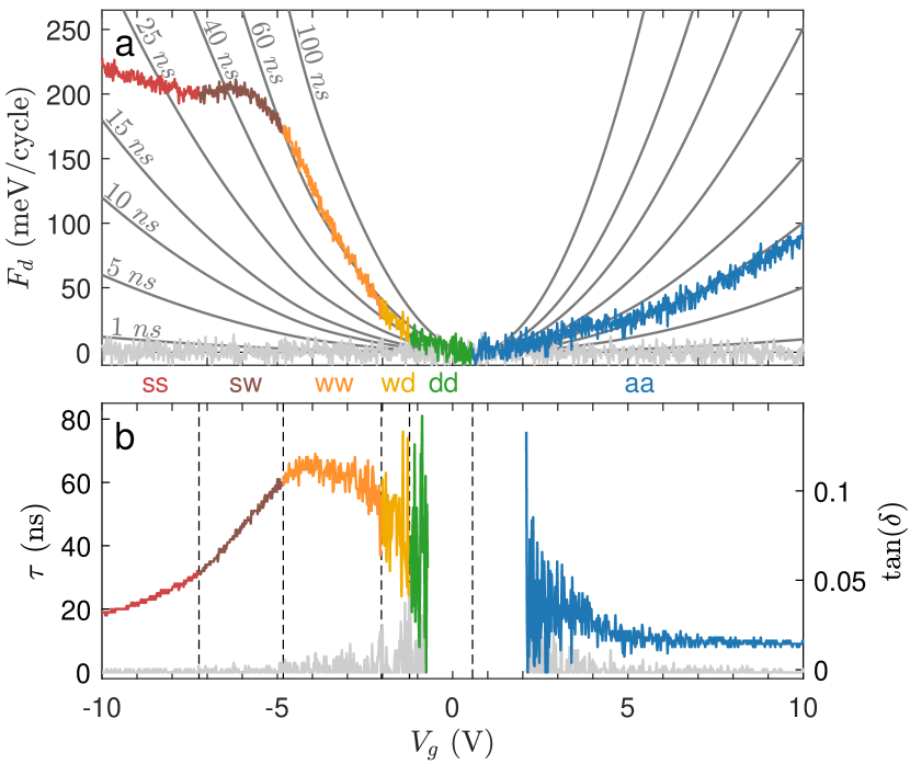
Bias dependence – The nature of the charge organization at the semiconductor surface is highly bias-dependent. This can be seen in the band diagrams in Figure 3(a-f), where is larger at negative biases than positive biases. Even in the absence of interfacial states, the surface charge density continually re-organizes (i.e. there is a change in ) over every cantilever oscillation cycle, meaning that is non-zero. The magnitude of depends on over every oscillation cycle: If is large, is large. This bias dependence might be equivalently understood in terms of the operation regimes of the MIS capacitor, which are shown in Figure 5a (where s– strong inversion; w– weak inversion; d– depletion; a– accumulation). At some biases, the capacitor switches between different charge distribution regimes over every oscillation cycle. For example, around , the capacitor is under strong inversion at the bottom of its oscillation and weak inversion at the top (i.e. the ‘sw’ regime). In the ww, wd, and dd regimes, the charge re-organization occurs predominately in the depletion region, and there is a significant change in the depletion width over every oscillation cycle. In these regimes, is large, and consequently (Figure 5b) and (Figure 5c) are maximized. In the ss and aa regimes, is approximately constant, and most of the charge re-organization occurs immediately at the semiconductor surface. In these regimes, is small, meaning that there is very little surface charge re-organization, so and decrease.
II Conclusions
We show that the magnitude of dielectric losses at the Si/SiO2 interface is highly inhomogeneous[10, 39, 20], dopant density-dependent, and gate bias-dependent. In particular, interfacial trap states lead to a dramatic increase in dielectric loss at particular biases corresponding to the trap state energy. Increasing the AC gate bias amplitude increases the width of this peak. Increasing the distance between the tip and the trap (which for a static capacitor corresponds to the system geometry or, if a qubit is acting as a noise spectrometer of the trap state[9], the distance between the qubit and the trap) leads to a peak shift toward larger voltages.
These results were measured far below the resonance frequency of the interfacial capacitance. This is necessarily the case, as the MIS capacitor model used to interpret these results is quasi-static. However, the values of that were measured range between (depending on and the proximity to a trap state), which corresponds to an interfacial capacitor resonance frequency between . This frequency range encompasses typical Rabi frequencies of buried spin qubits, which are between [41, 42]. As a result, the effective amplitude and phase of the potential at the location of a qubit will be a function of the temporal structure of the applied bias pulse sequence and the local position and energy level of defect states.
Note that the values of shown in these results are much greater than the typical values () used for spin qubit readout. The characteristics of the MIS charge organization depend on the capacitor geometry. Here, the closest tip-sample separation is is , but for the same capacitor with a insulator thickness (e.g. for a metal-oxide-semiconductor structure with a oxide thickness), the peak which occurs at in Figure 3h can be expected to occur closer to .
Finally, it can be expected that the room temperature loss tangents measured here (which are similar to values reported elsewhere[43, 32, 31, 44]) will be several orders of magnitude smaller at cryogenic temperatures[30, 45], as carrier concentrations decrease and various mobility-limiting phonon scattering mechanisms are reduced[44]. Yet, as long as the mobility is non-infinite, these bias-dependent (and trap-dependent) dielectric losses occur under any time-varying electric field, and so should be taken into consideration for the continued development of semiconductor-based quantum sensors and computers, as well as nanoelectronic devices.
III Methods
Experimental setup – All experimental results presented in this work were collected with Nanosensors platinum-iridium coated silicon tips (PPP-NCHPt) with approximately resonant frequency, spring constant , and a Q-factor of approximately . experiments were conducted at room temperature, which was assumed to be , in UHV (). The oscillation amplitude, unless otherwise stated in amplitude-dependence experiments, was . For all modelling and measurements, the bias was applied to the tip and the sample was grounded.
Bias spectroscopy specifications– Each bias spectrum includes the forward (positive to negative ) and backward curve superimposed, showing that there is negligible hysteresis with bias. Each forward and backward curve is the average of 10 individual sweeps, which took about each to acquire.
Imaging specifications– The images shown in this work were measured by multi-pass imaging. In the first pass, the tip followed the topography defined by at a setpoint frequency shift . In subsequent passes, the tip followed this same topography ( tip lifted), but was set to the displayed values, and and varied. The positions, radii, and quantity of the rings shown here were stable over the course of several weeks of measurement.
Sample fabrication – The phosphorus-doped () Si(001) substrate is thick. The delta-doped regions at variable arsenic-dopant density were fabricated using scanning tunnelling microscopy-based hydrogen resist lithography and encapsulated with a epitaxial intrinsic silicon layer plus a native oxide.
MIS model parameters – A MIS capacitor model[29] was used to study the capacitances of this system. The input parameters were: A closest tip-sample separation () of , tip radius , , electron affinity , tip work function , electron and hole effective masses and , n-type dopant density , and band gap energy . The band gap was a fit parameter, and is smaller than the expected for bulk Si. This discrepancy could be due to surface bandgap narrowing due to the presence of the large surface state density, as in [46, 47].
IV Acknowledgements
This research was supported by Natural Sciences and Engineering Research Council of Canada (NSERC) Alliance Grants – Canada-UK Quantum Technologies, an NSERC Discovery Grant, and Fonds de recherche du Québec – Nature et technologies, as well as the Engineering and Physical Sciences Research Council [grants EP/R034540/1, EP/V027700/1, and EP/W000520/1] and Innovate UK [grant 75574]. The authors would also like to thank Kirk Bevan and Hong Guo for stimulating discussions.
References
- Wellard et al. [2003] C. J. Wellard, L. C. L. Hollenberg, F. Parisoli, L. M. Kettle, H.-S. Goan, J. A. L. McIntosh, and D. N. Jamieson, Physical Review B 68, 10.1103/physrevb.68.195209 (2003).
- Morton et al. [2011] J. J. L. Morton, D. R. McCamey, M. A. Eriksson, and S. A. Lyon, Nature 479, 345 (2011).
- Zhang et al. [2018] X. Zhang, H.-O. Li, G. Cao, M. Xiao, G.-C. Guo, and G.-P. Guo, National Science Review 6, 32 (2018).
- Gonzalez-Zalba et al. [2021] M. F. Gonzalez-Zalba, S. de Franceschi, E. Charbon, T. Meunier, M. Vinet, and A. S. Dzurak, Nature Electronics 4, 872 (2021).
- Kato et al. [2006] K. Kato, T. Yamasaki, and T. Uda, Physical Review B 73, 10.1103/physrevb.73.073302 (2006).
- Kirton et al. [1989] M. J. Kirton, M. J. Uren, S. Collins, M. Schulz, A. Karmann, and K. Scheffer, Semiconductor Science and Technology 4, 1116 (1989).
- Payne et al. [2015] A. Payne, K. Ambal, C. Boehme, and C. C. Williams, Physical Review B 91, 10.1103/physrevb.91.195433 (2015).
- Campbell et al. [2007] J. P. Campbell, P. M. Lenahan, C. J. Cochrane, A. T. Krishnan, and S. Krishnan, IEEE Transactions on Device and Materials Reliability 7, 540 (2007).
- Wang and Clerk [2021] Y.-X. Wang and A. A. Clerk, Nature Communications 12, 10.1038/s41467-021-26868-7 (2021).
- Ambal et al. [2016] K. Ambal, P. Rahe, A. Payne, J. Slinkman, C. C. Williams, and C. Boehme, Scientific Reports 6, 10.1038/srep18531 (2016).
- Chen et al. [2019] S.-H. Chen, S.-W. Lian, T. R. Wu, T.-R. Chang, J.-M. Liou, D. D. Lu, K.-H. Kao, N.-Y. Chen, W.-J. Lee, and J.-H. Tsai, IEEE Transactions on Electron Devices 66, 2509 (2019).
- Albrecht et al. [1991] T. R. Albrecht, P. Grütter, D. Horne, and D. Rugar, Journal of Applied Physics 69, 668 (1991).
- García [2002] R. García, Surface Science Reports 47, 197 (2002).
- Cowie et al. [2022] M. Cowie, R. Plougmann, Z. Schumacher, and P. Grütter, Physical Review Materials 6, 10.1103/physrevmaterials.6.104002 (2022).
- Feenstra et al. [2006] R. M. Feenstra, Y. Dong, M. P. Semtsiv, and W. T. Masselink, Nanotechnology 18, 044015 (2006).
- Johnson et al. [2009] J. P. Johnson, N. Zheng, and C. C. Williams, Nanotechnology 20, 055701 (2009).
- Johnson et al. [2011] J. P. Johnson, D. W. Winslow, and C. C. Williams, Applied Physics Letters 98, 052902 (2011).
- Bernardo et al. [2022] I. D. Bernardo, J. Blyth, L. Watson, K. Xing, Y.-H. Chen, S.-Y. Chen, M. T. Edmonds, and M. S. Fuhrer, Journal of Physics: Condensed Matter 34, 174002 (2022).
- Wang and Williams [2015] R. Wang and C. C. Williams, Review of Scientific Instruments 86, 093708 (2015).
- Winslow and Williams [2011] D. Winslow and C. Williams, Journal of Applied Physics 110, 114102 (2011).
- Denk and Pohl [1991] W. Denk and D. W. Pohl, Applied Physics Letters 59, 2171 (1991).
- Eslami and Caputo [2021] B. Eslami and D. Caputo, Applied Sciences 11, 6813 (2021).
- Oyabu et al. [2006] N. Oyabu, P. Pou, Y. Sugimoto, P. Jelinek, M. Abe, S. Morita, R. Pérez, and Ó. Custance, Physical Review Letters 96, 10.1103/physrevlett.96.106101 (2006).
- Suzuki et al. [2014] K. Suzuki, K. Kobayashi, A. Labuda, K. Matsushige, and H. Yamada, Applied Physics Letters 105, 233105 (2014).
- Kantorovich and Trevethan [2004] L. N. Kantorovich and T. Trevethan, Physical Review Letters 93, 10.1103/physrevlett.93.236102 (2004).
- Hudlet et al. [1995] S. Hudlet, M. S. Jean, B. Roulet, J. Berger, and C. Guthmann, Journal of Applied Physics 77, 3308 (1995).
- Hölscher et al. [2001] H. Hölscher, B. Gotsmann, W. Allers, U. Schwarz, H. Fuchs, and R. Wiesendanger, Physical Review B 64, 10.1103/physrevb.64.075402 (2001).
- Sader et al. [2005] J. E. Sader, T. Uchihashi, M. J. Higgins, A. Farrell, Y. Nakayama, and S. P. Jarvis, Nanotechnology 16, S94 (2005).
- Simon M. Sze and Kwok K. Ng [2007] Simon M. Sze and Kwok K. Ng, Physics of semiconductor devices, Third ed. (John Wiley & Sons, Inc, 2007) Chap. , pp. 16–27,197–238.
- Checchin et al. [2022] M. Checchin, D. Frolov, A. Lunin, A. Grassellino, and A. Romanenko, Physical Review Applied 18, 10.1103/physrevapplied.18.034013 (2022).
- Krupka et al. [2006] J. Krupka, J. Breeze, A. Centeno, N. Alford, T. Claussen, and L. Jensen, IEEE Transactions on Microwave Theory and Techniques 54, 3995 (2006).
- Krupka et al. [2015] J. Krupka, P. Kamiński, R. Kozłowski, B. Surma, A. Dierlamm, and M. Kwestarz, Applied Physics Letters 107, 082105 (2015).
- Arai et al. [2018] T. Arai, D. Kura, R. Inamura, and M. Tomitori, Japanese Journal of Applied Physics 57, 08NB04 (2018).
- Stock et al. [2020] T. J. Z. Stock, O. Warschkow, P. C. Constantinou, J. Li, S. Fearn, E. Crane, E. V. S. Hofmann, A. Kölker, D. R. McKenzie, S. R. Schofield, and N. J. Curson, ACS Nano 14, 3316 (2020).
- Olof Engström [2014] Olof Engström, The MOS system (Cambridge University Press, 2014) pp. 9–128,131–167,229–260.
- Dieter K. Schroder [2009] Dieter K. Schroder, Defects in microelectronic materials and devices (CRC Press, 2009) pp. 119–158.
- Poindexter et al. [1984] E. H. Poindexter, G. J. Gerardi, M.-E. Rueckel, P. J. Caplan, N. M. Johnson, and D. K. Biegelsen, Journal of Applied Physics 56, 2844 (1984).
- Ragnarsson and Lundgren [2000] L.-Å. Ragnarsson and P. Lundgren, Journal of Applied Physics 88, 938 (2000).
- Turek et al. [2020] N. Turek, S. Godey, D. Deresmes, and T. Mélin, Physical Review B 102, 10.1103/physrevb.102.235433 (2020).
- Cockins et al. [2010] L. Cockins, Y. Miyahara, S. D. Bennett, A. A. Clerk, S. Studenikin, P. Poole, A. Sachrajda, and P. Grutter, Proceedings of the National Academy of Sciences 107, 9496 (2010).
- Huang et al. [2019] W. Huang, C. H. Yang, K. W. Chan, T. Tanttu, B. Hensen, R. C. C. Leon, M. A. Fogarty, J. C. C. Hwang, F. E. Hudson, K. M. Itoh, A. Morello, A. Laucht, and A. S. Dzurak, Nature 569, 532 (2019).
- Kawakami et al. [2014] E. Kawakami, P. Scarlino, D. R. Ward, F. R. Braakman, D. E. Savage, M. G. Lagally, M. Friesen, S. N. Coppersmith, M. A. Eriksson, and L. M. K. Vandersypen, Nature Nanotechnology 9, 666 (2014).
- Yang et al. [2006] R.-Y. Yang, C.-Y. Hung, Y.-K. Su, M.-H. Weng, and H.-W. Wu, Microwave and Optical Technology Letters 48, 1773 (2006).
- Mukherjee et al. [2016] S. Mukherjee, J. Song, and S. Vengallatore, Modelling and Simulation in Materials Science and Engineering 24, 055015 (2016).
- Liu et al. [2006] X. Liu, C. Spiel, R. Merithew, R. Pohl, B. Nelson, Q. Wang, and R. Crandall, Materials Science and Engineering: A 442, 307 (2006).
- van Vliet and Vasilopoulos [1986] C. M. van Vliet and P. Vasilopoulos, physica status solidi (a) 94, 635 (1986).
- King et al. [2010] P. D. C. King, T. D. Veal, C. F. McConville, J. Zúñiga-Pérez, V. Muñoz-Sanjosé, M. Hopkinson, E. D. L. Rienks, M. F. Jensen, and P. Hofmann, Physical Review Letters 104, 10.1103/physrevlett.104.256803 (2010).
Supplementary Materials
for
Spatially resolved dielectric loss at the Si/SiO2 interface
Megan Cowie1, Taylor J.Z. Stock2,3, Procopios C. Constantinou2, Neil Curson2,3, and Peter Grütter1
1Department of Physics, McGill University, Montréal, Québec, Canada
2London Centre for Nanotechnology, University College London, London, United Kingdom
3Department of Electronic and Electrical Engineering,
University College London, London, United Kingdom
V Peak shape dependencies
The positions of the peaks shown in Figure 3 of the main text depend on the DC bias at the trap state position. Therefore, the peak position depends on the distance between the tip (localized gate) and the interfacial trap state. When the distance is increased, the potential experienced at the trap site is reduced, and so the peak position shifts to more extreme values. This is why these peaks manifest as the rings shown in Figures 1 and 4 of the main text. Here, we show the distance dependence on the peak position, at a slight lateral displacement from an n-type ring center. Figure 6a shows bias spectra at variable tip lift () above a setpoint frequency with a oscillation amplitude . At the shortest (red), the peak occurs at ; at the largest (blue), the peak occurs at ; therefore, a increase in the distance between the trap site and the tip corresponds to a peak shift. This result agrees with the rings shown in Figure 1 in the main text, which shows that the ring radius increases by when increases by .
The peak shape also depends on the amplitude of the AC bias, and is related to the tip oscillation amplitude . Figures 6a-c show bias spectra measured at , , and . As increases, the peak width () increases. The direct correlation between and is demonstrated in Figure 6d. was found by measuring , the bias corresponding to the half-maximum value on the left side of the peak; is the bias value corresponding to this on the right side of the peak. The total peak width is their difference: . The and values are the vertical lines in Figures 6a-c; the half-maximum values are the horizontal lines. The uncertainty in is negligible on these axes. The uncertainty in is dominated by the estimation of the half-maximum on both sides of the peak. Approximating these uncertainties each as gives a peak width uncertainty of .
Figure 6e shows the bias spectra measured simultaneously with the spectra in Figures 6a-c. , which corresponds to the in-phase components of according to Equation 2a in the main text, inversely depends on : As increases, band bending at the semiconductor surface decreases, meaning that is reduced. is approximately independent of . This is demonstrated in the inset of Figure 6e, which shows that the , , and curves are essentially overlapping at each .
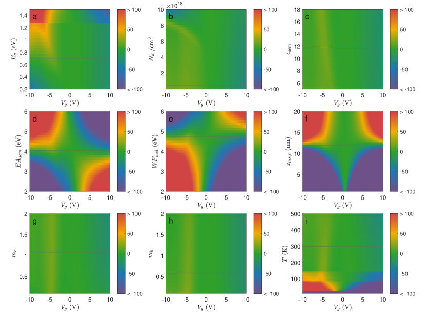
VI Model fit and parameter sensitivities
In this work, the in-phase force () and the out-of-phase force (, see Equation 2 in the main text) are analyzed to determine . First, the MIS model is fit to the spectra which, given that is small with respect to the cantilever oscillation period, is independent of within the measurement noise sensitivity. Modelled spectra at variable are then compared to the experimental results to give the best fit value. Here we demonstrate the quality of the MIS model fit and its parameter sensitivities.
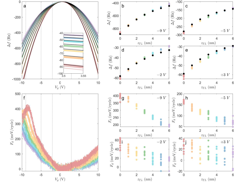
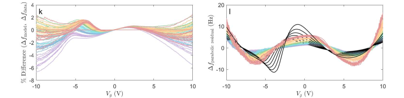
Figure 7 demonstrates the quality of the MIS model fit to the experimental bias spectra. Repeated measurements of and were performed at variable tip lift () slightly displaced from a ring center (a,f). The repeated curves overlap, which shows that the measurements are robust. and are also shown for four arbitrary biases (, , , and as a function of (b-e, g-j). The MIS model fit for variable tip lift is overlaid for the measurements (a-e), showing that there is good agreement between the model and the measurements. The residual of these curves () is also shown (k). Finally, in the MIS capacitor model, the spectrum is expected to be non-parabolic [14]. The residual of each spectrum in (a) with its parabolic fit shows this slight non-parabolicity for both the data and the model (i). There is some discrepancy between the model and the fit, which is most easily seen given the structured residual (k) and the slightly different trends in the non-parabolicity (i). Overall, however, there is good agreement, as the residual percent difference falls within .
The sensitivity of the MIS model sample parameters is demonstrated in Figure 8. The bias dependence (horizontal scale) of the residual (, colour scale) for various parameters (vertical scale) are shown. Note that the colour scale, identical for (a-i), is constrained between and . ( indicates a very large disagreement between the data and the model and indicates a very good agreement.) Since the colour scales are identical, the various parameter sensitivities can be more easily compared to one another; , for example, is a sensitive parameter whereas and are largely insensitive parameters over ‘reasonable’ values.