High Impedance Josephson Junction Resonators in the Transmission Line Geometry
Abstract
In this article we present an experimental study of microwave resonators made out of Josephson junctions. The junctions are embedded in a transmission line geometry so that they increase the inductance per length for the line. By comparing two devices with different input/output coupling strengths, we show that the coupling capacitors, however, add a significant amount to the total capacitance of the resonator. This makes the resonators with high coupling capacitance to act rather as lumped element resonators with inductance from the junctions and capacitance from the end sections. Based on a circuit analysis, we show that the input and output couplings of the resonator are limited to a maximum value of where is the resonance frequency and and are the characteristic impedances of the input/output lines and the resonator respectively.
High impedance resonators have obtained a significant attention in recent years. They have been used to obtain strong coherent coupling of microwave photons to semiconducting charge [1] and spin [2, 3, 4, 5, 6] qubits. In addition, the materials used for high impedance systems [7, 8, 9, 10, 11, 12, 13, 14] and superinductors [15, 16, 17] are also used for realizing e.g. amplifiers [18, 19] and qubits [20, 21, 22] thanks to their non-linearities. The increased coupling of the high impedance resonators arises from the added inductance giving rise to accessing the so-called ultra-strong coupling regime for electrical dipole coupled devices [23, 24], which is predicted to give rise to new fundamental physics concepts such as electroluminesence from the ground state [25]. In this letter, we investigate high impedance () resonators in a plain transmission line geometry made out of Josephson junctions. We show show how the capacitive input coupling influences on the resonator properties: a modest increase of the input coupling from MHz to MHz leads to a reduction of the resonance frequency and the characteristic impedance. Based on these findings, we determine that - despite the ultra-strong coupling to quantum structures up to GHz coupling is achievable [24] - the capacitive input coupling is limited to where is the characteristic impedance of the input lines and the resonance frequency. For our resonators, representing typical parameter values in the recently realized experiments [9, 1, 24], the largest possible capacitive coupling is limited to MHz. This imposes a trade-off between the capacitive input line coupling and the electric-dipole coupling to a quantum device: Using a low input coupling leads to suppressed resonator response visibility hampering the measurements via the resonator. The limitation can be, however, circumvented if the probing of the system is not made via the resonator input but for example via charge transport of the quantum system. In this case, the low input coupling can be compensated by using a larger drive signal amplitude. Note that the maximum bandwidth of the input line is however still limited by the trade-off. The results are thus important for designing and optimizing the high impedance resonator devices in many cases.
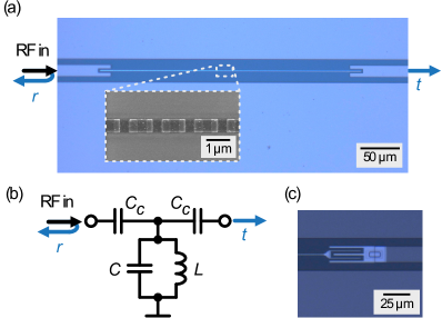
Figure 1 (a) shows the studied resonator. The RF input and output lines and the ground planes shown in light blue around the resonator are made of thick Nb film sputtered in a lift-off process on a high-resistivity intrinsic silicon wafer with a thick thermally grown silicon oxide layer. The thin Josephson junction chain between the RF lines was fabricated by a standard two-angle shadow-evaporation technique. The resist mask consisted of thick copolymer at bottom and thick polymethyl methacrylate layer on top and was patterned by e-beam lithography. First, thick Al rectangles were evaporated at an angle to the normal of the substrate followed by an in-situ oxidation for 10 minutes in 0.36 mbar of . Then, thick Al rectangles were evaporated at to connect the lower rectangles with Josephson junctions located at the overlapping areas. These Josephson junctions form a chain defining a high impedance transmission line geometry [18, 8, 9, 15, 16] where each Josephson junction yields an inductance . Here is the normal state resistance of the junction, measured from similar junctions fabricated at the same processing round as the resonator, and the superconducting gap of aluminum used as the superconductor. The junction separation of yields the inductance per unit length of . This value is more than two orders of magnitude larger than the the permeability of vacuum which sets the typical value for non-magnetic materials. The high inductance slows down the phase velocity of the signal [18] such that our transmission line with the total length of forms a /2-resonance mode in the GHz frequency band. For frequencies close to the resonator resonance frequency, this resonance mode corresponds to an equivalent LC-circuit of Fig. 1 (b) with inductance and capacitance where is the capacitance per length [26].
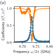
To probe the resonator properties, we couple the resonator to standard input and output lines with coupling capacitors that are identical for the input and output. Figure 2 (a) presents the measured transmission and reflection coefficient as a function of the drive frequency . A Lorentzian resonance mode at a resonance frequency of GHz is seen in the resonator response. The solid lines show fits to
| (1) |
where MHz is the internal losses of the resonator and MHz the input coupling [27]. The input coupling and the resonator frequency are connected to the circuit elements of Fig. 1 (b) as and with the total capacitance of the resonator [26, 27].
In the fits of Fig. 2 (a), the two input couplings set essentially the linewidth of the resonance and the internal losses how high the transmission coefficient increases and reflection coefficient decreases in resonance. The resonator reaches close to the ideal values and of a lossless resonator, reflecting the fact that the internal losses are significantly smaller than the couplings . Note that here the fitted value of should not be used as precise value of the internal losses but rather as a ballpark estimate of the upper limit of the internal losses. This because the value is small compared to the total linewidth and hence is prone to large uncertainties from the background transmission and reflection calibration as well as possible spurious background transmission [28]. These uncertainties are particularly large for this case since the measured response is slightly above the GHz measurement window of our setup. Continuing now with the Josephson junction parameter values and the other fitted values above, we obtain fF and fF. The characteristic impedance of the resonator is then . Note that here we use the characteristic impedance of the full circuit at the end points of the resonator. Hence this value describes the effective impedance value to which other circuit elements couple when connecting them to the typical maximal capacitive coupling point at the end of the resonator with a voltage anti-node. The characteristic impedance of the Josephson junction array, , is close to this value but naturally doesn’t depend on the coupling capacitance like does. The capacitance per unit length of the junction array pF/m matches well with similar transmission line geometries on a silicon substrate [26].
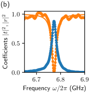
Next, we consider a resonator with larger input and output couplings. The Josephson junction chain of the resonator is kept the same and was fabricated in the same processing round as the low coupling device of Fig. 1 (a). The input and output couplings are made larger by using an inter-digitized finger geometry shown in Fig. 1 (c). The resulting response is presented in Fig. 2 (b) together with the fits yielding GHz, MHz and MHz. Again, the small value of should be taken as an indicative one for the upper limit of the internal losses. With the same inductance from the Josephson junction chain, the corresponding circuit parameter values are thus fF and fF resulting in .
When comparing the two resonator responses, we see that despite the input/output coupling is increased merely to MHz, the resonance frequency drops by GHz. This shift arises as the coupling capacitances contribute to nearly half of the total capacitance for the high coupling resonator. Correspondingly, the characteristic impedance drops by the equal amount of due to the significant added capacitance. On the other hand, the nearly unaltered internal losses and the Josephson junction chain capacitance of fF for the low coupling resonator versus fF for the high coupling resonator yield good consistency checks for our model. The extra capacitance of fF in the high coupler resonator is likely due to the increased self capacitance and extra capacitance to ground from the inter-digitized couplers. Indeed, the extra length of from the couplers corresponds to a capacitance of fF.
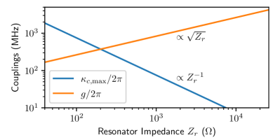
The above comparison of the two resonators yields two important points for high impedance resonator designing: 1) Even with the rather small input couplings, one needs to pay extra attention to the added total capacitance that may otherwise shift the resonance frequency uncontrollably far away from the desired value, as well as lower the resonator impedance . This is in stark contrast to the low impedance resonators where the resonance frequency shift is comparable to the coupling , see e.g. Ref. 26. 2) The significant contribution of the coupling capacitances to the total capacitance limits the highest attainable input/output coupling value . We obtain this largest coupling by taking the coupling capacitance to dominate the total capacitance, i.e. , which yields and the highest coupling as
| (2) |
In the last equality, we used the relation . For our resonators, exemplary for typical ones used in the experiments, we have MHz with and GHz. By using a single port resonator, the lowest total capacitance would be instead, and the highest possible coupling increases to . Interestingly, these kind of resonators have been shown to yield coherent coupling in the strong and ultra-strong coupling regime for interactions between the microwave photons - or more precisely plasmons [29] - in the resonator and a charge degree of freedom in a semiconducting quantum dots [24]. In these experiments, the dipole coupling value reached up to MHz with and . The largest input coupling in this device is limited then to , an order of magnitude lower than . Figure 3 summarizes the trade-off between and the dipole coupling of a semiconductor charge qubit [30] serving as an exemplary system to which the resonators couple to. Here is the capacitive coupling constant between the qubit and the resonator and the resistance quantum. We see that for , the input coupling will be significantly smaller than than , even for the more modest charge qubit couplings of the order of , typical in many experiments [31, 24, 32, 33, 34].
To recover the low impedance result connecting the frequency shift to the input coupling directly, the same characteristic impedance could be used for both the resonator and the input and output lines with . Forming the input and output lines with the Josephson junction arrays approach would be possible for our resonators without any further processing steps. However, an additional consideration would be needed for connecting the lines further to the usually used standard cabling. A "tapering" of the characteristic impedance by increasing the junction separation gradually along the line could be used. The high kinetic inductance approaches [7, 10, 11, 13] would offer also a viable option here as the characteristic impedance could be changed by widening the input and output lines gradually with the tapering. Using an inductive coupling scheme instead of the capacitive one may also provide a way to obtain couplings larger than the capacitive limit studied here.
In conclusion, we have measured the transmission and reflection coefficient response of high impedance transmission line resonators made out of Josephson junctions. By varying the capacitive input coupling, we showed that the capacitance added by the couplers has a much stronger effect on the high impedance resonators in comparison to the low impedance ones. The capacitance both reduces the resonance frequency significantly as well as reduces the impedance level. We also showed that the maximum input/output coupling is reduced and limited to , despite the dipole coupling is increased to an order of magnitude larger values for the typical resonator impedances values of the order of used in these experiments.
We thank A. Baumgartner, A. Pally, P. Scarlino, C. Schönenberger, C. Thelander and J. Ungerer for fruitful discussions, and Swedish Research Council (Dnr 2019-04111), the Foundational Questions Institute, a donor advised fund of Silicon Valley Community Foundation (grant number FQXi-IAF19-07) and NanoLund for financial support.
References
- Stockklauser et al. [2017] A. Stockklauser, P. Scarlino, J. V. Koski, S. Gasparinetti, C. K. Andersen, C. Reichl, W. Wegscheider, T. Ihn, K. Ensslin, and A. Wallraff, “Strong coupling cavity qed with gate-defined double quantum dots enabled by a high impedance resonator,” Phys. Rev. X 7, 011030 (2017).
- Landig et al. [2018] A. J. Landig, J. V. Koski, P. Scarlino, U. C. Mendes, A. Blais, C. Reichl, W. Wegscheider, A. Wallraff, K. Ensslin, and T. Ihn, “Coherent spin–photon coupling using a resonant exchange qubit,” Nature 560, 179–184 (2018).
- Mi et al. [2018] X. Mi, M. Benito, S. Putz, D. M. Zajac, J. M. Taylor, G. Burkard, and J. R. Petta, “A coherent spin–photon interface in silicon,” Nature 555, 599–603 (2018).
- Samkharadze et al. [2018] N. Samkharadze, G. Zheng, N. Kalhor, D. Brousse, A. Sammak, U. C. Mendes, A. Blais, G. Scappucci, and L. M. K. Vandersypen, “Strong spin-photon coupling in silicon,” Science 359, 1123–1127 (2018).
- Yu et al. [2023] C. X. Yu, S. Zihlmann, J. C. Abadillo-Uriel, V. P. Michal, N. Rambal, H. Niebojewski, T. Bedecarrats, M. Vinet, É. Dumur, M. Filippone, B. Bertrand, S. De Franceschi, Y.-M. Niquet, and R. Maurand, “Strong coupling between a photon and a hole spin in silicon,” Nature Nanotechnology 18, 741–746 (2023).
- Ungerer et al. [2023] J. H. Ungerer, A. Pally, A. Kononov, S. Lehmann, J. Ridderbos, C. Thelander, K. A. Dick, V. F. Maisi, P. Scarlino, A. Baumgartner, and C. Schönenberger, “Strong coupling between a microwave photon and a singlet-triplet qubit,” arXiv:2303.16825 (2023), https://doi.org/10.48550/arXiv.2303.16825.
- Barends et al. [2008] R. Barends, H. L. Hortensius, T. Zijlstra, J. J. A. Baselmans, S. J. C. Yates, J. R. Gao, and T. M. Klapwijk, “Contribution of dielectrics to frequency and noise of NbTiN superconducting resonators,” Appl. Phys. Lett. 92 (2008), 10.1063/1.2937837.
- Hutter et al. [2011] C. Hutter, E. A. Tholén, K. Stannigel, J. Lidmar, and D. B. Haviland, “Josephson junction transmission lines as tunable artificial crystals,” Phys. Rev. B 83, 014511 (2011).
- Masluk et al. [2012] N. A. Masluk, I. M. Pop, A. Kamal, Z. K. Minev, and M. H. Devoret, “Microwave characterization of Josephson junction arrays: Implementing a low loss superinductance,” Phys. Rev. Lett. 109, 137002 (2012).
- Samkharadze et al. [2016] N. Samkharadze, A. Bruno, P. Scarlino, G. Zheng, D. P. DiVincenzo, L. DiCarlo, and L. M. K. Vandersypen, “High-kinetic-inductance superconducting nanowire resonators for circuit QED in a magnetic field,” Phys. Rev. Appl. 5, 044004 (2016).
- Maleeva et al. [2018] N. Maleeva, L. Grünhaupt, T. Klein, F. Levy-Bertrand, O. Dupre, M. Calvo, F. Valenti, P. Winkel, F. Friedrich, W. Wernsdorfer, A. V. Ustinov, H. Rotzinger, A. Monfardini, M. V. Fistul, and I. M. Pop, “Circuit quantum electrodynamics of granular aluminum resonators,” Nature Comm. 9, 3889 (2018).
- Grünhaupt et al. [2019] L. Grünhaupt, M. Spiecker, D. Gusenkova, N. Maleeva, S. T. Skacel, I. Takmakov, F. Valenti, P. Winkel, H. Rotzinger, W. Wernsdorfer, A. V. Ustinov, and I. M. Pop, “Granular aluminium as a superconducting material for high-impedance quantum circuits,” Nature Materials 18, 816–819 (2019).
- Niepce, Burnett, and Bylander [2019] D. Niepce, J. Burnett, and J. Bylander, “High kinetic inductance nanowire superinductors,” Phys. Rev. Appl. 11, 044014 (2019).
- Yu et al. [2021] C. X. Yu, S. Zihlmann, G. Troncoso Fernández-Bada, J.-L. Thomassin, F. Gustavo, Ã. Dumur, and R. Maurand, “Magnetic field resilient high kinetic inductance superconducting niobium nitride coplanar waveguide resonators,” Applied Physics Letters 118, 054001 (2021).
- Bell et al. [2012] M. T. Bell, I. A. Sadovskyy, L. B. Ioffe, A. Y. Kitaev, and M. E. Gershenson, “Quantum superinductor with tunable nonlinearity,” Phys. Rev. Lett. 109, 137003 (2012).
- Altimiras et al. [2014] C. Altimiras, O. Parlavecchio, P. Joyez, D. Vion, P. Roche, D. Esteve, and F. Portier, “Dynamical Coulomb blockade of shot noise,” Phys. Rev. Lett. 112, 236803 (2014).
- Peruzzo et al. [2020] M. Peruzzo, A. Trioni, F. Hassani, M. Zemlicka, and J. M. Fink, “Surpassing the resistance quantum with a geometric superinductor,” Phys. Rev. Appl. 14, 044055 (2020).
- Castellanos-Beltran and Lehnert [2007] M. A. Castellanos-Beltran and K. W. Lehnert, “Widely tunable parametric amplifier based on a superconducting quantum interference device array resonator,” Appl. Phys. Lett. 91 (2007), 10.1063/1.2773988.
- Macklin et al. [2015] C. Macklin, K. O’Brien, D. Hover, M. E. Schwartz, V. Bolkhovsky, X. Zhang, W. D. Oliver, and I. Siddiqi, “A near quantum-limited Josephson traveling-wave parametric amplifier,” Science 350, 307–310 (2015).
- Manucharyan et al. [2009] V. E. Manucharyan, J. Koch, L. I. Glazman, and M. H. Devoret, “Fluxonium: Single Cooper-pair circuit free of charge offsets,” Science 326, 113–116 (2009).
- Hazard et al. [2019] T. M. Hazard, A. Gyenis, A. Di Paolo, A. T. Asfaw, S. A. Lyon, A. Blais, and A. A. Houck, “Nanowire superinductance fluxonium qubit,” Phys. Rev. Lett. 122, 010504 (2019).
- Pechenezhskiy et al. [2020] I. V. Pechenezhskiy, R. A. Mencia, L. B. Nguyen, Y.-H. Lin, and V. E. Manucharyan, “The superconducting quasicharge qubit,” Nature 585, 368–371 (2020).
- Frisk Kockum et al. [2019] A. Frisk Kockum, A. Miranowicz, S. De Liberato, S. Savasta, and F. Nori, “Ultrastrong coupling between light and matter,” Nature Rev. Phys. 1, 19–40 (2019).
- Scarlino et al. [2022] P. Scarlino, J. H. Ungerer, D. J. van Woerkom, M. Mancini, P. Stano, C. Müller, A. J. Landig, J. V. Koski, C. Reichl, W. Wegscheider, T. Ihn, K. Ensslin, and A. Wallraff, “In situ tuning of the electric-dipole strength of a double-dot charge qubit: Charge-noise protection and ultrastrong coupling,” Phys. Rev. X 12, 031004 (2022).
- Cirio et al. [2016] M. Cirio, S. De Liberato, N. Lambert, and F. Nori, “Ground state electroluminescence,” Phys. Rev. Lett. 116, 113601 (2016).
- Göppl et al. [2008] M. Göppl, A. Fragner, M. Baur, R. Bianchetti, S. Filipp, J. M. Fink, P. J. Leek, G. Puebla, L. Steffen, and A. Wallraff, “Coplanar waveguide resonators for circuit quantum electrodynamics,” J. Appl. Phys. 104, 113904 (2008).
- Havir et al. [2023] H. Havir, S. Haldar, K. W., S. Lehmann, K. A. Dick, C. Thelander, P. Samuelsson, and V. F. Maisi, “Quantum dot source-drain transport response at microwave frequencies,” arXiv:2303.13048 (2023), https://doi.org/10.48550/arXiv.2303.13048.
- Rieger et al. [2023] D. Rieger, S. Günzler, M. Spiecker, A. Nambisan, W. Wernsdorfer, and I. Pop, “Fano interference in microwave resonator measurements,” Phys. Rev. Appl. 20, 014059 (2023).
- Mooij and Schön [1985] J. E. Mooij and G. Schön, “Propagating plasma mode in thin superconducting filaments,” Phys. Rev. Lett. 55, 114–117 (1985).
- Childress, Sørensen, and Lukin [2004] L. Childress, A. Sørensen, and M. D. Lukin, “Mesoscopic cavity quantum electrodynamics with quantum dots,” Phys. Rev. A 69, 042302 (2004).
- Frey et al. [2012] T. Frey, P. J. Leek, M. Beck, A. Blais, T. Ihn, K. Ensslin, and A. Wallraff, “Dipole coupling of a double quantum dot to a microwave resonator,” Phys. Rev. Lett. 108, 046807 (2012).
- Mi et al. [2017] X. Mi, J. V. Cady, D. M. Zajac, P. W. Deelman, and J. R. Petta, “Strong coupling of a single electron in silicon to a microwave photon,” Science 355, 156–158 (2017).
- Khan et al. [2021] W. Khan, P. P. Potts, S. Lehmann, C. Thelander, K. A. Dick, P. Samuelsson, and V. F. Maisi, “Efficient and continuous microwave photoconversion in hybrid cavity-semiconductor nanowire double quantum dot diodes,” Nature Communications 12, 5130 (2021).
- Haldar et al. [2023] S. Haldar, H. Havir, W. Khan, S. Lehmann, C. Thelander, K. A. Dick, and V. F. Maisi, “Energetics of microwaves probed by double quantum dot absorption,” Phys. Rev. Lett. 130, 087003 (2023).