Version v6d (accepted manuscript)
Surface Direct Conversion of 511 keV Gamma Rays in Large-Area Laminated
Multichannel-Plate Electron Multipliers
Kepler Domurat-Sousa, Cameron Poe, Henry J. Frisch
Enrico Fermi Institute, University of Chicago
Bernhard W. Adams
Quantum Optics Applied Research
Camden Ertley
SouthWest Research Institute
Neal Sullivan
Angstrom Research, Inc
Published in Nuclear Instruments and Methods, Section A
Abstract
We have used the TOPAS simulation framework to model the direct conversion of 511 keV gamma rays to electrons in a micro-channel plate (MCP) constructed from thin laminae of a heavy-metal-loaded dielectric such as lead-glass, patterned with micro-channels (LMCP). The laminae serve as the converter of the gamma ray to a primary electron within a depth from a channel-forming surface such that the electron penetrates the channel surface (‘surface direct conversion’). The channels are coated with a secondary-emitting material to produce electron multiplication in the channels. The laminae are stacked on edge with the channels running from the top of the resulting ‘slab’ to the bottom; after assembly the slab is metalized top and bottom to form the finished LMCP.
The shape of the perimeter of a lamina determines the dimensions of the slab at the lamina location in the slab, allowing non-uniform cross-sections in slab thickness, width, and length. The slab also can be non-planar, allowing curved surfaces in both lateral dimensions. The laminar construction allows incorporating structural elements in the LMCP for modular assembly in large-area arrays.
The channels can be patterned on the laminae surfaces with internal shapes and structure, texture, and coatings optimized for specific applications and performance. The channels can be non-uniform across the LMCP and need not be parallel in either transverse direction.
Surface direct conversion of the gamma ray to an electron eliminates the common two-step conversion of the gamma ray into an optical photon in a scintillator followed by the conversion of the photon into an electron in a photodetector. The simulations predict an efficiency for conversion of 511 keV gamma rays of 30% for a 2.54 cm-thick lead-glass LMCP. The elimination of the photocathode allows assembly at atmospheric pressure.
1 Introduction
The ability to detect low-energy gamma rays with sub-mm space resolution in three dimensions and time resolutions less than 100 ps would open opportunities for simpler, more-capable detectors in medical imaging, particle physics, nuclear physics, astrophysics, and other fields. Low-energy gamma rays are now typically detected by the two-step conversion of the gamma ray to optical photons in a scintillating medium followed by photon conversion to electrical pulses in a photodetector [1, 2, 3, 4, 5].
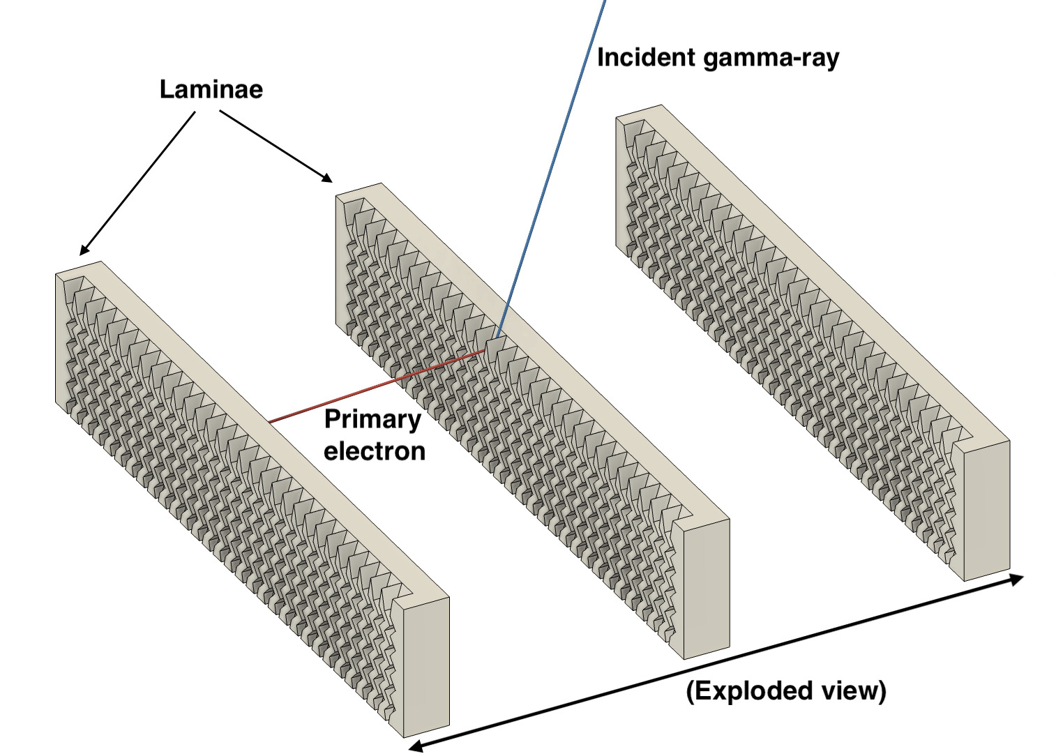
To explore alternatives at the level of the underlying physics processes, we have modeled the direct conversion of 511 keV gamma rays to electrons in a laminar micro-channel plate (LMCP) constructed from thin heavy-metal-loaded dielectric laminae such as lead-glass. The laminae serve as the converter of the gamma ray to a primary electron within a depth from a channel-forming surface such that the electron penetrates the interior channel surface (‘surface direct conversion’, or ‘SDC’). The channels are coated with resistive and secondary-emitting (SEY) material [6] to produce electron multiplication in the channel much as in a conventional MCP [7]. A 3D visualization of an LMCP is depicted in Figure 1.
The laminar design with stacked patterned laminae allows wide flexibility in the 3D shape of the LMCP, and the shapes and functionalization of the channels. Additionally, the absence of a photocathode allows modular pre-assembly of large-area arrays of LMCPs at atmospheric pressure. Minor modifications to the perimeters of the laminae can provide precision alignment and internal support against atmospheric pressure in large-area arrays in a single hermetic vessel.
This paper focuses on the surface direct conversion of 511 keV gamma rays. However, the laminar construction can be applied to a wide variety of MCP applications, from conventional uniform rectangular MCPs to non-rectangular and non-planar assemblies, with locally optimized non-uniform channel shape, size, direction, coatings, and metalizations. Substrates can be as in conventional MCPs, or appropriately optimized for charged particles, neutrons, or high-energy particle showers in a given energy range.
The organization of the paper is as follows. Section 2 is a description of the construction of the laminar MCP. Section 3 gives an overview of the lamina, including the substrate material, shape, orientation, and use as a structural element. Section 4 presents the patterned microchannels on the lamina surfaces, including methods of patterning, channel shapes, and coating methods. Section 5 describes the assembly of the laminae into a ‘slab’, which when metalized top-and-bottom becomes the LMCP. Possible slab geometries include planar and non-planar slabs, slabs non-uniform in thickness, width, or length, and slabs with non-parallel channels. Section 6 presents the results of a TOPAS Geant4-based simulation of surface direct production of electrons from 511-keV gamma rays in tungsten and a heavy-metal-loaded glass.
2 Construction of the Laminar MCP (LMCP)
The laminated microchannel plate (LMCP) is formed by assembling thin laminae, rather than the conventional method of assembling and drawing fibers [7]. An LMCP channel plate is assembled from laminae with one or both sides patterned with channels that extend from one edge of the lamina (corresponding to the top surface of the LMCP) to the other edge (the LMCP bottom). The channels can be patterned in both transverse and longitudinal directions. Options include entrance funnels, patterns of strike surfaces, and an exit ‘choke,’ such as seen in Figure 1.
If the substrate is not intrinsically resistive, the laminae can first be functionalized on both sides with a resistive layer. A secondary-emitting layer is then applied. Subsequent metalization before assembly can provide customized dynode structures in the channels.
After patterning and functionalization, the laminae are stacked, much like books on a book-shelf, and formed into the plate, here called a ‘slab’ to distinguish it from a fully-finished LMCP. The slab can vary in any of the three dimensions and be non-planar; the channels need only connect the top and the bottom, but can vary in density, size, channel-defining surfaces, functionalization, and direction within a single slab.
To form the finished LMCP, the top and bottom surfaces of the slab are appropriately metalized to supply voltage and current for electron amplification in the channels.
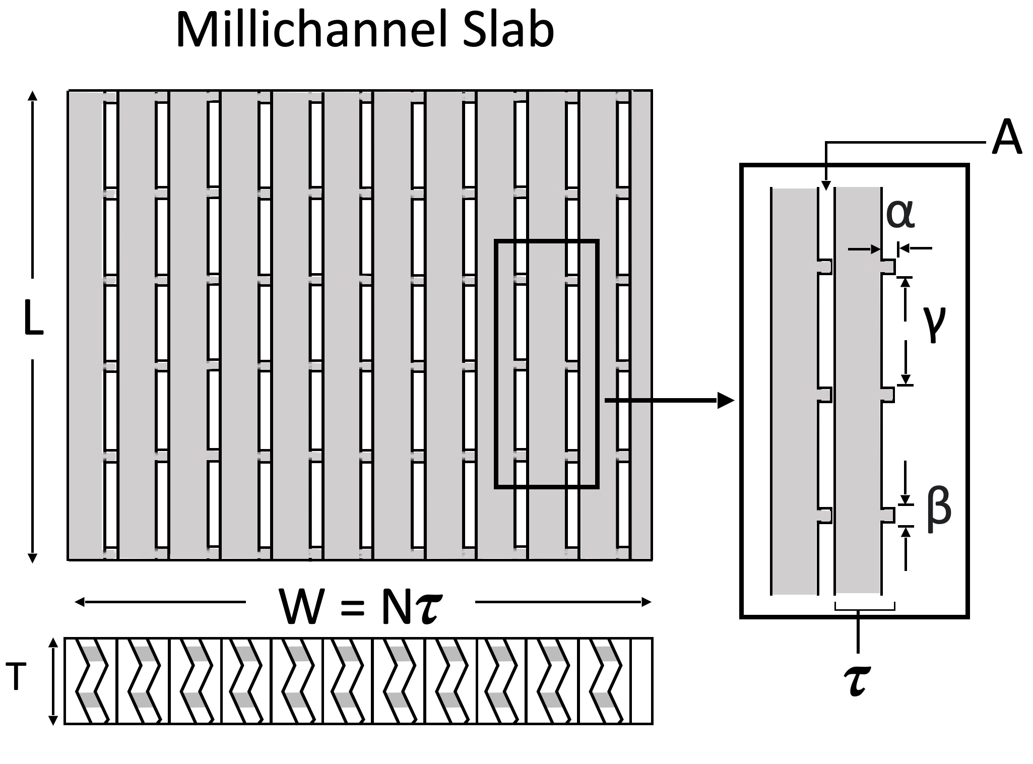
Figure 2 shows a functional diagram of a lead-glass slab with dimensions appropriate for gamma ray conversion to electrons. Both sides of the laminae are functionalized with resistive and SEY layers. The values of the channel-defining dimensions and should be comparable to the range of the primary electron from the gamma ray, e.g. 150 microns in lead-glass.
The slab outer dimensions and the shape are free to be determined by operational considerations such as the function, desired packing fraction of modules in arrays, mechanical assembly, or electrical connections. In addition to thicker slabs, multiple LMCPs, with or without an associated anode, can be stacked in series to increase the detection efficiency.
3 The Lamina Substrate
In addition to supporting the patterned channels, the lamina substrate performs three functions: (1) providing the target material for the production and escape of a primary electron from a gamma ray conversion; (2) determining the cross-sectional shape of the slab at the location of the lamina in the slab assembly; and (3) providing mechanical support and alignment mechanisms for the internal stack.
The individual shapes of the laminae determine the local cross-section of the slab. For a planar LMCP, as is typical in current commercial MCPs, the lamina are rectangular and identical. For a curved LMCP, one or more of the lamina edges will be curved. The dimensions of the laminae do not need to be the same throughout the stack; the lateral dimensions and the width of the LMCP can be varied throughout the slab. Following the analogy of the laminae stack corresponding to books on a bookshelf, the laminae may be tilted to one side, as so often happens when a bookshelf is not full.
The ability to independently shape each lamina allows incorporating the laminae as structural elements in the mechanical package. The edges of selected laminae can be shaped with protruding ‘tabs’ such that when the laminae are incorporated on edge into the slab the tabs form spacers. The spacers separate components inside the assembled detector, for example between one LMCP and another, or between the top of the top LMCP and a window or top plate of the hermetic package. The tabs on successive slabs can form a column between the top and bottom plates to support atmospheric pressure over large areas. Other features on the lamina edges can provide mechanical mounting and/or aligning mechanisms, and can also be conducting or resistive to be part of the LMCP internal electrical circuit.
Special laminae made of a non-conducting material chosen for strength, such as alumina, can be included in the slab at intervals. These ‘strong-backs’ can be structural elements in the internal mechanical assembly to support atmospheric pressure, for example.
4 Micro-Channels on the Lamina Surfaces
The laminae can be laid out flat for patterning, functionalization, and metalization of the channels prior to assembly. The laminae can be micro-patterned by many conventional methods, including additive/subtractive processes such as 3D printing. The cross-section, surface texture, and dimensions can change along the channel.
Access to the full channel surface before assembly allows customizing the interior of the channels for parameters such as gain, time resolution, pulse uniformity, and rate capability. There are many options for secondary coatings, including an option of successive coatings with selective masking. Metalization also be patterned along the channel to produce, for example, custom-spaced dynode structures and end-spoiling.
Figure 3 shows a simple regular rectilinear pattern of channels printed on a lamina that forms channels from the top of the slab to the bottom. The channels can be patterned with a bias angle such that two superposed slabs form a chevron.
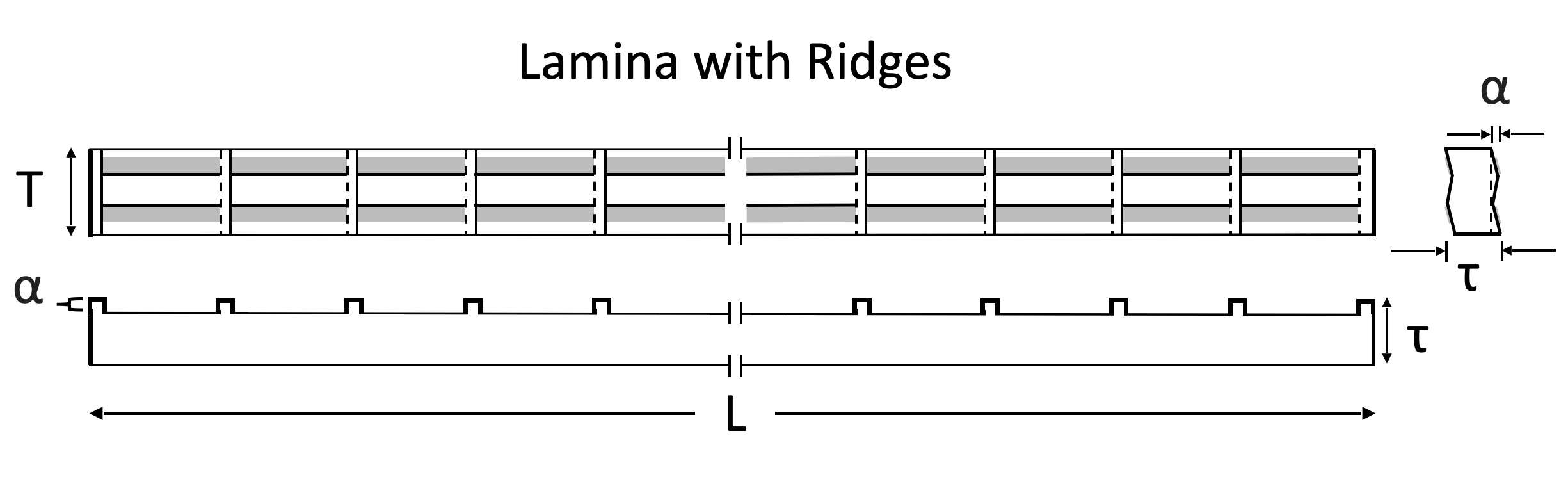
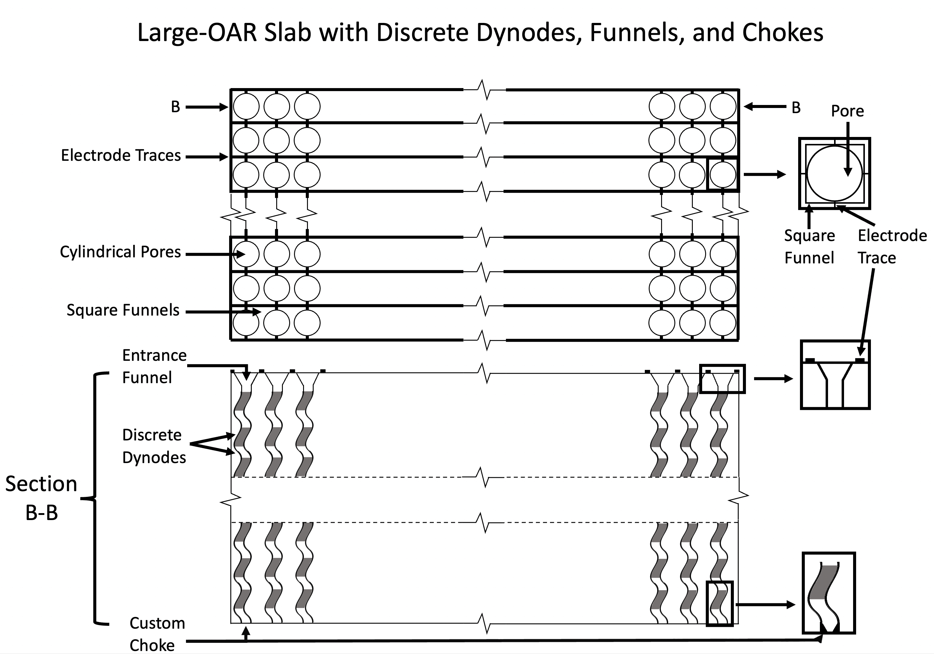
Figure 4 shows a slab composed of laminae with an example pattern based on cylindrical channels with an entrance funnel, discrete metalized dynodes, a mild exit ‘choke’, and exit end-spoiling. The square entrance funnels cover the entrance surface except for the interwoven metalized traces that supply the voltage and current to each channel, resulting in a large open-area ratio.
5 Assembling the Laminae
After functionalization, the laminae are bonded together into a solid slab. The laminar construction allows forming non-uniform and non-planar slabs. The laminae can be non-rectangular to form a desired shape transverse to the stacking direction. The laminar construction also allows making slabs of non-uniform thickness by changing the dimensions of the laminae during the assembly of the stack. Precision locating holes or external reference grooves can be used to enforce precision mating of the two channel patterns on neighboring laminae. In addition to this flexibility in shape and thickness of the slab, laminar construction enables non-parallel channels and/or channels of varying dimensions, as may be desirable from local rate considerations or for directing the exit shower.
Once the laminae have been bonded together into a slab, the top and bottom surface of the slab can be metalized to provide the electrodes to supply voltage across the channels and current through the surface of the channels. The thin traces between the funnels in the plan view of Figure 4 are an example top electrode.
6 Simulation using the TOPAS Geant4-based Package
In order to test the viability of such laminar MCP geometries, we have modified [8] the TOPAS package [9] to study their efficiencies. Special attention has been paid to the efficiency of direct conversion of 511-keV gamma rays via surface direct conversion in laminae containing high-atomic number nuclei such as lead (Pb) or tungsten (W) for Time-of-Flight Positron-Emission Tomography (TOF-PET).
6.1 Direct Gamma Conversion to Electrons: Compton Scattering and the Photoelectric Effect
The three fundamental processes for conversion of a gamma ray to charged particles are the Photoelectric Effect, Compton Scattering, and, at gamma ray energies above 1 MeV, Pair Production. The capability to convert a sub-MeV gamma ray directly into an electron, which is then multiplied in the LMCP, has the disadvantage that the efficiency is inherently low per unit length of material.
The efficiency for a gamma ray to create an electron cascade in a channel for a given material is determined by two factors. First, the cross sections and energy distributions for producing a ‘primary’ electron depend on the substrate. Second, the range of sub-MeV electrons in heavy materials is short; only conversions close to the functionalized channel interior surface reach it before ranging out. These production and escape factors vary with material: tungsten (W), for example, has a high conversion cross-section, but a short escape depth. Lead-glass, for example, has a lower conversion cross-section but a longer escape depth. The values of the radiation lengths () assigned by TOPAS in the simulation were 1.265 cm for lead-glass (‘G4_GLASS_LEAD’) and 0.350 cm for W (‘G4_W’).
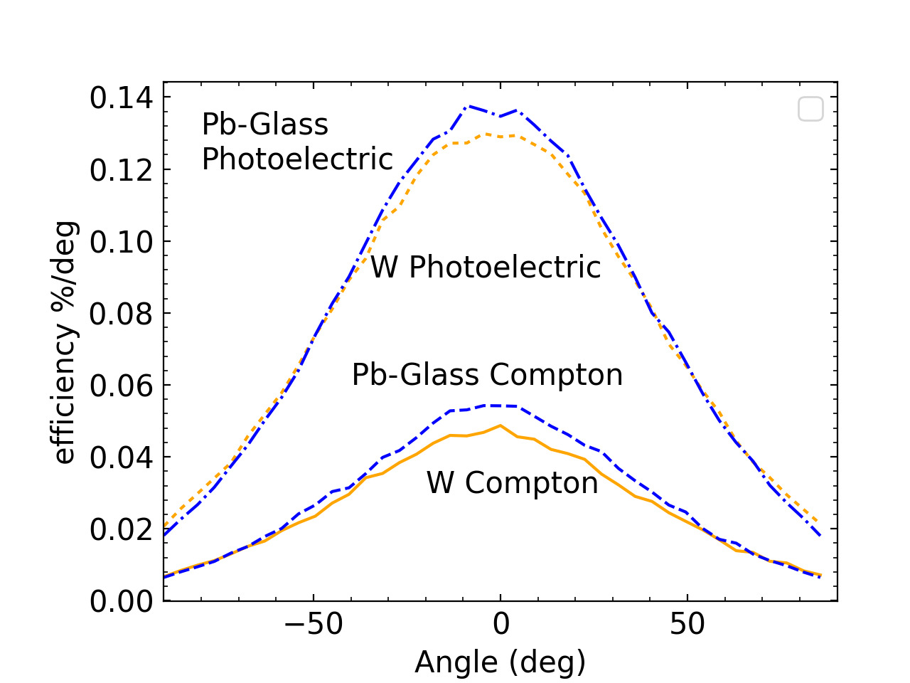
Figure 5 shows the predicted electron angular distributions from the exit side of a thin plate from a 511 keV gamma ray at normal incidence. The plate thickness for lead-glass is 150 microns (0.006”) and for W is 50 microns (0.002”).
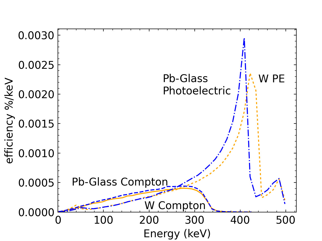
The predicted electron energy spectrum from the exit side of a thin plate from a 511 keV gamma ray at normal incidence is shown in Figure 6. The respective plate thicknesses are 150 microns (0.006”) and 50 microns (0.002”) for lead-glass and W. The structures below 500 keV are due to the atomic K and L shells.
6.2 Surface Direct Production of a Primary Electron
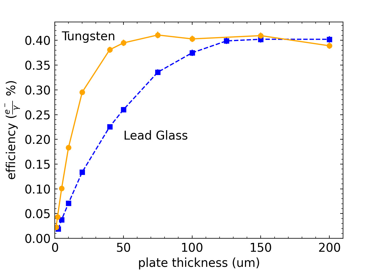
The predicted electron yield per 511 KeV gamma ray traversing a thin sheet of lead-glass (dashed) and W (solid) at normal incidence versus plate thickness in microns is shown in Figure 7. The yield is for the exit side of the plate. The lower density of the glass is compensated by the larger depth from which electrons reach the surface. We take as nominal values for the thickness at which the curve has reached its plateau as 150 microns for lead-glass and 50 microns for W.
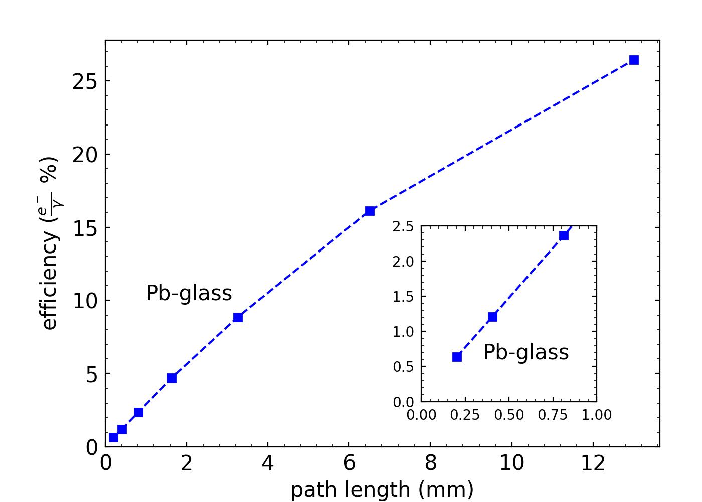
Figure 8 shows the efficiency for the production of an electron that exits a lamina through either surface versus the projected path length of a 511 keV gamma ray travelling inside a lead-glass lamina substrate of thickness 150 microns (0.006”). Note that the efficiency in lead-glass is 25% at a slab thickness of 1.27 cm (1/2”) and grows approximately linearly, as one would expect.
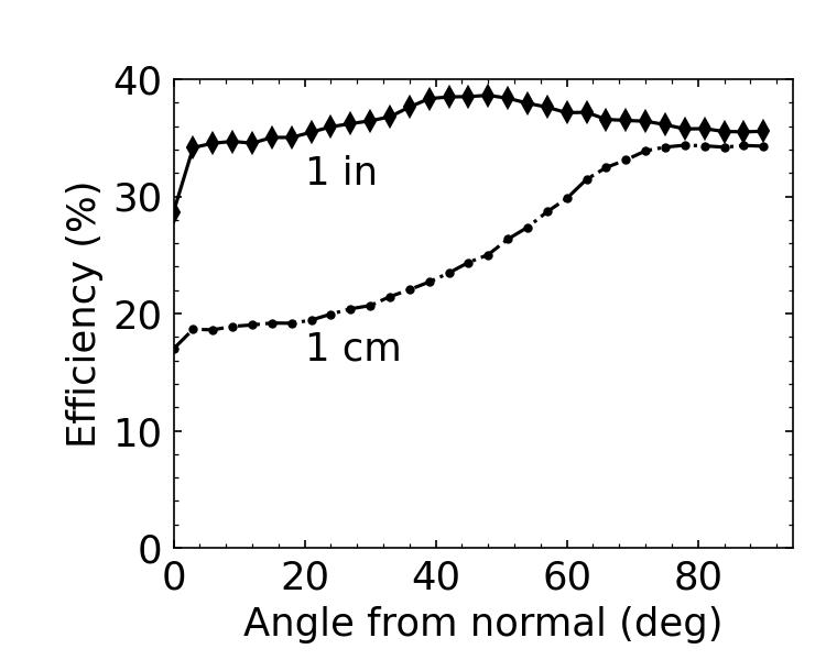
Figure 9 shows the efficiency for 1 cm-thick and 2.54 cm-thick LMCPs for conversion of a 511 keV gamma ray to a primary electron that traverses a channel wall into the channel interior, crossing at least one layer of secondary-emission material, versus incident gamma ray angle. Thinner LMCPs will have better time resolution; thicker will have higher efficiency.
7 Summary
We have studied a laminated microchannel plate (LMCP) formed by assembling thin laminae, rather than the conventional method of assembling and drawing fibers. An LMCP channel plate is assembled from laminae with one or both sides patterned with channels that extend from one edge of the lamina (corresponding to the top surface of the LMCP) to the other edge (the LMCP bottom). The channels can be patterned in both transverse and longitudinal directions. Options include entrance funnels, patterns of strike surfaces, and an exit ‘choke.’
We have used the TOPAS simulation framework to determine the parameters and efficiency for the surface direct conversion of 511 keV gamma rays to electrons in a micro-channel plate (LMCP) constructed from thin laminae of lead-glass patterned with micro-channels. Direct conversion of the gamma ray to an electron eliminates the common two-step process of first converting of the gamma ray into an optical photon in a scintillator, followed by the conversion of the photon into an electron in a photodetector. The simulations predict an efficiency for conversion of 511 keV gamma rays of 30% for a single 2.54 cm-thick lead-glass LMCP; multiple units can be stacked for higher efficiencies. The elimination of a photocathode allows assembly at atmospheric pressure.
The shape of each thin lamina determines the local dimensions of the LMCP, allowing non-uniform cross-sections in slab thickness, width, and length. The slab can be non-planar, allowing curved surfaces in both lateral dimensions.
The channels can be patterned on laminae surfaces with customized internal shapes, textures and structure. The channel-forming surfaces can be functionalized with resistive, secondary-emissive, and conducting coatings with patterns and thicknesses selected for specific applications. The channels need not be parallel nor uniform across the LMCP, for example in concave/convex LMCPs for focusing, or LMCPs in rapidly varying rate environments such as close to an accelerator beam.
The laminar construction allows incorporating structural elements directly in the LMCP. Tabs can be added to the lamina perimeter to provide precision alignment and internal support against atmospheric pressure in large-area multi-module vacuum vessels such as planes of pre-shower samplers in particle physics, or in large area radially-thin cylindrical geometries in TOF-PET.
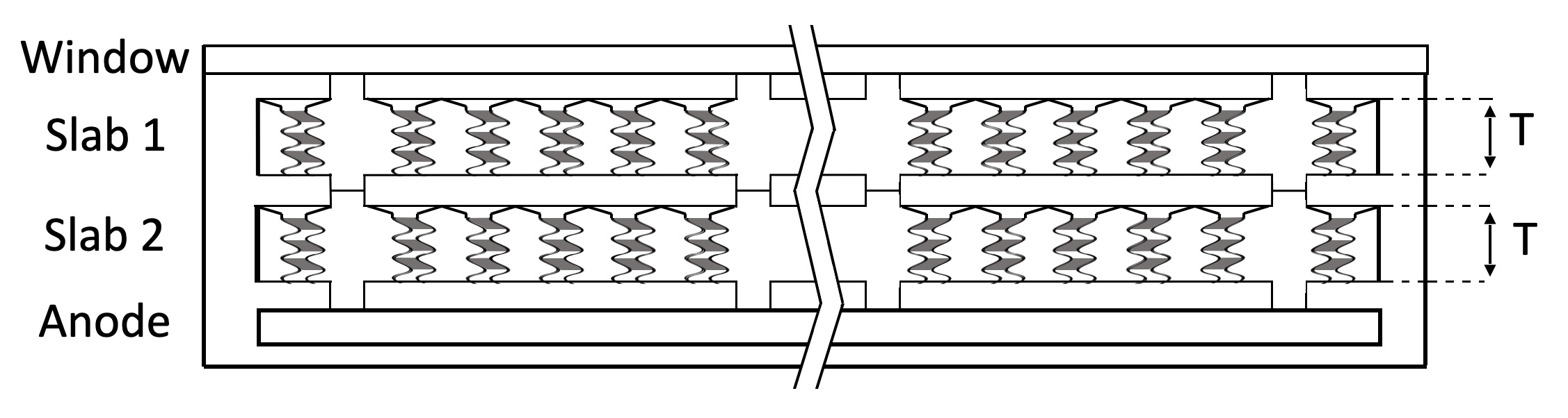
Figure 10 shows an example detector assembly with two LMCPs in series. We note that as the primary electron from the gamma ray may cross a channel at any point along the channel length, the gain in a slab varies event-to-event. This variable gain can be ameliorated by positioning the dynodes at the exit end of the channel, or by adding a conventional non-converting MCP operated in saturation as the final amplifier in the stack of components.
Acknowledgments
We thank Joseph Perl for the exemplary development of TOPAS and for remarkable user support. We are indebted to Mary Heintz for essential computational system development and advice, and to Ian Goldberg and Justin Gurvitch for crucial graphics contributions.
For financial support of undergraduate research from University of Chicago College, Physical Sciences Division, and Enrico Fermi Institute, we thank Steven Balla and Nichole Fazio, Michael Grosse, and Scott Wakely, respectively.
References
-
[1]
S. Vandenberghe, P. Moskal, J. S. Karp;
State of the art in total body PET
EJNMMI Phys. 2020 May 25;7(1):35. doi: 10.1186/s40658-020-00290-2. - [2] J. J. Vaquero and P. Kinahan; Positron Emission Tomography: Current Challenges and Opportunities for Technological Advances in Clinical and Preclinical Imaging Systems Annual Review of Biomedical Engineering Volume 17, 385; (2015)
-
[3]
M. E. Phelps, S. R. Cherry, and M.
Dahlbom;
PET: Physics,instrumentation, and scanners; Springer New York (2006)
doi.org/10.1007/0-387-34946-4 -
[4]
S. Vandenberghe, P. Moskal, J.S. Karp;
State of the art in total body PET
EJNMMI Phys. 2020 May 25;7(1):35.
doi: 10.1186/s40658-020-00290-2. PMID: 32451783; PMCID: PMC7248164. -
[5]
R. D. Badawi, H. Shi, and S. R. Cherry et al.
First Human Imaging Studies with the EXPLORER Total-Body PET Scanner;
J Nucl Med. 2019 Mar; 60(3): 299-303. doi: 10.2967/jnumed.119.226498 -
[6]
Z. Insepov, V. Ivanov, S.
J. Jokela, I. V. Veryovkin and A. V. Zinovev;
Comparison of secondary electron emission simulation to experiment; Nucl. Instr. Meth A639, 155 (2011) - [7] J.L. Wiza, Micro-channel Plate Detectors. Nuclear Instruments and Methods 162, 1979, pp 587-601
- [8] K. Domurat-Sousa, C. Poe; Methods for Simulating Low-Z-Medium-based TOF-PET in TOPAS; Submitted to Nucl. Instr. and Meth., June, 2023
-
[9]
B. Faddegon, J. Ramos-Mendez, J. Schuemann, J. Shin, J. Perl, H.
Paganetti
The TOPAS tool for particle simulation, a Monte Carlo simulation tool for physics, biology and clinical research; European Journal of Medical Physics; Volume 72, P114-121, April (2020); DOI:https://doi.org/10.1016/j.ejmp.2020.03.019 - [10] B.W. Adams, A. Elagin, H. Frisch, R. Obaid, E. Oberla, A. Vostrikov, R. Wagner, J. Wang, M. Wetstein; Timing Characteristics of Large Area Picosecond Photodetectors; Nucl. Inst. Meth. Phys. Res. A. , Vol. 795, pp 1-11 (Sept. 2015)
-
[11]
E. Angelico, T. Seiss, B. W, Adams, A. Elagin, H. J. Frisch, E. Spieglan;
Capacitively coupled pickup in MCP-based photo-detectors using a conductive, metallic anode; Nucl. Inst. Meth. Phys. Res. A. (Oct. 2016) - [12] Jinseo Park, Fangjian Wu, Evan Angelico, Henry J. Frisch, Eric Spieglan; Patterned anodes with sub-millimeter spatial resolution for large-area MCP-based photodetector systems Nuclear Inst. and Methods in Physics Research, A 985 (2021) 164702; 22 Sept, 2020
- [13] J.-F. Genat, G. Varner, F. Tang, H. Frisch; Signal Processing for Pico-second Resolution Timing Measurements; Nucl.Instrum.Meth.A607:387-393,Oct., 2009. arXiv:0810.5590
-
[14]
E. Oberla, J.-F. Genat, H. Grabas, H. Frisch, K. Nishimura, and G. Varner;
A 15 GSa/s, 1.5 GHz Bandwidth Waveform Digitizing ASIC;
Nucl. Instr. Meth. A735, 21 Jan., 2014, 452 - [15] E. Oberla; PSEC4 waveform sampler and Large-Area Picosecond Photo-Detectors readout electronics: Procedings of the Workshop on Picosecond Photon Sensors, Clermont-Ferrand, 2014. Available at http://lappddocs.uchicago.edu/documents/243