Intrinsic Nonlinear Hall Detection of the Néel Vector for Two-Dimensional Antiferromagnetic Spintronics
Abstract
The respective unique merit of antiferromagnets and two-dimensional (2D) materials in spintronic applications inspire us to exploit 2D antiferromagnetic spintronics. However, the detection of the Néel vector in 2D antiferromagnets remains a great challenge because the measured signals usually decrease significantly in the 2D limit. Here we propose that the Néel vector of 2D antiferromagnets can be efficiently detected by the intrinsic nonlinear Hall (INH) effect which exhibits unexpected significant signals. As a specific example, we show that the INH conductivity of the monolayer manganese chalcogenides Mn (=S, Se, Te) can reach the order of nmmA/V2, which is orders of magnitude larger than experimental values of paradigmatic antiferromagnetic spintronic materials. The INH effect can be accurately controlled by shifting the chemical potential around the band edge, which is experimentally feasible via electric gating or charge doping. Moreover, we explicitly demonstrate its -periodic dependence on the Néel vector orientation based on an effective model. Our findings enable flexible design schemes and promising material platforms for spintronic memory device applications based on 2D antiferromagnets.
Introduction.—The desire to reduce the size and power consumption of spintronic devices stimulated the emergence of a new field referred to as two-dimensional (2D) spintronics Avsar et al. (2020); Zhang et al. (2019); Li and Wu (2016); Lin et al. (2019); Ahn (2020); Han (2016). Two-dimensional materials with atomic thickness have attracted extraordinary interest in spintronics because they not only provide a promising opportunity to push the relevant devices to the 2D limit, but also enable the hopeful exploration of new spintronic phenomena due to their unusual spin-dependent properties, such as the spin-valley coupling of transition metal dichalcogenides Xiao et al. (2012) and the spin-momentum locking of quantum spin Hall insulators Kane and Mele (2005). However, almost all the existing 2D materials proposed for spintronics are nonmagnetic or ferromagnetic Zhang et al. (2021) (e.g., CrI3 Huang et al. (2017) and CrGeTe3 Gong et al. (2017)). In this Letter, we extend the 2D spintronics to antiferromagnets and show that the Néel vector, which serves as a state variable for 2D antiferromagnetic spintronics, can be detected by the nonlinear Hall measurement.
Antiferromagnets composed of antiferromagnetically coupled magnetic elements are attractive for spintronics because of their faster dynamics, zero stray fields, and insensitivity to magnetic perturbations Baltz et al. (2018); Jungwirth et al. (2016). The robust high-speed manipulation of the Néel vector Železný et al. (2014); Manchon et al. (2019), such as ultrafast 90∘ switching by current-induced spin-orbit toque Wadley et al. (2016); Olejník et al. (2017); Bodnar et al. (2018); Roy et al. (2016); Olejník et al. (2018) and reproducible 180∘ reversal by flipping the polarity of the writing current Wadley et al. (2018); Godinho et al. (2018), have been demonstrated in recent experiments. However, the failure of Néel vector detections via conventional magnetic techniques due to the absence of net magnetization poses a major challenge for practical applications of antiferromagnetic spintronics Baltz et al. (2018). Several optical and microscopic methods, such as the spin-polarized scanning tunneling microscopy Wortmann et al. (2001), the x-ray magnetic linear dichroism microscopy Grzybowski et al. (2017a), the femtosecond pump-probe magneto-optical experiment Saidl et al. (2017), the spatially resolved second-harmonic generation Sun et al. (2019); Ni et al. (2021), and the diamond nitrogen-vacancy scanning probe magnetometry Erickson et al. (2023) work for accurate detection of Néel vector, but are difficult to incorporate for high-density integration devices. The anisotropic magnetoresistance (AMR) effect is useful for experimental detection of a 90∘ rotation but is invariant upon a 180∘ reversal of the Néel vector, and its small magnitude limits the readout speed and the possible miniaturization Železný et al. (2018). Recently, the reversed Néel vector states are electrically distinguished by a second-order magnetoresistance effect Godinho et al. (2018); Wang et al. (2021); Liu et al. (2021), but has been limited in bulk materials. Since the readout speed and size scalability is usually proportional to the magnitude of the response signal which could significantly diminish in the ultimate atomic limit Jungwirth et al. (2016, 2018), it is, therefore, natural to raise the question: how to efficiently detect the Néel vector with significantly large readout signal for 2D antiferromagnetic spintronics?
In this Letter, we predict that the Néel vector of 2D antiferromagnets can be efficiently read out using the INH effect which exhibits a significant signal that can be detected by experimental means. Taking 2D manganese chalcogenide Mn (=S, Se, Te) as an example, we show that the INH conductivity of the MnS monolayer can reach the order of nm mA/V2, which is orders-of-magnitude larger than the experimentally measured values of typical antiferromagnets CuMnAs Godinho et al. (2018); Wang et al. (2021) and Mn2Au Liu et al. (2021). The INH effect can be controlled by shifting the chemical potential via electric gating or charge doping. We further develop an effective model to explain its dependence on the Néel vector direction with a periodicity. Together with the efficient write-in approach based on current-induced spin-orbit toques, our findings constitute promising design schemes and material platforms for 2D antiferromagnetic spintronics.
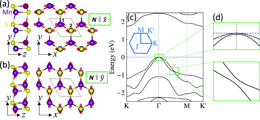
Atomic and band structures.—Due to similar crystal structures of 2D Mn, which have been successfully synthesized in experiments Aapro et al. (2021), we take MnS as an example hereafter and defer the rest to the Supplemental Material 111See Supplemental Material at http://link.aps.org/supplemental/xxx, for more details about the derivation of the effective Hamiltonian and the numerical calculation of INH effect, which include Refs. Kresse and Furthmüller (1996); Mostofi et al. (2008); Godinho et al. (2018). As shown in Fig. 1(a), MnS crystallizes in an AA-stacked bilayer honeycomb lattice, where Mn (and ) atoms on top and bottom layers (Mn1 and Mn2) occupy opposite sublattices. The lattice structure belongs to the space group of (No. 164, ). Our first-principles calculations ††footnotemark: show that the magnetic moments are about 4.36 per Mn atom and are antiferromagnetically ordered, which are consistent with previous studies Sattar et al. (2022). The Néel vector , which is defined as the difference of the magnetic moments between Mn1 and Mn2 in the unit-cell, shows a significant in-plane anisotropy with the magnetocrystalline anisotropy energy being about 0.4 meV per unit-cell. For lying in different in-plane directions, there is little energy difference (see Fig. S5 ††footnotemark: ), indicating that it is possible to electrically manipulate by current pulses via spin-orbit torques Grzybowski et al. (2017b); Godinho et al. (2018); Bodnar et al. (2018, 2019). More importantly, for an arbitrary direction of , which is denoted by its polar angle with respect to the -axis, the combination of spatial and time reversal symmetry () is respected.
Figure 1(c) shows the calculated band structure for 2D MnS with . Because of the symmetry, every band is doubly degenerate. It is noted that some nearly degenerate points (NDPs) lie at at the valence band maximum and along the line around eV. Since the valence bands are dominated by the S-p orbitals, the weak spin-orbit coupling of S only induces slight band splitting at the NDPs [see Fig. 1(d)] compared to MnSe and MnTe ††footnotemark: , which plays a crucial role for the INH effect, as we will discuss later.
INH effect in MnS.— In general, the nonlinear Hall conductivity tensor is defined as the quadratic current response to electric field : , where are Cartesian indices. The nonlinear Hall conductivity can be separated into time-reversal-even (-even) and -odd parts, but only the latter can be utilized to detect the Néel vector reversal. In 2D antiferromagnets respecting the symmetry, the -even Berry curvature dipole (BCD) contribution is strictly forbidden Nandy and Sodemann (2019); Ma et al. (2019). In contrast, the -odd INH conductivity which is allowed becomes an ideal quantity for the Néel vector detection, and is therefore our main concern. The INH conductivity can be expressed in terms of band quantities as Gao et al. (2014); Gao and Xiao (2018)
| (1) | |||||
| (2) | |||||
| (3) |
where is the Berry-connection polarizability (BCP) and [] is the (band-resolved) BCP dipole. is the Berry connection with the periodic part of the th Bloch state, is the energy of the th Bloch state, is the band velocity, is the Fermi-Dirac distribution for energy at the chemical potential , and is the dimension of the system.
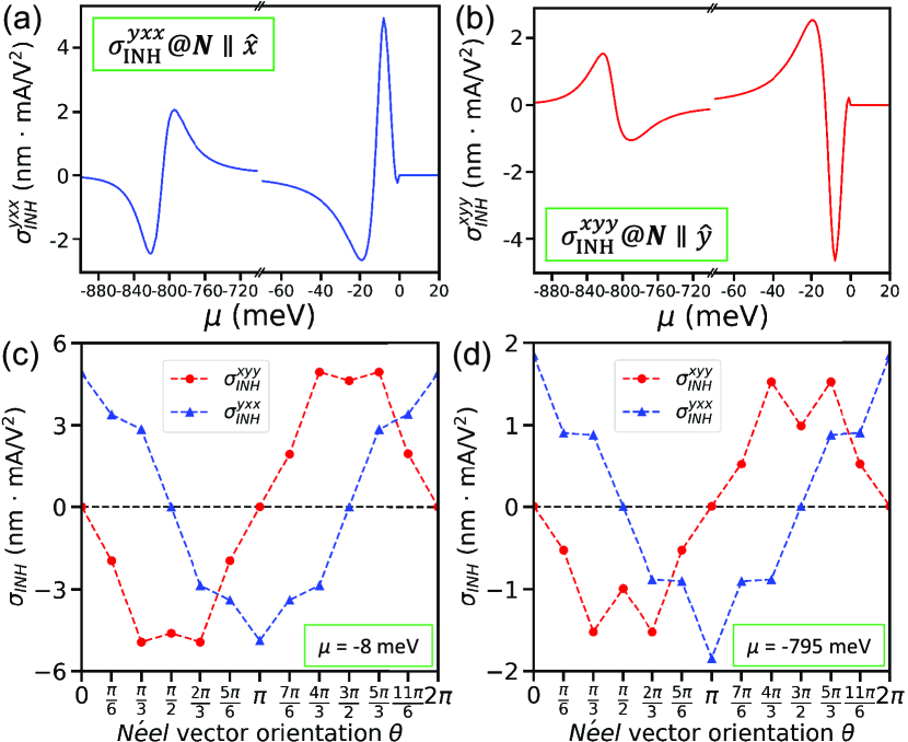
We first analyze the symmetry constraint on . Taking as an example, the magnetic configuration belongs to the magnetic space group. The allowed components are , and , while the rest vanishes ††footnotemark: . Given that the Hall bar for transport measurements of 2D materials is usually set up within the plane, we focus on the in-plane component () with along the direction for describing the INH effect in 2D MnS. Figures 2(a) and 2(b) show the calculated as a function of the chemical potential . For a down-shift of upon hole doping, and exhibit significant peaks with opposite signs at and meV near the band edge, and at , and meV which are close to the NDPs along the - line. This signifies that the dominant contributions of are from these small-gap regions. Remarkably, when is along the () direction, the peaks of () are on the order of nmmA/V2.
It is worth noting that despite the atomically ultrathin 2D nature, the significant value of in MnS is two orders of magnitude larger than the values reported in antiferromagnetic CuMnAs Godinho et al. (2018); Wang et al. (2021) and Mn2Au Liu et al. (2021) ( nmmA/V2), which are prototype materials of antiferromagnetic memory devices. The peak value of in MnS is even comparable to the large in -invariant few-layer WTe2 Kang et al. (2019); Wang and Qian (2019). In practice, the carrier doping for 2D materials ( cm-2) can be conveniently controlled by electric gating Ma et al. (2019); Williams et al. (2007); Chen et al. (2010); Efetov and Kim (2010); Velasco et al. (2016), electron-beam irradiation Shi et al. (2020); Choi et al. (2021) or remote modulation Lee et al. (2021); Zhao et al. (2017). We, therefore, expect that it is experimentally feasible to measure our predicted INH effect in the 2D antiferromagnet MnS.
Next, we show that depends sensitively on the direction of . As shown in Figs. 2(c) and 2(d), both and exhibit a periodicity when rotates in the plane, which satisfies the -odd constraint that . The angular dependence of is approximately described by cosine or sine trigonometric functions. Therefore, the reorientation of can be fully detected by measuring the INH effect, which is a unique merit over the conventional AMR-based approach that cannot distinguish a 180∘ reversal. In particular, the sign of () can be used to distinguish reversal in direction ( or ) [in direction ( or )]. Therefore, the INH effect can serve as a powerful tool for detecting .
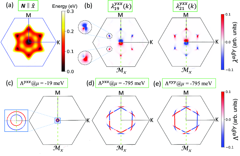
To gain underlying insight into the behavior of , we analyze the band-resolved BCP dipole , which exhibits the contribution to from each band. Similar to other band geometric quantities such as the Berry curvature, encodes the interband coherence. Figure 3(a) shows the energy difference between the top two valence bands, where one NDP at and six along - lines can be observed. In addition, the small-gap region forms a snowflakelike shape centered at . These NDPs give rise to small denominators for the BCP in Eq. (3) and hence a large contribution to for the top two valance bands, as shown in Fig. 3(b).
Due to the derivative of the Fermi-Dirac function in Eq. (1), is a Fermi surface property. Therefore, only NDPs close to make significant contributions to . To examine the -resolved contribution for different peaks, we plot the distribution of the BCP dipole for different peaks of , as shown in Figs. 3(c) and 3(d). The calculated at meV mainly distributes around , while the dominant contribution to at meV comes from the small-gap region including the rest NDPs. This indicates that a large can be achieved by tuning towards such regions.
As shown in Fig. 3(c)-(e), despite complicated sign changes of , it is actually an even function with respect to - due to the additional constraint from crystalline symmetries for . On the contrary, is dictated to be an odd function with respect to [see Fig. 3(e)], which leads to the vanishment of at (and ) [see Fig. 2(d)]. Similarly, for , becomes an even function with respect to -, but the preserved symmetry demands to be an odd function (see Fig. S9 ††footnotemark: ). Although the distribution of seems unaltered when rotates from to , our detailed analysis indicates that it delicately changes to satisfy different symmetry constraints, which results in distinct after integrating over the whole Brillouin zone.
Effective model.—To better understand the Néel vector orientation dependence of in MnS, we construct an effective model to describe the top two valence bands around . To do so, we first establish an effective model with symmetry and then consider the antiferromagnetism by introducing opposite Zeeman exchange fields for two sublattices. We can start from the antibonding and bonding states of S- orbitals on two sublattices, , where indicates orbitals and for spin. We label the sub-lattice, orbital, and spin degree of freedom with Pauli matrices , and , respectively. The symmetry operations of group are represented as: , mirror symmetry , inversion symmetry , time reversal symmetry , where is complex conjugate operator. In this representation, the full eight-band Hamiltonian reads,
| (4) |
where are antibonding/bonding subspace Hamiltonian, couples two sublattices, and is the coupling of orbitals within one sublattice (see Supplemental Material ††footnotemark: ). The last term represents the Zeeman exchange field where is the coupling strength and represents the Néel vector orientation. To describe the top two valence bands, we then downfold the Hamiltonian to the anti-bonding subspace based on the Löwding perturbation method Winkler (2003); Huang et al. (2013), which yields
| (5) | |||||
where . are material-dependent parameters, among which and represent the SOC induced band splitting. are related to antiferromagnetism.
As a simple illustration, let us consider the case of [i.e., ]. Keeping up to the lowest order of , we arrive at
| (6) | ||||
This is a tilted massive Dirac model where is the SOC-induced mass controlling the gap and represents the AFM-induced tile of the Dirac cone. The energy spectrum is given by . In this model, the nonvanishing component is which exhibits two peaks with opposite signs when approaches the small-gap region, which is consistent with our first-principles calculations in Fig. 2(a). Because the quadratic terms of , which would bend over the upper valence band significantly, are neglected in the above model (6), the quantitative discrepancy would be eliminated once these terms are included (see Fig. S1-S2 ††footnotemark: ).
More interestingly, when rotates in the x-y plane with a polar angle with respect to the -axis, it is convenient to obtain the effective model by a coordinate transformation. Consequently, the transform as
| (7) | |||||
| (8) |
which is consistent with the -dependent behavior of in Fig. 2(c). Similarly, for at meV, we construct an effective model with 3 pairs of overtilted massive Dirac cones Huang et al. (2016); Yan et al. (2017) that are related by symmetry, and the angular dependence of is attributed to the -dependent tilts that are not canceled within Dirac cone pairs ††footnotemark: . Thus, the effective model qualitatively explains the large at small-gap regions and its special angular dependence in MnS. These features of the INH effect should be generally expected for 2D -symmetric antiferromagnets with similar band structures.
Discussion and summary.—In usual Hall measurements with a planar geometry of the setup, the applied electric field may be along a general direction instead of aligning with the crystal axes. When one applies an in-plane electric field where is the polar angle with respect to the -axis, the measured in-plane INH current (along the perpendicular direction) is
| (9) |
where the angle-dependent INH conductivity is
| (10) |
The INH conductivity is maximized (minimized) when and are parallel (anti-parallel), but vanishes when they are perpendicular.
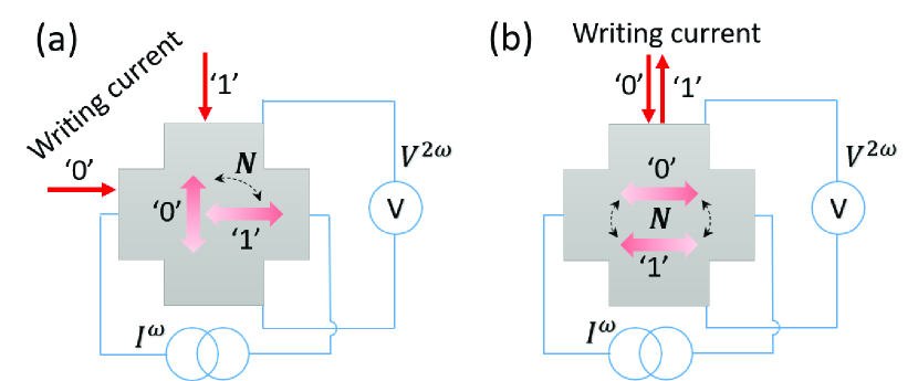
The above functionality motivates us to propose a 2D antiferromagnetic memory device based on the standard Hall bar setup. As shown in Fig. 4, reversible orthogonal switching or 180∘ reversal of , which represents two memory states, can be controlled by applying the writing current along two orthogonal directions Wadley et al. (2016); Olejník et al. (2017); Bodnar et al. (2018); Zhou et al. (2018); Meinert et al. (2018) or flipping its polarity Godinho et al. (2018); Wadley et al. (2018). In both schemes, the INH detection of can be performed by injecting a probing current with frequency and measuring the transverse voltage with double frequency , which has been implemented in previous nonlinear Hall measurements Ma et al. (2019); Kang et al. (2019); Du et al. (2018); Huang et al. (2022); He and Weng (2021); Duan et al. (2022); He et al. (2022); Zhang et al. (2022). However, the two states in Fig. 4(a) [4(b)] are represented by zero and finite signals (two opposite signals).
In summary, we have predicted the INH detection of in 2D antiferromagnets Mn, which provides a promising material platform and efficient electric readout approach for 2D antiferromagnetic spintronics. Combined with the high-speed write-in scheme using picosecond current pulses, it is possible to achieve ultra-fast and multi-level memory device applications based on 2D antiferromagnets. For example, a six-level triaxial memory with parallel or anti-parallel to three equivalent axes of MnS can be constructed since it is now able to distinguish these states and their reversed images via the INH effect. In addition, the vast number of 2D antiferromagnetic semiconductors, such as MnPS3 Chittari et al. (2016); Chu et al. (2020); Sivadas et al. (2016); Ni2021imaging, TaCoTe2 Li et al. (2019), Fe2TeO6 and SrFe2S2O Zhao et al. (2022), bilayer Fe3GeTe2 Yang et al. (2021) and CrCl3 Cai et al. (2019), hold great promise for future research.
Acknowledgements.
This work was supported by the National Key R&D Program of China (Grant No. 2021YFA1401600), the National Natural Science Foundation of China (Grant No. 12074006), and the start-up fund from Peking University. H.Z. and W.D. acknowledge support from the Basic Science Center Project of NSFC (Grant No. 51788104), the Ministry of Science and Technology of China, and the Beijing Advanced Innovation Center for Future Chip (ICFC). The computational resources were supported by the high-performance computing platform of Peking University and the National Supercomputer Center in Guangzhou (NSCC-GZ). J.W. and H.Z. contributed equally to this work.References
- Avsar et al. (2020) A. Avsar, H. Ochoa, F. Guinea, B. Özyilmaz, B. J. van Wees, and I. J. Vera-Marun, “Colloquium: Spintronics in graphene and other two-dimensional materials,” Rev. Mod. Phys. 92, 021003 (2020).
- Zhang et al. (2019) Wen Zhang, Ping Kwan Johnny Wong, Rui Zhu, and Andrew T. S. Wee, “Van der waals magnets: Wonder building blocks for two-dimensional spintronics?” InfoMat 1, 479–495 (2019).
- Li and Wu (2016) Xiuling Li and Xiaojun Wu, “Two-dimensional monolayer designs for spintronics applications,” WIRES: Comp. Mol. Sci. 6, 441–455 (2016).
- Lin et al. (2019) Xiaoyang Lin, Wei Yang, Kang L. Wang, and Weisheng Zhao, “Two-dimensional spintronics for low-power electronics,” Nature Electronics 2, 274–283 (2019).
- Ahn (2020) Ethan C. Ahn, “2d materials for spintronic devices,” npj 2D Materials and Applications 4, 17 (2020).
- Han (2016) Wei Han, “Perspectives for spintronics in 2d materials,” APL Materials 4, 032401 (2016).
- Xiao et al. (2012) Di Xiao, Gui-Bin Liu, Wanxiang Feng, Xiaodong Xu, and Wang Yao, “Coupled spin and valley physics in monolayers of and other group-vi dichalcogenides,” Phys. Rev. Lett. 108, 196802 (2012).
- Kane and Mele (2005) C. L. Kane and E. J. Mele, “Quantum spin hall effect in graphene,” Phys. Rev. Lett. 95, 226801 (2005).
- Zhang et al. (2021) Shuqing Zhang, Runzhang Xu, Nannan Luo, and Xiaolong Zou, “Two-dimensional magnetic materials: structures, properties and external controls,” Nanoscale 13, 1398–1424 (2021).
- Huang et al. (2017) Bevin Huang, Genevieve Clark, Efrén Navarro-Moratalla, Dahlia R. Klein, Ran Cheng, Kyle L. Seyler, Ding Zhong, Emma Schmidgall, Michael A. McGuire, David H. Cobden, Wang Yao, Di Xiao, Pablo Jarillo-Herrero, and Xiaodong Xu, “Layer-dependent ferromagnetism in a van der waals crystal down to the monolayer limit,” Nature 546, 270–273 (2017).
- Gong et al. (2017) Cheng Gong, Lin Li, Zhenglu Li, Huiwen Ji, Alex Stern, Yang Xia, Ting Cao, Wei Bao, Chenzhe Wang, Yuan Wang, Z. Q. Qiu, R. J. Cava, Steven G. Louie, Jing Xia, and Xiang Zhang, “Discovery of intrinsic ferromagnetism in two-dimensional van der waals crystals,” Nature 546, 265–269 (2017).
- Baltz et al. (2018) V. Baltz, A. Manchon, M. Tsoi, T. Moriyama, T. Ono, and Y. Tserkovnyak, “Antiferromagnetic spintronics,” Rev. Mod. Phys. 90, 015005 (2018).
- Jungwirth et al. (2016) T. Jungwirth, X. Marti, P. Wadley, and J. Wunderlich, “Antiferromagnetic spintronics,” Nat. Nanotechnol. 11, 231–241 (2016).
- Železný et al. (2014) J. Železný, H. Gao, K. Výborný, J. Zemen, J. Mašek, Aurélien Manchon, J. Wunderlich, Jairo Sinova, and T. Jungwirth, “Relativistic néel-order fields induced by electrical current in antiferromagnets,” Phys. Rev. Lett. 113, 157201 (2014).
- Manchon et al. (2019) A. Manchon, J. Železný, I. M. Miron, T. Jungwirth, J. Sinova, A. Thiaville, K. Garello, and P. Gambardella, “Current-induced spin-orbit torques in ferromagnetic and antiferromagnetic systems,” Rev. Mod. Phys. 91, 035004 (2019).
- Wadley et al. (2016) P. Wadley, B. Howells, J. Železný, C. Andrews, V. Hills, R. P. Campion, V. Novák, K. Olejník, F. Maccherozzi, S. S. Dhesi, S. Y. Martin, T. Wagner, J. Wunderlich, F. Freimuth, Y. Mokrousov, J. Kuneš, J. S. Chauhan, M. J. Grzybowski, A. W. Rushforth, K. W. Edmonds, B. L. Gallagher, and T. Jungwirth, “Electrical switching of an antiferromagnet,” Science 351, 587–590 (2016).
- Olejník et al. (2017) K. Olejník, V. Schuler, X. Marti, V. Novák, Z. Kašpar, P. Wadley, R. P. Campion, K. W. Edmonds, B. L. Gallagher, J. Garces, M. Baumgartner, P. Gambardella, and T. Jungwirth, “Antiferromagnetic CuMnAs multi-level memory cell with microelectronic compatibility,” Nat. Commun. 8, 15434 (2017).
- Bodnar et al. (2018) S. Yu Bodnar, L. Šmejkal, I. Turek, T. Jungwirth, O. Gomonay, J. Sinova, A. A. Sapozhnik, H. J. Elmers, M. Kläui, and M. Jourdan, “Writing and reading antiferromagnetic mn2au by néel spin-orbit torques and large anisotropic magnetoresistance,” Nat. Commun. 9, 348 (2018).
- Roy et al. (2016) P. E. Roy, R. M. Otxoa, and J. Wunderlich, “Robust picosecond writing of a layered antiferromagnet by staggered spin-orbit fields,” Phys. Rev. B 94, 014439 (2016).
- Olejník et al. (2018) K. Olejník, T. Seifert, Z. Kašpar, V. Novák, P. Wadley, R. P. Campion, M. Baumgartner, P. Gambardella, P. Němec, J. Wunderlich, J. Sinova, Kužel P., M. Müller, T. Kampfrath, and T Jungwirth, “Terahertz electrical writing speed in an antiferromagnetic memory,” Sci. Adv. 4, eaar3566 (2018).
- Wadley et al. (2018) Peter Wadley, Sonka Reimers, Michal J. Grzybowski, Carl Andrews, Mu Wang, Jasbinder S. Chauhan, Bryan L. Gallagher, Richard P. Campion, Kevin W. Edmonds, Sarnjeet S. Dhesi, Francesco Maccherozzi, Vit Novak, Joerg Wunderlich, and Tomas Jungwirth, “Current polarity-dependent manipulation of antiferromagnetic domains,” Nat. Nanotechnol. 13, 362–365 (2018).
- Godinho et al. (2018) J Godinho, H Reichlová, D Kriegner, V Novák, K Olejník, Z Kašpar, Z Šobáň, P Wadley, RP Campion, RM Otxoa, et al., “Electrically induced and detected Néel vector reversal in a collinear antiferromagnet,” Nat. Commun. 9, 4686 (2018).
- Wortmann et al. (2001) D. Wortmann, S. Heinze, Ph. Kurz, G. Bihlmayer, and S. Blügel, “Resolving complex atomic-scale spin structures by spin-polarized scanning tunneling microscopy,” Phys. Rev. Lett. 86, 4132–4135 (2001).
- Grzybowski et al. (2017a) M. J. Grzybowski, P. Wadley, K. W. Edmonds, R. Beardsley, V. Hills, R. P. Campion, B. L. Gallagher, J. S. Chauhan, V. Novak, T. Jungwirth, F. Maccherozzi, and S. S. Dhesi, “Imaging current-induced switching of antiferromagnetic domains in cumnas,” Phys. Rev. Lett. 118, 057701 (2017a).
- Saidl et al. (2017) V Saidl, P Němec, P Wadley, V Hills, RP Campion, V Novák, KW Edmonds, F Maccherozzi, SS Dhesi, BL Gallagher, et al., “Optical determination of the néel vector in a cumnas thin-film antiferromagnet,” Nature Photonics 11, 91–96 (2017).
- Sun et al. (2019) Zeyuan Sun, Yangfan Yi, Tiancheng Song, Genevieve Clark, Bevin Huang, Yuwei Shan, Shuang Wu, Di Huang, Chunlei Gao, Zhanghai Chen, et al., “Giant nonreciprocal second-harmonic generation from antiferromagnetic bilayer cri3,” Nature 572, 497–501 (2019).
- Ni et al. (2021) Zhuoliang Ni, A. V. Haglund, H. Wang, B. Xu, C. Bernhard, D. G. Mandrus, X. Qian, E. J. Mele, C. L. Kane, and Liang Wu, “Imaging the néel vector switching in the monolayer antiferromagnet mnpse3 with strain-controlled ising order,” Nat. Nanotechnol. 16, 782–787 (2021).
- Erickson et al. (2023) Adam Erickson, Syed Qamar Abbas Shah, Ather Mahmood, Ilja Fescenko, Rupak Timalsina, Christian Binek, and Abdelghani Laraoui, “Nanoscale imaging of antiferromagnetic domains in epitaxial films of cr2o3 via scanning diamond magnetic probe microscopy,” RSC Adv. 13, 178–185 (2023).
- Železný et al. (2018) J. Železný, P. Wadley, K. Olejník, A. Hoffmann, and H. Ohno, “Spin transport and spin torque in antiferromagnetic devices,” Nat. Phys. 14, 220–228 (2018).
- Wang et al. (2021) Chong Wang, Yang Gao, and Di Xiao, “Intrinsic nonlinear hall effect in antiferromagnetic tetragonal cumnas,” Phys. Rev. Lett. 127, 277201 (2021).
- Liu et al. (2021) Huiying Liu, Jianzhou Zhao, Yue-Xin Huang, Weikang Wu, Xian-Lei Sheng, Cong Xiao, and Shengyuan A. Yang, “Intrinsic second-order anomalous hall effect and its application in compensated antiferromagnets,” Phys. Rev. Lett. 127, 277202 (2021).
- Jungwirth et al. (2018) T. Jungwirth, J. Sinova, A. Manchon, X. Marti, J. Wunderlich, and C. Felser, “The multiple directions of antiferromagnetic spintronics,” Nat. Phys. 14, 200–203 (2018).
- Aapro et al. (2021) Markus Aapro, Md. Nurul Huda, Jeyakumar Karthikeyan, Shawulienu Kezilebieke, Somesh C. Ganguli, Héctor González Herrero, Xin Huang, Peter Liljeroth, and Hannu-Pekka Komsa, “Synthesis and properties of monolayer mnse with unusual atomic structure and antiferromagnetic ordering,” ACS Nano 15, 13794–13802 (2021).
- Note (1) See Supplemental Material at http://link.aps.org/supplemental/xxx, for more details about the derivation of the effective Hamiltonian and the numerical calculation of INH effect, which include Refs. Kresse and Furthmüller (1996); Mostofi et al. (2008); Godinho et al. (2018).
- Sattar et al. (2022) Shahid Sattar, M. F. Islam, and C. M. Canali, “Monolayer and janus (, se, te): A family of two-dimensional antiferromagnetic semiconductors,” Phys. Rev. B 106, 085410 (2022).
- Grzybowski et al. (2017b) M. J. Grzybowski, P. Wadley, K. W. Edmonds, R. Beardsley, V. Hills, R. P. Campion, B. L. Gallagher, J. S. Chauhan, V. Novak, T. Jungwirth, F. Maccherozzi, and S. S. Dhesi, “Imaging Current-Induced Switching of Antiferromagnetic Domains in CuMnAs,” Phys. Rev. Lett. 118, 057701 (2017b).
- Bodnar et al. (2019) S. Yu. Bodnar, M. Filianina, S. P. Bommanaboyena, T. Forrest, F. Maccherozzi, A. A. Sapozhnik, Y. Skourski, M. Kläui, and M. Jourdan, “Imaging of current induced néel vector switching in antiferromagnetic ,” Phys. Rev. B 99, 140409 (2019).
- Nandy and Sodemann (2019) Snehasish Nandy and Inti Sodemann, “Symmetry and quantum kinetics of the nonlinear hall effect,” Phys. Rev. B 100, 195117 (2019).
- Ma et al. (2019) Qiong Ma, Su-Yang Xu, Huitao Shen, David MacNeill, Valla Fatemi, Tay-Rong Chang, Andrés M. Mier Valdivia, Sanfeng Wu, Zongzheng Du, Chuang-Han Hsu, Shiang Fang, Quinn D. Gibson, Kenji Watanabe, Takashi Taniguchi, Robert J. Cava, Efthimios Kaxiras, Hai-Zhou Lu, Hsin Lin, Liang Fu, Nuh Gedik, and Pablo Jarillo-Herrero, “Observation of the nonlinear Hall effect under time-reversal-symmetric conditions,” Nature 565, 337–342 (2019).
- Gao et al. (2014) Yang Gao, Shengyuan A. Yang, and Qian Niu, “Field Induced Positional Shift of Bloch Electrons and Its Dynamical Implications,” Phys. Rev. Lett. 112, 166601 (2014).
- Gao and Xiao (2018) Yang Gao and Di Xiao, “Orbital magnetic quadrupole moment and nonlinear anomalous thermoelectric transport,” Phys. Rev. B 98, 060402 (2018).
- Kang et al. (2019) Kaifei Kang, Tingxin Li, Egon Sohn, Jie Shan, and Kin Fai Mak, “Nonlinear anomalous hall effect in few-layer wte2,” Nat. Mater. 18, 324–328 (2019).
- Wang and Qian (2019) Hua Wang and Xiaofeng Qian, “Ferroelectric nonlinear anomalous hall effect in few-layer wte2,” npj Computational Materials 5, 119 (2019).
- Williams et al. (2007) J. R. Williams, L. DiCarlo, and C. M. Marcus, “Quantum hall effect in a gate-controlled p-n junction of graphene,” Science 317, 638–641 (2007).
- Chen et al. (2010) J. Chen, H. J. Qin, F. Yang, J. Liu, T. Guan, F. M. Qu, G. H. Zhang, J. R. Shi, X. C. Xie, C. L. Yang, K. H. Wu, Y. Q. Li, and L. Lu, “Gate-voltage control of chemical potential and weak antilocalization in ,” Phys. Rev. Lett. 105, 176602 (2010).
- Efetov and Kim (2010) Dmitri K. Efetov and Philip Kim, “Controlling electron-phonon interactions in graphene at ultrahigh carrier densities,” Phys. Rev. Lett. 105, 256805 (2010).
- Velasco et al. (2016) Jairo Jr. Velasco, Long Ju, Dillon Wong, Salman Kahn, Juwon Lee, Hsin-Zon Tsai, Chad Germany, Sebastian Wickenburg, Jiong Lu, Takashi Taniguchi, Kenji Watanabe, Alex Zettl, Feng Wang, and Michael F. Crommie, “Nanoscale control of rewriteable doping patterns in pristine graphene/boron nitride heterostructures,” Nano Lett. 16, 1620–1625 (2016).
- Shi et al. (2020) Wu Shi, Salman Kahn, Lili Jiang, Sheng-Yu Wang, Hsin-Zon Tsai, Dillon Wong, Takashi Taniguchi, Kenji Watanabe, Feng Wang, Michael F. Crommie, and Alex Zettl, “Reversible writing of high-mobility and high-carrier-density doping patterns in two-dimensional van der waals heterostructures,” Nature Electronics 3, 99–105 (2020).
- Choi et al. (2021) Min Sup Choi, Myeongjin Lee, Tien Dat Ngo, James Hone, and Won Jong Yoo, “Chemical dopant-free doping by annealing and electron beam irradiation on 2d materials,” Advanced Electronic Materials 7, 2100449 (2021).
- Lee et al. (2021) Donghun Lee, Jea Jung Lee, Yoon Seok Kim, Yeon Ho Kim, Jong Chan Kim, Woong Huh, Jaeho Lee, Sungmin Park, Hu Young Jeong, Young Duck Kim, and Chul-Ho Lee, “Remote modulation doping in van der waals heterostructure transistors,” Nature Electronics 4, 664–670 (2021).
- Zhao et al. (2017) Yuda Zhao, Kang Xu, Feng Pan, Changjian Zhou, Feichi Zhou, and Yang Chai, “Doping, contact and interface engineering of two-dimensional layered transition metal dichalcogenides transistors,” Adv. Funct. Mater. 27, 1603484 (2017).
- Winkler (2003) Roland Winkler, Spin—Orbit Coupling Effects in Two-Dimensional Electron and Hole Systems, Vol. 191 (Springer Nature, Switzerland AG, 2003).
- Huang et al. (2013) Huaqing Huang, Wenhui Duan, and Zhirong Liu, “The existence/absence of dirac cones in graphynes,” New J. Phys. 15, 023004 (2013).
- Huang et al. (2016) Huaqing Huang, Shuyun Zhou, and Wenhui Duan, “Type-ii dirac fermions in the class of transition metal dichalcogenides,” Phys. Rev. B 94, 121117 (2016).
- Yan et al. (2017) Mingzhe Yan, Huaqing Huang, Kenan Zhang, Eryin Wang, Wei Yao, Ke Deng, Guoliang Wan, Hongyun Zhang, Masashi Arita, Haitao Yang, Zhe Sun, Hong Yao, Yang Wu, Shoushan Fan, Wenhui Duan, and Shuyun Zhou, “Lorentz-violating type-ii dirac fermions in transition metal dichalcogenide ptte2,” Nat. Commun. 8, 257 (2017).
- Zhou et al. (2018) X. F. Zhou, J. Zhang, F. Li, X. Z. Chen, G. Y. Shi, Y. Z. Tan, Y. D. Gu, M. S. Saleem, H. Q. Wu, F. Pan, and C. Song, “Strong orientation-dependent spin-orbit torque in thin films of the antiferromagnet ,” Phys. Rev. Applied 9, 054028 (2018).
- Meinert et al. (2018) Markus Meinert, Dominik Graulich, and Tristan Matalla-Wagner, “Electrical switching of antiferromagnetic and the role of thermal activation,” Phys. Rev. Applied 9, 064040 (2018).
- Du et al. (2018) Z. Z. Du, C. M. Wang, Hai-Zhou Lu, and X. C. Xie, “Band signatures for strong nonlinear hall effect in bilayer ,” Phys. Rev. Lett. 121, 266601 (2018).
- Huang et al. (2022) Meizhen Huang, Zefei Wu, Jinxin Hu, Xiangbin Cai, En Li, Liheng An, Xuemeng Feng, Ziqing Ye, Nian Lin, Kam Tuen Law, and Ning Wang, “Giant nonlinear Hall effect in twisted bilayer WSe2,” Natl. Sci. Rev. (2022), 10.1093/nsr/nwac232, nwac232.
- He and Weng (2021) Zhihai He and Hongming Weng, “Giant nonlinear hall effect in twisted bilayer wte2,” npj Quantum Materials 6, 101 (2021).
- Duan et al. (2022) Junxi Duan, Yu Jian, Yang Gao, Huimin Peng, Jinrui Zhong, Qi Feng, Jinhai Mao, and Yugui Yao, “Giant second-order nonlinear hall effect in twisted bilayer graphene,” Phys. Rev. Lett. 129, 186801 (2022).
- He et al. (2022) Pan He, Gavin Kok Wai Koon, Hiroki Isobe, Jun You Tan, Junxiong Hu, Antonio H. Castro Neto, Liang Fu, and Hyunsoo Yang, “Graphene moiré superlattices with giant quantum nonlinearity of chiral bloch electrons,” Nat. Nanotechnol. 17, 378–383 (2022).
- Zhang et al. (2022) Cheng-Ping Zhang, Jiewen Xiao, Benjamin T. Zhou, Jin-Xin Hu, Ying-Ming Xie, Binghai Yan, and K. T. Law, “Giant nonlinear hall effect in strained twisted bilayer graphene,” Phys. Rev. B 106, L041111 (2022).
- Chittari et al. (2016) Bheema Lingam Chittari, Youngju Park, Dongkyu Lee, Moonsup Han, Allan H. MacDonald, Euyheon Hwang, and Jeil Jung, “Electronic and magnetic properties of single-layer metal phosphorous trichalcogenides,” Phys. Rev. B 94, 184428 (2016).
- Chu et al. (2020) Hao Chu, Chang Jae Roh, Joshua O. Island, Chen Li, Sungmin Lee, Jingjing Chen, Je-Geun Park, Andrea F. Young, Jong Seok Lee, and David Hsieh, “Linear magnetoelectric phase in ultrathin probed by optical second harmonic generation,” Phys. Rev. Lett. 124, 027601 (2020).
- Sivadas et al. (2016) Nikhil Sivadas, Satoshi Okamoto, and Di Xiao, “Gate-controllable magneto-optic kerr effect in layered collinear antiferromagnets,” Phys. Rev. Lett. 117, 267203 (2016).
- Li et al. (2019) Si Li, Ying Liu, Zhi-Ming Yu, Yalong Jiao, Shan Guan, Xian-Lei Sheng, Yugui Yao, and Shengyuan A. Yang, “Two-dimensional antiferromagnetic dirac fermions in monolayer ,” Phys. Rev. B 100, 205102 (2019).
- Zhao et al. (2022) Hong Jian Zhao, Xinran Liu, Yanchao Wang, Yurong Yang, Laurent Bellaiche, and Yanming Ma, “Zeeman effect in centrosymmetric antiferromagnetic semiconductors controlled by an electric field,” Phys. Rev. Lett. 129, 187602 (2022).
- Yang et al. (2021) Xiuxian Yang, Xiaodong Zhou, Wanxiang Feng, and Yugui Yao, “Strong magneto-optical effect and anomalous transport in the two-dimensional van der waals magnets (, 4, 5),” Phys. Rev. B 104, 104427 (2021).
- Cai et al. (2019) Xinghan Cai, Tiancheng Song, Nathan P. Wilson, Genevieve Clark, Minhao He, Xiaoou Zhang, Takashi Taniguchi, Kenji Watanabe, Wang Yao, Di Xiao, Michael A. McGuire, David H. Cobden, and Xiaodong Xu, “Atomically thin crcl3: An in-plane layered antiferromagnetic insulator,” Nano Lett. 19, 3993–3998 (2019).
- Kresse and Furthmüller (1996) G. Kresse and J. Furthmüller, “Efficiency of ab-initio total energy calculations for metals and semiconductors using a plane-wave basis set,” Comput. Mater. Sci. 6, 15 (1996).
- Mostofi et al. (2008) Arash A Mostofi, Jonathan R Yates, Young-Su Lee, Ivo Souza, David Vanderbilt, and Nicola Marzari, “wannier90: A tool for obtaining maximally-localised wannier functions,” Comput. Phys. Commun. 178, 685–699 (2008).