[1]Institute of Advanced Technology, University of Science and Technology of China, Hefei, Anhui, 230026, P. R. China \affil[2]Institute of Artificial Intelligence, Hefei Comprehensive National Science Center, Hefei, Anhui, 230026, P. R. China \affil[3]CAS Key Laboratory of Quantum Information, University of Science and Technology of China, Hefei, Anhui, 230026, P. R. China \affil[4]CAS Center For Excellence in Quantum Information and Quantum Physics, University of Science and Technology of China, Hefei, Anhui, 230026, P. R. China \affil[5]Hefei National Laboratory, Hefei, Anhui, 230088, P. R. China \affil[6]Origin Quantum Computing Company Limited, Hefei, Anhui, 230026, P. R. China
Resource-Efficient Circuit Compilation for SWAP Networks
Abstract
The SWAP network offers a promising solution for addressing the limited connectivity in quantum systems by mapping logical operations to physically adjacent qubits. In this article, we present a novel decomposition strategy for the SWAP network, accompanied by additional extensions that leverage an overcomplete set of native gates. Through comprehensive evaluations, we demonstrate the effectiveness of our protocol in reducing the gate count and streamlining the implementation of generalized SWAP networks and Quantum Random Access Memory (QRAM). Our research tackles the challenges posed by limited connectivity, leading to improved performance of SWAP networks and simplified QRAM implementation, thereby contributing to the advancement of quantum computing technologies.
1 Introduction
Near-term quantum computers [1] have made promising progress [2, 3, 4, 5], particularly in superconducting quantum processors [6]. Meanwhile, existing quantum algorithms have demonstrated the potential for achieving quantum speedup [7, 8]. However, these algorithms are developed using high-level abstractions [9], where quantum circuits are designed with arbitrary connectivity. This creates a mismatch between the required connectivity for the algorithms and the actual connectivity provided by quantum devices, leading to the need for additional resources [10, 11]. The existence of this disparity presents a significant hurdle because current quantum devices exhibit two-qubit gate error rates ranging from 1% to 5% [12], which requires additional operations as less as possible. Therefore, it is imperative to address this challenge in order to achieve the promised speedup.
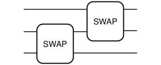
The SWAP network [13, 14] is a prominent choice for facilitating interactions between non-adjacent qubits in superconducting quantum processors [15, 16, 17]. However, the standard quantum assembly language (QASM) compilation of SWAP involves 3 CNOT gates [18], as depicted in the bottom left of Fig. 1, thereby increasing the circuit depth. Moreover, the CNOT is still not a native gate [19] for superconducting qubits coupled by X-Y interaction, i.e. tunable superconducting qubits. To transform each CNOT into a native CZ gate, two additional Hadamard gates are required [20]. Consequently, it is crucial to design a decomposition strategy utilizing native gates [19, 21] to compile SWAP networks and minimize the experimental overhead on the platform of tunable superconducting qubits.
To tackle these challenges, recent research has demonstrated improved performance by employing native gate sets for simplified decomposition of SWAP gates and enhanced efficiency of SWAP networks [22, 23, 24, 25]. As highlighted in [23], the SWAP has been transpiled into 3 three native two-qubit gates, SYC gate. This decomposition strategy still incurs considerable overhead, but introducing additional native two-qubit gates into the gate set for SWAP decomposition, as demonstrated by [22] can reduce circuit depth by approximately 30% compared to using only CZ gates. At the same time, another approach achieves a reduction of around 60% in errors during quantum algorithm implementation [25]. Nevertheless, the significant calibration overhead associated with single-qubit gates and the interleaved structure of single and two-qubit gates indicates further room for improvement.
In this article, we present a novel approach to decompose SWAP networks using a set of native gates , which are operations directly available in the tunable superconducting qubits [26, 27].
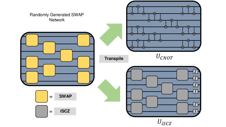
Firstly, we utilize this two-qubit native gate set to decompose the SWAP gate. Our approach offers significant advantages in terms of reducing gate count and circuit depth by compared to the standard QASM version. Additionally, we extend this protocol by incorporating information about initial states and circuit topology, further enhancing its effectiveness. Secondly, we demonstrate the practical applications of our decomposition strategy in two scenarios. We conduct numerical experiments on random SWAP networks utilizing our decomposition strategy. Then, we implement the QRAM circuit [28, 29] incorporating both mentioned extensions.
This paper is organized as follows. Section 2 presents our resource-efficient decomposition protocol for SWAP networks. Section 3 explores the application of our SWAP network decomposition approach to various quantum algorithms. And Section 4 concludes the article by summarizing the results and highlighting future research directions. The appendix provides comprehensive derivations of our decomposition strategy, accompanied by illustrative figures.
2 Methods
In this section, we first demonstrate the decomposition of the SWAP gate using the native two-qubit gate set . Then, we integrate this decomposition strategy for the SWAP gate into the SWAP network. Lastly, we explore the extensions brought about by our newly proposed strategy.

2.1 Optimized SWAP Network
The iSWAP and CZ gates are fundamental and native operations in tunable superconducting qubits. The iSWAP gate exchanges the states of two qubits while introducing a phase factor, while the CZ gate applies a controlled-phase operation. These gates commute with each other, as in Eq. 1, allowing for their interchangeable usage.
| (1) |
The iSCZ gate, defined as shown in Eq. 1 and 2, is derived from the combination of the iSWAP and CZ gates.
| (2) |
which follows the properties .
This implies that the decomposition of the SWAP gate, previously requiring three CNOT operations, can now be achieved using two two-qubit native operations. A parametrized native two-qubit gate, fSim, proposed and realized by the Google team [6], offers greater flexibility in implementing two-qubit gates.
| (3) |
and . If the gate, or the iSCZ operation, is accessible and can be directly implemented on the superconducting circuit, it indicates that SWAP that used to take 3 two-qubit gates now only need one . It would greatly facilitate the realization of the single SWAP gate.
In general, considering neighboring qubits , are two neighboring qubits in a circuit with arbitrary topology, denoted as , we have the following relations:
| (4) | ||||
The Eq. 1 can be easily verified. Furthermore, we have observed,
| (5) |
The commutation relation in Eq. 5 enables the rearrangement of phase gates that appear after each iSCZ gate. This flexibility is a crucial element for optimizing the decomposition of SWAP networks.
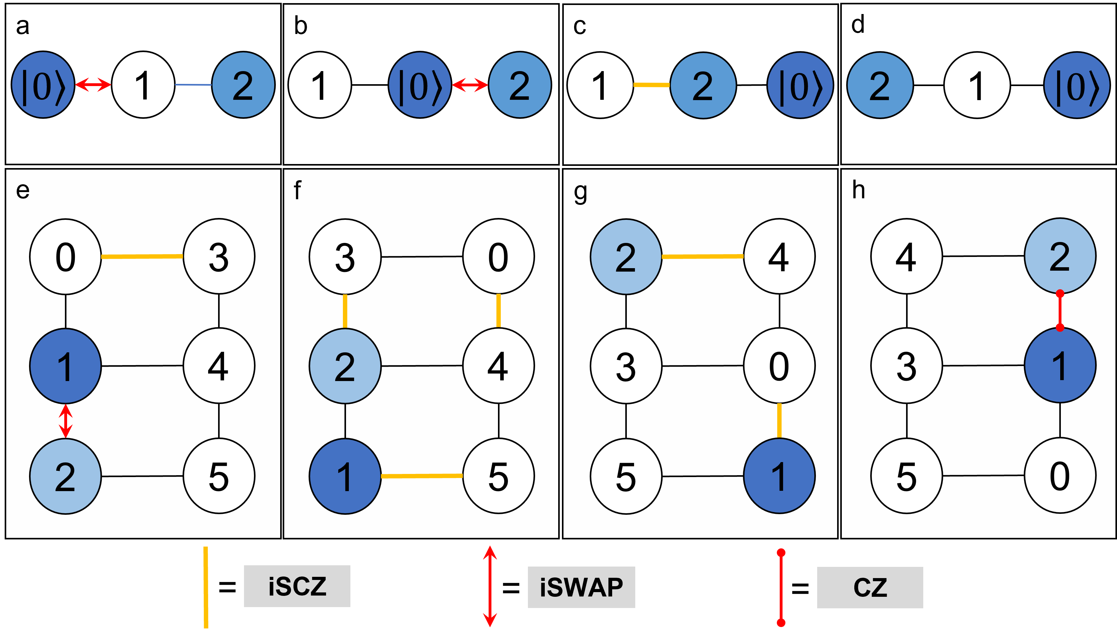
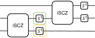
To achieve an equivalent -qubit SWAP network using iSCZ gates, as shown in Fig. 2, the following steps need to be taken:
-
1.
Replace all SWAP gates with iSCZ gates in the exact same positions.
-
2.
Count the number of SWAP gates along the swap path for each qubit .
-
3.
Apply single-qubit gates to the final position of each qubit .

In a SWAP network, replacing a SWAP with iSCZ would induce one phase gate on each qubit it involves. This increases the circuit depth and introduces 2 more single qubit gates, resulting in longer execution time and higher susceptibility to decoherence. However, by utilizing Eq. 5, we are able to move phase gates for possible cancellation, therefore, reducing the circuit depth and total gate count. In our strategy for SWAP networks, we choose to move all single phase gates after all iSCZ gates, like in Fig. 2.
We observe that sequences of multiple phase gates follow periodic patterns of 4, and , . This allows us to reduce the number of single-qubit gates from to for an -qubit SWAP network with SWAPs. The additional depth caused by single-qubit gates for the SWAP network in our strategy is only 1 now.
The overall process is summarized as an algorithm. The input, represented by the list Path consists of a sequence of SWAPs that can realize the desired SWAP network. Each element in the list, , is a tuple of indices of two qubits involved in the SWAP. The output Phase decides the type of phase gate to be applied to each qubit.

2.2 Extensions
There are several extensions available to further reduce the gate count and, consequently, achieve a lower circuit depth.
2.2.1 Extension 1
Firstly, it is observed that iSWAP and are capable of replacing the SWAP completely without CZ when or is because . This substitution is crucial to the case where one of the qubits before the SWAP network stays in the state up to a phase, such as Fig.4 in [30].
2.2.2 Extension 2
Furthermore, this decomposition provides increased flexibility in scheduling CZs during practical implementations. When replacing SWAPs with iSWAPs and CZs, the CZ could be implemented not only at the exact moment of the SWAP but also at any time when two qubits involved in the SWAP are nearest neighbors. This arises from the fact that actual information and remains unchanged throughout the entire process of the SWAP network. Thus, as long as they become nearest neighbors, the can always be achieved by the CZ.
Consequently, CZ gates can be implemented in advance or with a delay. By leveraging this flexibility, the CZs can be rearranged in parallel with other operations within the SWAP network, or used to absorb other two-qubit operations preceding and following the SWAP network. This allows for the reduction of the overall circuit depth, as the CZ gates can be integrated more efficiently into the surrounding operations.
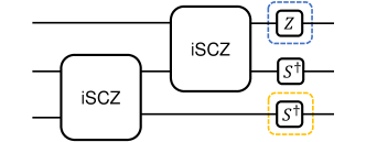
In general, the algorithm 1 sharply reduces the number of two-qubit operations from to in an -qubit SWAP network containing SWAPs, when the operation iSCZ is experimentally feasible. Even with the currently available two-qubit gate set [22], the algorithm achieves approximately reduction in circuit depth. The additional cost of single-qubit gates is limited to , as depicted in Fig. 3. The specific benefits of the two extensions may vary depending on the particular case at hand.
3 Application
In this section, we will apply our strategy to address two problems that involve a significant number of SWAP operations, making our method particularly suitable for their practical implementations. Firstly, we will conduct numerical experiments on random SWAP networks to demonstrate how our strategy improves the decomposition process. By analyzing the results, we can observe the benefits of our approach in terms of reduced gate count and circuit depth. Secondly, we will provide a comprehensive analysis of QRAM and assess its experimental feasibility. Additionally, we will explore the potential resource savings achieved by utilizing our decomposition strategy in the implementation of QRAM.
3.1 Generalized SWAP networks for NISQ
The concept of a generalized SWAP network was introduced in [14]. It serves the purpose of not only enabling the mapping of logical qubits to physical qubits but also supporting the mapping of fermionic modes to physical qubits for Hamiltonian simulations.
In our numerical experiments, we focus on a specific type of SWAP network known as a 2-complete linear SWAP network. In this network, all pairs of logical qubits are arranged linearly, and SWAP gates are applied exclusively to physically adjacent qubits.
The numerical experiments are conducted as follows: given a size , an initial list is initialized, and a random permutation of these integers is generated, resulting in a new list . The value at the -th index of the new list represents the information previously stored in the -th qubit of the initial layout. Once the permutation is fixed, the routing path and the sequence of SWAP gates can be determined.
Within the routing SWAP network, two different strategies for decomposing SWAP gates are considered: one replaces all SWAP gates with CNOT gates, while the other utilizes iSWAP and CZ gates. The same level of noise is applied to all two-qubit native operations. For each size , the experiment is repeated 100 times, resulting in 100 random permutations and corresponding layouts.
The recorded metrics include the circuit depth and the state fidelity
| (6) |
for both noiseless and noisy circuits, where and denote the density matrix states before and after the application of noise, respectively. In the case of noiseless circuits, where the density matrix states before and after the application of SWAP networks are pure states (), the expression of fidelity simplifies to . The experimental results are presented below in detail.

We conducted a comparative analysis between two categories: circuit depth and fidelity. Our method consistently generates circuits with lower depth compared to the alternative approach across various sizes of swap networks. As the system size increases, the disparity in circuit depth becomes more pronounced. Additionally, our method exhibits a distinct advantage in terms of fidelity. While the fidelity gradually decreases due to noise, our approach demonstrates a slower decline compared to the alternative method.
Our numerical experiment results provide compelling evidence to demonstrate the advantages of our strategy. Collectively, our method consistently achieves lower circuit depths and maintains higher fidelity across a broad spectrum of system sizes. These findings underline the significance of our approach in improving the efficiency and reliability of SWAP networks.
3.2 QRAM Implementation
The QRAM enables the coherent superposition-based access of addresses and retrieval of classical data from a quantum computer. The task of an (n, k)-QRAM, involving the retrieval of classical data with a word length of from one of the addresses , can be described by a unitary operation as follows:
| (7) |
where the address register consists of qubits, and the data register consists of qubits.
However, QRAMs are computationally expensive and often require resources, posing scalability challenges. To address this issue, the bucket-brigade structure was proposed [31], which significantly reduces the number of ancillary qubits needed for QRAMs, achieving a time complexity of . Additionally, a recent protocol [29] claims an improved time complexity of instead of , achieving linear growth in both the word and address lengths.
Two operations are repeatedly employed in QRAM implementations [29]. The first is the Internal-SWAP operation. It alters the state of all address registers within a layer based on the data register of the corresponding node and the address register of its parent node. The Routing operation exchanges the information between the parent node with one of its child nodes based on the status of its address register. It is worth noting that the bidirectional Routing assumes one of the two nodes to be in the state, while the unidirectional version does not have such an assumption.
3.2.1 Layer Representation
Due to the unique design of QRAM, we can simplify the expressions of two operations at the layer level. The full description of layer , , is now where . The net effect of the operation can be written as:
| (8) |
Here, the 3-2-SWAP operation is defined specifically for qutrit-qubit nodes and accomplishes the transitions and .
Similarly, the could be simplified as,
| (9) |
where the node has the only non-zero address register in -th layer. If the address register of the node in the QRAM is qubit instead of qutrit, there will be a minor change in the Internal-SWAP,
| (10) |
while the Routing operation remains the same, as in Fig. 7.

3.2.2 Practical Implementations of QRAMs with optimizations
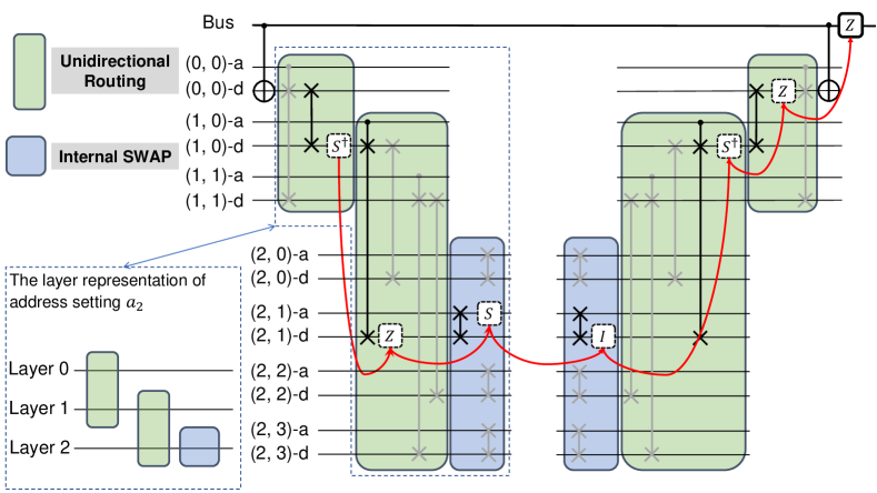
In the frame of layers, Routings and Internal-SWAPs are acting like SWAPs, therefore our strategy could further simplify the circuit implementation. First, because of the difference between uni- and bidirectional Routings, the implementation of unidirectional could be simplified into pairs of SWAP and Controlled-SWAP (C-SWAP) instead of pairs of C-SWAPs, as shown in Fig. 9. The rest of the optimizations enabled by our strategy has been demonstrated below.
Phase Shifts and Correction
Two types of phase shifts arise when replacing SWAP and C-SWAP gates with the iSWAP-CZ (iSCZ) gates and both of them adhere to Eq. 1. The first type of shifts accumulates on the address register due to the unidirectional Routings and Internal-SWAPs during the address setting and uncomputing phase, such as the phases represented by on the of Fig. 8 when the address data is . In this case, no matter which direction the data move within layers, it will experience at most one C-SWAP or SWAP and accumulate one more phase error . This particular type of shifts can be rectified during the uncomputing stage as it returns to the bus along with the address data only with the count of unidirectional Routings and Internal-SWAPs it has experienced. For example, this number is 6 in Fig. 8 as highlighted in green rounded corner rectangular boxes.
The second type of shifts persists on the data registers and propagates across layers due to both uni- and bidirectional Routings. Fig. 9 illustrates an example of how these shifts are transferred during the process of loading data . However, it is not possible to correct those errors all at once like the first type due to the classical copy operation that occurs at the end of the binary tree. Therefore, the phase shifts on the data prior to copying can be corrected on the bus prior to loading it into the binary tree, while the phase error on the data after interaction with classical memory can be corrected on the bus after exiting the binary tree.
In these two separate phases, the logic is the same as what happens to the error on address registers, which is that it only takes the count of Routings for each data to correct the phase errors.
Additionally, the two extensions described earlier are fully applicable in the QRAM implementation.
Extension 1
All iSCZ and C-iSCZ in unidirectional Routings, wherein only one target qubit of the SWAP carries useful information, could be further simplified as iSWAP and C-iSWAP(iFredkin) without the additional CZs and CCZs. This simplification significantly reduces the gate complexity and enhances the efficiency of the QRAM structure [32, 33, 34, 35].
Extension 2
However, there exists a small subset of bidirectional Routings gates where two qubits store the data and respectively. Consequently, it is not possible to completely replace the bidirectional SWAP gates with iSWAP gates and single-qubit phase gates alone. In such cases, CZ gates, as proposed in Section 2, are still necessary.
| (11) | ||||
where .
During the transfer of data , it will meet data that have interacted with the classical memory cells. It will accumulate for not doing the CZ and CCZ immediately. Taking inspiration from the method described in section 2.2, each term can be realized by a single CZ gate within the Quantum Processing Unit (QPU) when the logical qubits containing and are nearest neighbors, rather than within the QRAM structure itself. Similarly, the term is achieved by introducing an additional CCZ gate during the data copy operation, which is shown in the Fig. 9 in the gray round corner rectangular.

In conclusion, our method provides a transformation of the original QRAM structure described in [29]. Instead of utilizing SWAP and C-SWAP gates, our method replaces them with C-iSWAP and iSWAP gates with additional CCZ gates in the classical copy operations and CZs on QPU. This modification allows for a more efficient and optimized implementation of the QRAM, reducing the gate complexity and improving overall performance.
4 Summary and Outlook
In this paper, we have presented a novel strategy for decomposing the SWAP network, which involves an over-complete set of two-qubit native gates. Our approach significantly reduces the cost associated with decomposing SWAP gates by approximately . By substituting all SWAP gates with iSCZ gates, along with a layer of single qubit phase gates, instead of relying solely on CNOTs, CZs, or iSWAPs, we can effectively handle more complex SWAP networks.
Moreover, two extensions enabled by our strategy offer promising opportunities for optimizing SWAP networks. These extensions leverage the benefits of our approach and provide additional flexibility for various scenarios. Notably, our method proves particularly advantageous for QRAMs under specific assumptions. By minimizing the number of required two-qubit native operations, our approach brings QRAMs closer to practical implementation while delivering overall improvements to SWAP networks.
There are many works to be done under the framework of our method. The flexible arrangement of single-qubit phase gates offers the potential for improved compilation time by moving those single-qubit gates alongside two-qubit gates applied to other qubits [36, 37]. Additionally, considering the native operations allows us to take into account various physical restrictions, including the presence of unwanted yet unavoidable noise sources [38]. Incorporating these considerations into the decomposition process will contribute to advancing the performance of quantum algorithms in actual quantum devices.
5 Acknowledgement
This work was supported by the National Natural Science Foundation of China (Grant No. 12034018), and Innovation Program for Quantum Science and Technology No. 2021ZD0302300. The numerical experiments are coded in Python using the QISKit library [39]. We thank Cheng Xue for the helpful discussions.
References
- [1] John Preskill. Quantum Computing in the NISQ era and beyond. Quantum, 2:79, August 2018.
- [2] Han-Sen Zhong, Hui Wang, Yu-Hao Deng, et al. Quantum computational advantage using photons. Science, 370(6523):1460–1463, 2020.
- [3] Lars S Madsen, Fabian Laudenbach, Mohsen Falamarzi Askarani, et al. Quantum computational advantage with a programmable photonic processor. Nature, 606(7912):75–81, June 2022.
- [4] Mohsin Iqbal, Nathanan Tantivasadakarn, Ruben Verresen, Sara L Campbell, Joan M Dreiling, Caroline Figgatt, John P Gaebler, Jacob Johansen, Michael Mills, Steven A Moses, Juan M Pino, Anthony Ransford, Mary Rowe, Peter Siegfried, Russell P Stutz, Michael Foss-Feig, Ashvin Vishwanath, and Henrik Dreyer. Creation of non-abelian topological order and anyons on a trapped-ion processor. 2023.
- [5] C. Monroe and J. Kim. Scaling the ion trap quantum processor. Science, 339(6124):1164–1169, 2013.
- [6] F. Arute, K. Arya, R. Babbush, et al. Quantum supremacy using a programmable superconducting processor. Nature, 574(7779):505–510, 2019.
- [7] Lov K. Grover. A fast quantum mechanical algorithm for database search. In Proceedings of the Twenty-Eighth Annual ACM Symposium on Theory of Computing, STOC ’96, page 212–219, New York, NY, USA, 1996. Association for Computing Machinery.
- [8] Peter W. Shor. Polynomial-time algorithms for prime factorization and discrete logarithms on a quantum computer. SIAM Review, 41(2):303–332, 1999.
- [9] Yunong Shi, Pranav Gokhale, Prakash Murali, Jonathan M. Baker, Casey Duckering, Yongshan Ding, Natalie C. Brown, Christopher Chamberland, Ali Javadi-Abhari, Andrew W. Cross, David I. Schuster, Kenneth R. Brown, Margaret Martonosi, and Frederic T. Chong. Resource-efficient quantum computing by breaking abstractions. Proceedings of the IEEE, 108(8):1353–1370, 2020.
- [10] Adam Holmes, Sonika Johri, Gian Giacomo Guerreschi, James S Clarke, and A Y Matsuura. Impact of qubit connectivity on quantum algorithm performance. Quantum Science and Technology, 5(2):025009, mar 2020.
- [11] Jonathan Allcock, Pei Yuan, and Shengyu Zhang. Does qubit connectivity impact quantum circuit complexity? 2022.
- [12] Cramming more power into a quantum device. https://www.ibm.com/blogs/research/2019/03/power-quantum-device/. Accessed: 2010-09-30.
- [13] Ian D. Kivlichan, Jarrod McClean, Nathan Wiebe, Craig Gidney, Alán Aspuru-Guzik, Garnet Kin-Lic Chan, and Ryan Babbush. Quantum simulation of electronic structure with linear depth and connectivity. Phys. Rev. Lett., 120:110501, Mar 2018.
- [14] Bryan O’Gorman, William J Huggins, Eleanor G Rieffel, et al. Generalized swap networks for near-term quantum computing. 2019.
- [15] Andrew M. Childs, Eddie Schoute, and Cem M. Unsal. Circuit Transformations for Quantum Architectures. In Wim van Dam and Laura Mancinska, editors, 14th Conference on the Theory of Quantum Computation, Communication and Cryptography (TQC 2019), volume 135 of Leibniz International Proceedings in Informatics (LIPIcs), pages 3:1–3:24, Dagstuhl, Germany, 2019. Schloss Dagstuhl–Leibniz-Zentrum fuer Informatik.
- [16] Yuichi Hirata, Masaki Nakanishi, Shigeru Yamashita, and Yasuhiko Nakashima. An efficient method to convert arbitrary quantum circuits to ones on a linear nearest neighbor architecture. In 2009 Third International Conference on Quantum, Nano and Micro Technologies, pages 26–33, 2009.
- [17] Alireza Shafaei, Mehdi Saeedi, and Massoud Pedram. Qubit placement to minimize communication overhead in 2d quantum architectures. In 2014 19th Asia and South Pacific Design Automation Conference (ASP-DAC), pages 495–500, 2014.
- [18] Andrew Cross, Ali Javadi-Abhari, Thomas Alexander, Niel De Beaudrap, Lev S Bishop, Steven Heidel, Colm A Ryan, Prasahnt Sivarajah, John Smolin, Jay M Gambetta, and Blake R Johnson. OpenQASM 3: A broader and deeper quantum assembly language. ACM Transactions on Quantum Computing, 3(3):1–50, September 2022.
- [19] Norbert Schuch and Jens Siewert. Natural two-qubit gate for quantum computation using the interaction. Phys. Rev. A, 67:032301, Mar 2003.
- [20] Michael A Nielsen and Isaac L Chuang. Quantum Computation and Quantum Information. Cambridge University Press, Cambridge, England, December 2010.
- [21] Norbert Schuch and Jens Siewert. Programmable networks for quantum algorithms. Phys. Rev. Lett., 91:027902, Jul 2003.
- [22] Deanna M Abrams, Nicolas Didier, Blake R Johnson, et al. Implementation of XY entangling gates with a single calibrated pulse. Nat. Electron., 3(12):744–750, November 2020.
- [23] Matthew P Harrigan, Kevin J Sung, Matthew Neeley, et al. Quantum approximate optimization of non-planar graph problems on a planar superconducting processor. Nat. Phys., 17(3):332–336, March 2021.
- [24] Pranav Gokhale, Teague Tomesh, Martin Suchara, and Frederic T Chong. Faster and more reliable quantum SWAPs via native gates. 2021.
- [25] Akel Hashim, Rich Rines, Victory Omole, Ravi K. Naik, John Mark Kreikebaum, David I. Santiago, Frederic T. Chong, Irfan Siddiqi, and Pranav Gokhale. Optimized swap networks with equivalent circuit averaging for qaoa. Phys. Rev. Res., 4:033028, Jul 2022.
- [26] David C. McKay, Stefan Filipp, Antonio Mezzacapo, Easwar Magesan, Jerry M. Chow, and Jay M. Gambetta. Universal gate for fixed-frequency qubits via a tunable bus. Phys. Rev. Appl., 6:064007, Dec 2016.
- [27] Matthew Reagor, Christopher B. Osborn, Nikolas Tezak, et al. Demonstration of universal parametric entangling gates on a multi-qubit lattice. Science Advances, 4(2):eaao3603, 2018.
- [28] Vittorio Giovannetti, Seth Lloyd, and Lorenzo Maccone. Architectures for a quantum random access memory. Phys. Rev. A, 78:052310, Nov 2008.
- [29] Zhao-Yun Chen, Cheng Xue, Tai-Ping Sun, et al. An efficient and error-resilient protocol for quantum random access memory with generalized data size. 2023.
- [30] Alwin Zulehner, Alexandru Paler, and Robert Wille. An efficient methodology for mapping quantum circuits to the ibm qx architectures. IEEE Transactions on Computer-Aided Design of Integrated Circuits and Systems, 38(7):1226–1236, 2019.
- [31] Vittorio Giovannetti, Seth Lloyd, and Lorenzo Maccone. Quantum random access memory. Phys. Rev. Lett., 100(16):160501, April 2008.
- [32] Xiu Gu, Jorge Fernández-Pendás, Pontus Vikstål, Tahereh Abad, Christopher Warren, Andreas Bengtsson, Giovanna Tancredi, Vitaly Shumeiko, Jonas Bylander, Göran Johansson, and Anton Frisk Kockum. Fast multiqubit gates through simultaneous two-qubit gates. PRX Quantum, 2:040348, Dec 2021.
- [33] Niels Jakob Søe Loft, Morten Kjaergaard, Lasse Bjørn Kristensen, Christian Kraglund Andersen, Thorvald W Larsen, Simon Gustavsson, William D Oliver, and Nikolaj T Zinner. Quantum interference device for controlled two-qubit operations. Npj Quantum Inf., 6(1), May 2020.
- [34] S. E. Rasmussen and N. T. Zinner. Simple implementation of high fidelity controlled-swap gates and quantum circuit exponentiation of non-hermitian gates. Phys. Rev. Res., 2:033097, Jul 2020.
- [35] Per J Liebermann, Pierre-Luc Dallaire-Demers, and Frank K Wilhelm. Implementation of the iFREDKIN gate in scalable superconducting architecture for the quantum simulation of fermionic systems. 2017.
- [36] Guang Hao Low, Theodore J. Yoder, and Isaac L. Chuang. Optimal arbitrarily accurate composite pulse sequences. Phys. Rev. A, 89:022341, Feb 2014.
- [37] P. Gokhale, A. Javadi-Abhari, N. Earnest, Y. Shi, and F. T. Chong. Optimized quantum compilation for near-term algorithms with openpulse. In 2020 53rd Annual IEEE/ACM International Symposium on Microarchitecture (MICRO), pages 186–200, Los Alamitos, CA, USA, oct 2020. IEEE Computer Society.
- [38] Lei Xie, Jidong Zhai, ZhenXing Zhang, Jonathan Allcock, Shengyu Zhang, and Yi-Cong Zheng. Suppressing zz crosstalk of quantum computers through pulse and scheduling co-optimization. ASPLOS ’22, page 499–513, New York, NY, USA, 2022. Association for Computing Machinery.
- [39] Qiskit contributors. Qiskit: An open-source framework for quantum computing, 2023.
Appendix A Native Gate
The Hamiltonian of a quantum computing device is commonly expressed as follows:
| (12) |
where is the number of qubits. The first summation term, corresponds to single-qubit operations, while the second term, describes the interactions between qubits and .
Depending on the available coupling terms, , there are different types of two-qubit gates that can be implemented using a single operation. For Josephson charge qubits coupled via Josephson junctions, the major form of the interaction Hamiltonian is the XY-interaction:
| (13) |
The iSWAP gate is one of the native operations using XY-interaction. By applying the XY-interaction for a duration of , we obtain the native two-qubit iSWAP gate.
| (14) |
In addition, the ZZ-interaction is the primary interaction Hamiltonian for Josephson charge qubits coupled inductively:
| (15) |
The CZ gate is the native gate derived from the ZZ-interaction. Specifically, is equivalent to the CZ gate, up to a few single-qubit gates.
| (16) |
Appendix B Detailed Derivation of the iSCZ network
There are two main challenges in generalizing the iSCZ decomposition of the SWAP network.

The first one is about the topology. In our previous analysis, we focused solely on SWAP operations within a linear structure, refer to Fig. 11, where we encountered the following limitations: In,
| (17) | ||||
the indices of two qubits involved in the SWAP operation are not necessarily only differed by 1, such as in the 2D-Grid structure[Fig.11]. Therefore, in order to extend the iSCZ formalism to these more general topologies, we need to express SWAP, iSWAP, and CZ gates in terms of linear combinations of the Pauli operators .
| (18) | ||||
where represents the corresponding Pauli operators applied to the -th qubit (starting from 0). It can be verified that the relation between SWAP and iSCZ, as given in Eq. (17), still holds for more general topologies when using the Pauli operator representation.
The next problem to solve is how to move the extra phase gates due to the decomposition to the end of the quantum circuit. With the help of the Eq.(5), we will have one of the simplest 3-qubit SWAP networks in iSCZ gates in the linear structure demonstrated below(Fig.12), in which we could see how single-qubit phase gates commute throughout the circuit(Fig.13, Fig.14). And Eq.(5) could also be verified under the Pauli Operator representation(Eq.18).

Assume we have a SWAP network in the form,
| (19) | ||||
and is defined as the i-th permutation(counting from 1) matrix in the SWAP network. The extra phase terms while decomposing the SWAP network could commute through the rest of the network by following the rules below,
| (20) |
is to apply to the qubit whose index is and likewise is to apply to the -th qubit after the permutation . All phase gates commuted to the end of the circuit could be further simplified due to the periodicity of the S-like phase gate . Overall any SWAP networks on any platform could be turned into a network of iSCZ gates and a layer of single-qubit phase gates instead of multiple CNOTs.
| (21) |
Appendix C Detailed Derivation of the QRAM Structure
In this section, I will present the mathematical formalism of the parallel bucket-brigade QRAM and show how it improves the time complexity of data loading. For the -QRAM, we have states in the form, . represents one of the data from bus, and is the data register on the -th layer in the QRAM. Therefore, the entire data loading process for one individual data could be written,
| (22) |
First, we will introduce several essential operators and their properties. The operation will interact with the data at the (n-1)-th layer with classical memories to get . The operation loads the i-th data in the bus to the 0-th layer(root) of the QRAM, and retrieves the data from the data register of the root to the bus.
-
•
,
-
•
,
-
•
does not commute with when .
The operation and are the same operations that exchange the data on the a-th and (a+1)-th layer. The arrow indicates how the data moves inside the QRAM, and the new data register where the data moves into used to be .
-
•
,
-
•
,
-
•
,
-
•
, if and only if .
and , these two types of operations only commutes when because is an operation involving the bus and the root.
Secondly, I will demonstrate the method on optimizing the data loading process and how much it reduces the total time steps in the QRAM structure. It takes operations for loading each data . Without any types of optimizations, loading bits of data requires time steps. Instead of loading each data individually in eqn.[23],
| (23) |
the new-proposed QRAM structure parallelizes those operations as much as possible so that it could reach better time complexity. By analyzing the commutation relation between and , we will have,
| (24) | ||||
This relation will minimize the time complexity of loading two bits of data by delaying all operations for loading the second one by two time steps. The time steps are reduced from to . Besides, the equation [25] not only considers the merge of operations for loading adjacent data but also for loading data that is not next to each other.
| (25) | ||||
The previous equation also shows that when , the loading processes for and have no overlap, which means that all of these operations for loading these two bits of data will be applied sequentially.
Furthermore, it is clear to see that the time complexity will be instead of , which helps a lot when loading a large set of data. When analyzing data loading operations for consecutive operations from to , we also find that there will be pairs of operations could be merged together if and for a larger k. The analytical evaluation of the new-proposed bucket-brigade QRAM structure has shown how it takes advantage of the power of parallel operations and lays the foundation for optimizations of practical implementations of the QRAM.
Appendix D QRAM Basics
Practical implementations of QRAMs, such as those described in [29] and [28], typically involves three essential components: the data bus, the data memory, and the ancillary binary tree. The data bus handles incoming and outgoing data, while the data memory contains the data cells to be accessed based on specific addresses. The parallel protocol proposed in [29] consists of three stages: address setting, data fetching, and uncomputing. During address setting, a specific path is formed from the root to one of its children in the binary tree, guided by address information from the bus. In the data fetching stage, data from the bus traverses this path to the last layer of the tree, interacts with the classical data in the memory cells, and then returns to the data bus along the same path. Uncomputing involves reversing all address setting actions. Fig. 9 illustrates these three stages, which are sequentially realized in the original proposal, whereas the new proposal compactly stacks these stages to improve time complexity.
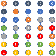
Our approach is highly suitable for optimizing the structure of a QRAM because it essentially functions as a SWAP network. Each node in the ancillary binary tree consists of one qutrit for the address register and one qubit for the data register, denoted as , where and . The value 0 in the address register represents a passive or “wait” mode for the data qubit, while 1 and 2 signify swapping left or right, respectively. Noted that if qutrits are not accessible, qubits could also be used as address registers. Consequently, for a given layer index , the layer can be expressed as . Furthermore, the entire ancillary binary tree, requiring qubits, can be expressed as:
| (26) |
And the initial state of the QRAM binary tree is given by .
Two operations are repeatedly employed in QRAM implementations [29] that are essentially SWAPs. The first is the Internal-SWAP operation. The Internal-SWAP operation alters the state of all address registers within a layer based on the data register of the corresponding node and the address register of its parent node. The Routing operation exchanges the information between the parent node with one of its child nodes based on the status of its address register.
The operation acts on nodes on the -th layer based on the address register of their parent node in the -th layer. In the quantum circuit model, this operation requires controlled-3-2-SWAP gates. For instance, nodes and are modified according to the address register of . Explicitly, the operation can be written as:
| (27) | ||||
where the first qutrit corresponds to the address register of node and the 3-2-SWAP operation is defined specifically for qutrit-qubit nodes, which accomplishes transitions and .
The operation acts on nodes on the -th layer to decide which node in the next layer to land specifically the data on its data register based on its address register. In the quantum circuit model, the routing operation could be decomposed into pairs of SWAP and C-SWAP operations. And each pair has a form like,
| (28) | ||||
Appendix E Detailed Gate Complexity Analysis
In this section, I will summarize the results regarding the gate complexity in the (n, k)-QRAM implementations in the qubit-qubit scheme. The gate complexity analysis focuses on three main phases: the address setting, the uncomputing, and the data fetching.
For address setting and uncomputing, a total of Internal-SWAP and Routing operations are required. During the data fetching process, the number of Routing operations involved can be determined based on the values of and . Specifically, there are Routing operations required, where is defined as:
| (29) |
Alternatively, the expression can be simplified as .
However, it is essential to emphasize that the costs associated with Internal-SWAP and Routing operations can vary across different layers. Specifically, the unidirectional entails pairs of C-SWAP and SWAP operations, whereas bidirectional one requires pairs of two C-SWAP operations. Additionally, necessitates pairs of C-SWAP and SWAP operations. Therefore, in order to accurately assess the gate complexity, it is critical to meticulously count the exact number of Routing and Internal-SWAP operations performed at each layer. This careful consideration allows for a precise evaluation of the overall gate complexity.
The first operation to analyze is the Internal-SWAP during the address setting and uncomputing phase. The total number of Internal-SWAP operations is given by , which can be expressed as for each layer, where ranges from to . In more detail, this is equivalent to , resulting in pairs of C-SWAPS and SWAPS. Additionally, there are two SWAPs specifically for the root.
The next operation to consider is Routing, which is utilized in all three stages of the (n, k)-QRAM implementation. In the address setting and uncomputing phase, the Routing operation is responsible for transferring each address data to layer . This requires the execution of operations, where ranges from to . Each operation involves pairs of operations. Consequently, the total number of C-SWAPs and SWAPs required for Routing in the address setting and uncomputing phase is pairs. In the data fetching phase, the number of pairs of two C-SWAPs needed for Routing depends on the relationship between and . If , it needs , which means . In total, it requires . If , the total sum of pairs would be .
During the address setting and uncomputing phase, as well as the unidirectional Routing operations in the data loading phase, all Routing operations can be simplified using C-iSWAPs and iSWAPs, thanks to the first extension facilitated by our strategy. This simplification is independent of the value of . Consequently, the total number of C-SWAPs and SWAPs saved can be calculated as . On the other hand, the remaining Routing operations are all bidirectional, requiring the second extension. In total, this second extension will save pairs of two C-SWAPs.
When transmitting the data within the (n, k)-QRAM, the number of bidirectional routing operations involved is determined by . As the cost of not doing CZ and CCZ immediately in the QRAM, we require CZ gates for within the QPU, which can be represented as . Additionally, we need to allocate one extra memory cell in the classical memory and calculate the value of . Within the QRAM, an extra CCZ gate is required from the prepared additional memory cell to compensate for the phase before fetching .
In the practical implementation of the (n, k)-QRAM using our decomposing strategy, there are additional resources required. Specifically, the number of CZ gates on the Quantum Processing Unit (QPU) is determined by the sum , and CCZ gates are necessary within the QRAM structure to access the corresponding additional memory cells. These additional resources are essential for the effective operation of the (n, k)-QRAM according to our methodology.
| Extension 1 | Extension 2 | ||||||||
|
|
|
|||||||
|
- | ||||||||
|
- | ||||||||