A superconducting-nanowire single-photon camera with 400,000 pixels
2Department of Physics, University of Colorado, Boulder, Colorado 80309, USA
3Jet Propulsion Laboratory, California Institute of Technology, 4800 Oak Grove Drive, Pasadena, California 91109, USA )
For the last 50 years, superconducting detectors have offered exceptional sensitivity and speed for detecting faint electromagnetic signals in a wide range of applications. These detectors operate at very low temperatures and generate a minimum of excess noise, making them ideal for testing the non-local nature of reality [1, 2], investigating dark matter [3, 4], mapping the early universe [5, 6, 7], and performing quantum computation [8, 9, 10] and communication [11, 12, 13, 14]. Despite their appealing properties, however, there are currently no large-scale superconducting cameras – even the largest demonstrations have never exceeded 20 thousand pixels [15]. This is especially true for one of the most promising detector technologies, the superconducting nanowire single-photon detector (SNSPD) [16, 17, 18]. These detectors have been demonstrated with system detection efficiencies of [19], sub-3-ps timing jitter [20], sensitivity from the ultraviolet (250 nm) [21] to the mid-infrared (10 µm) [22], and dark count rates below counts per second (cps) [3], but despite more than two decades of development they have never achieved an array size larger than a kilopixel [23, 24]. Here, we report on the implementation and characterization of a 400,000 pixel SNSPD camera, a factor of 400 improvement over the previous state-of-the-art. The array spanned an area mm with a µm resolution, reached unity quantum efficiency at wavelengths of and , counted at a rate of cps, and had a dark count rate of cps per detector (corresponding to over the whole array). The imaging area contains no ancillary circuitry and the architecture is scalable well beyond the current demonstration, paving the way for large-format superconducting cameras with 100% fill factors and near-unity detection efficiencies across a vast range of the electromagnetic spectrum.
Most superconducting sensors [25], such as microwave kinetic-inductance detectors (MKIDs) or hot-electron bolometers, produce continuously-valued outputs that lend themselves well to efficient readout schemes such as frequency multiplexing [26]. Superconducting nanowire single-photon detectors, however, are notoriously difficult to multiplex since they produce discrete pulses that are both low-amplitude and broadband. These pulses are typically read out individually using one microwave readout cable per detector, unlike CCD-type sensors which accumulate charge at each pixel and can be serially interrogated with a single readout line. This per-pulse readout process be advantageous when photon-counting as it means there is no read noise, but severely limits the number of detectors that can be read out due to cryogenic thermal load limitations on the readout wiring.
To date, there have been many attempts to devise readout architectures that minimize the number of readout lines running from room temperature electronics to the detector chip. For example, one of the largest architectures to date used a time-of-flight measurement to measure photon position along the length of the detector and required only two readout lines [27]. Unfortunately, since the entire imager was made from a single long nanowire, this architecture is susceptible to fabrication yield issues, as a single discontinuity can compromise the entire imager. Additionally, the large inductance of the long nanowire will inevitably lead to very long reset times and limit the maximum count rate.
In row-column readout architectures, SNSPDs are arranged on an grid [28], enabling readout of pixels using readout lines. The detection event is defined as correlated voltage pulses appearing on both row and column lines within a predefined time window. The row-column readout architecture was used to create the largest SNSPD array to date, a 1,024-pixel imager, but due to diminishing signal-to-noise (SNR) ratio with increasing pixel count, this approach cannot scale to much larger sizes [29]. The thermal row-column scheme overcomes the SNR issue by keeping the row and column pixels electrically isolated and uses the local heat generated during the SNSPD detection process to generate correlated events on row and column channels [30].
More recently, the thermally-coupled imager (TCI) architecture used a combination of thermal coupling to a superconducting bus and time-multiplexing along the readout bus, to achieve kilopixel imaging capability [24]. This scheme used an asymmetric thermal coupling process to transmit pulses on a row or column detector to a readout bus, significantly reducing inter-detector crosstalk and enabling much greater scalability. The SNSPD array demonstrated in this work combines a thermal row-column sensor element with TCI readout in order to achieve its large degree of multiplexing. Additionally, the perpendicular orientation of the two nanowire layers enables polarization-insensitive optical cavity designs.
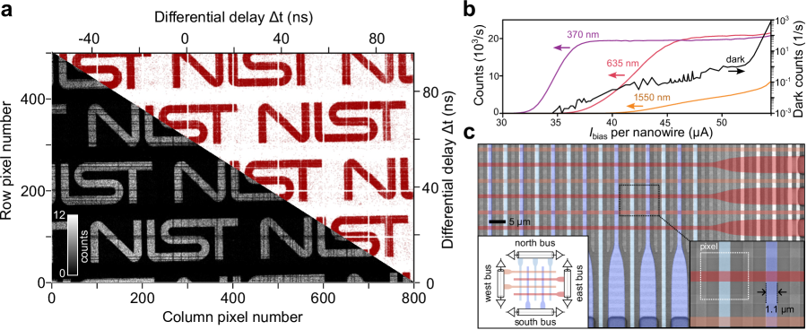
The array, shown in Fig. 1, was comprised of 800 row and 500 column detectors and was operated at a temperature of 0.8 K. The row and column detectors were made by patterning 1.1-µm-wide wires from two independent 4-nm-thick WSi films with a Tc of 3.4 K and kinetic inductance of . Row and column detectors were spaced 5 µm apart and arranged in a grid, giving a resolution of µm as shown in Fig. 1c. There were four buses used for readout, requiring a total of 8 microwave coax lines, and the row and column detectors were interleaved between them as shown in Fig. 1c. Each row or column detector was connected to a resistive thermal coupler, which contained a small heater that is thermally coupled to (but electrically isolated from) the readout bus by a thin, electrically insulating dielectric spacer.
The readout buses were made from the same layer of material as the column detectors and so have the same basic properties. The majority of the bus length had a width of 8 µm that, in combination with the 50-nm-thick SiO2 dielectric spacer and ground plane, formed a microstrip transmission line with approximately 50 impedance. During operation, these sections of the bus contained a relatively low current density and were thus not directly photosensitive, allowing the readout bus to avoid generating false counts from stray photons. Below each heating element, the bus briefly narrowed to a 1.5-µm-wide constriction with high current density, creating a heater-tron like device [31]. The high current density ensured that every time the heater was activated during a detection event, it created a corresponding hotspot on the bus.
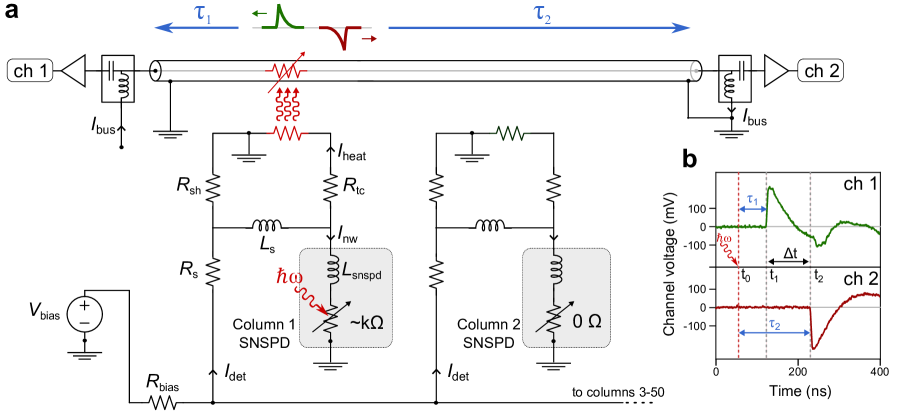
Detectors were grouped into sections of 50 rows or 50 columns, and each section was biased independently. For each section, the bias-current was resistively distributed among the 50 detectors, sharing a common source and ground. Fig. 2 shows the circuit diagram for a single section comprising 50 column SNSPDs. When a photon was absorbed by a detector, a hot-spot formed on the detector with a peak value of a few k. This resistance diverted the bias current out of the detector and into the heating element of the thermal coupler. The resulting phonons generated within the thermal coupler locally destroyed the superconducting state on the readout bus, creating two opposite-polarity voltage pulses that traveled down the readout bus as shown at the top and inset of Fig. 2. Owing to the large kinetic inductance of the bus material, these microwave pulses propagated at 0.36% of (1.10 m/s), allowing relatively short lengths of bus (400 µm) to separate adjacent detectors while maintaining excellent distinguishability.
By measuring the time-difference between the arrival of these pulses at the ends of the buses, one can compute the location of the detection event and the corresponding row or column. As shown in Fig. 2a, for a photon arriving at time , the emitted positive pulse will arrive at the left readout at time , and the negative pulse at . Applying this process to both row and column readout, we were able to precisely identify the location where each photon was absorbed. Given arrival times of and from a column bus and and from a row bus, we calculated the differential time-delays as , . Similarly, the photon time of arrival can be calculated from where is the time-length of the bus. To ensure that these pulses were generated by the same single-photon detection event, we imposed the four-fold coincidence condition that the arrival time of all four pulses were within of each other.
To capture the image shown in Fig. 1a, we patterned a metallic mask on a glass substrate, placed it directly on top of the array, and flood illuminated the entire mask. We then recorded the pulse timings coming out of the readout buses with a timetagger, extracted the four-fold coincidence events, and computed and . No further post processing of the pulse data was performed and no 4-way coincidences were discarded. The raw differential-delay data shown in red corresponds closely to the black and white binned histogram image, excepting the regularly-spaced gaps in the differential-delay data that correspond to extra bus delay between adjacent detector sections.
Fig. 1b shows photon count rate measurements for multiple wavelengths for one of the sections as a function of bias current. As evident from the figure, our detectors have large plateau regions for wavelengths and , indicating unity quantum efficiency over a wide range of bias current. At 370 nm, the wavelength for which this array was targeted, a bias current bias of 40 µA yielded unity quantum efficiency and at this bias current we recorded 5 dark counts over a measurement period of 1,000 s. Since this measurement occurred over a section of 50 detectors, this corresponded to a dark count rate of cps per detector. In a setup that was better shielded optically, this value would likely be even lower, as the dark count curve in Fig. 1b suggests that the source of dark counts at this bias current were likely stray blackbody photons [32].
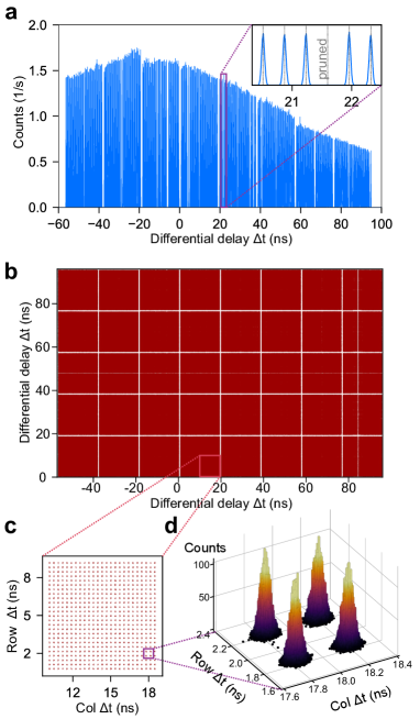
After an initial screening we observed that some detectors were defective, producing anomalously high dark count rates, overwhelming the bus, and obfuscating true counts. To resolve this, we applied a measure-and-prune process to eliminate the faulty detectors. We first determined exactly which detectors were anomalous by flood illuminating the array and collecting 1D histograms for each bus. We then identified any row or column detectors that produced excessive counts and disconnected them by etching through their bias wiring, effectively turning them off. Within a single iteration of this pruning process, we were able to effectively remove all of the defective detectors (58 defective detectors out of 1300), resulting in the smooth Gaussian-spot shape of the histogram shown in Fig. 3a. Identifying the offending detectors was straightforward – the full-width half-max of the peaks was and the separation of the peaks had a median value of , giving a greater than FWHM distinguishability between neighboring rows or columns. We further examined the 2D uniformity of the array by flood illuminating it and examining the output of the buses. As shown in Fig. 3b, the photon counts are tightly clustered in -ps-diameter circles, indicating that the readout process works to accurately position both the photon row and column simultaneously.
One potential area for concern was that detected photons may trigger the detectors but not produce corresponding outputs on the buses, resulting in lost detection events. We characterized this photon-to-bus conversion efficiency with test structures, and found the minimum energy required to create a hotspot on the bus was 8.1 J. In the array, the detection process deposited = 1.2 J of energy on the heater, greatly exceeding the requirements of the thermal coupler. Correspondingly, during operation we observed large operating margins for the detectors and buses, indicating good uniformity and sensitivity of the thermal coupling process. When the detectors were biased between 30-55 µA, any between 15-40 µA produced a photon-to-bus conversion efficiency of approximately unity. We note that while the thermal coupling efficiency was high, an area for improvement will be the increasing the density of the layout for high fill-factors – in the this work, only 13.7 of all photons detected resulted in a four-fold coincidence, due to the relatively large spacing between adjacent detectors.
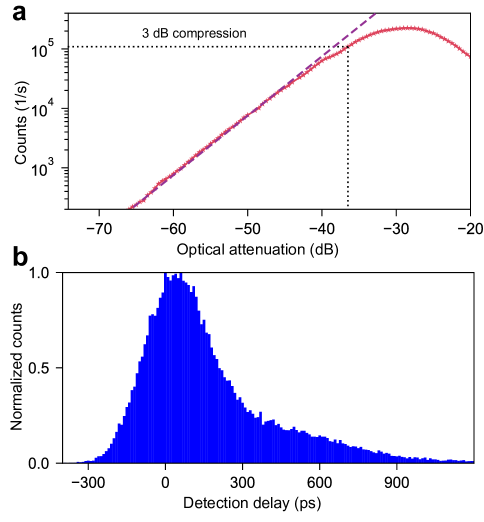
We additionally measured the timing performance of the array. Fig. 4a shows the count rate from one of the 50-detector sections versus optical attenuation measured at and with the detectors biased at 45 µA per detector. We observed that the photon count rate was proportional to the photon flux, indicating the array was operating in the single-photon regime [16, 33]. The count rate was limited primarily by the speed of the bus – after detection, the current in the bus dropped to zero for a period of time , and any other photon detections during this time would be lost. For our device this dead time was . Similar to single-pixel SNSPDs, once count-rates approached , photons could still be lost due to blocking loss as evidenced by the 3 dB compression point at 1.09 cps. To increase the maximum readout rate, additional buses may be added trivially. For a fixed array size, increasing the total number of buses by a factor of leads to a -fold increase in the maximum readout rate per bus and thus a -fold increase in the maximum readout rate of the entire array.
Fig. 4b shows the timing jitter of one of the array sections. To obtain this data a single section was biased and illuminated with a mode-locked laser with optical pulse width. The distribution of detection delays had the FWHM of and standard deviation of . This relatively large jitter can be primarily attributed to the longitudinal geometric jitter of our long detectors, and could be significantly reduced by converting to a differential-style readout [34].
In this work, we demonstrated the largest superconducting photon-counting camera to date by a factor of 20, using an efficient, time-resolved architecture that is both scalable and tolerant of fabrication defects. The architecture allows for the imaging area to contain only detectors, allowing future arrays to reach 100% fill factors with high system detection effiencies. While the work here demonstrated classical imaging at the single-photon level, we expect future large-format implementations to greatly enable applications in quantum imaging[35] such as sub-Rayleigh super-resolution imaging[36] or sub-shot-noise imaging[37]. These applications typically require the detection of quantum correlations in both time and space, and depend heavily on high efficiencies and low background noise.
Methods
The chip was fabricated with 6 layers: two WSi detectors layers, two Nb wiring layers, a resistor layer, and a dielectric spacer layer. First, we sputtered a thin () WSi film on a Si wafer with of thermal oxide. The film was in-situ capped with of aSi to avoid oxidation. Then column detectors, series inductors and the readout bus were patterned using SPR660 and optical lithography with an i-line () stepper. Finally these patterns were etched with an inductively-coupled plasma (ICP) etcher using an AR:SF6 etch. Next, a liftoff pattern was created using optical lithography and thick Nb wires with of PdAu capping were sputtered to create a low inductance bottom Nb wiring layer.
At this point, it is important to planarize the surface before depositing row detectors. In our tests, it was observed that if this planarization step is skipped, the topography of the column detectors results in a step-like edges on the row detectors which reduces the critical current of row detectors, degrading their performance. The planarization can be achieved by using a dilute divinylsiloxane-benzocyclobutene (DVS-BCB) polymer. This BCB polymer was applied to the wafer, and spun dry at . The wafer was later baked at in a nitrogen furnace for 60 min, to cure the BCB. Later, of SiO2 was sputtered on the wafer with of amorphous silicon sputtered in-situ as a capping layer. Finally, the wafer was patterned and etched with a CHF3 and O2 chemistry to create vias through the dielectric layer. The PdAu deposited on the bottom Nb wiring layer acts as a non-oxidizing etch stop, allowing us to overetch and create µm vias.
Next, of WSi film was sputtered again, patterned and etched to produce row detectors and the heaters on the thermal coupler. Later, of PdAu was sputtered with a liftoff process to create all of the resistors needed for the device operation (see Fig. 2). Finally, 200 nm of Nb was sputtered and patterned with a liftoff process to create the top Nb wiring layer and the GND plane for readout buses. of Ti was used as an adhesion layer for the Nb and PdAu layers.
After this we performed the final etch to disconnect the ground from the readout bus, which was intentionally left connected to the ground plane. Skipping this step usually causes antenna-like RF-pickup, leading to damage of the readout bus in our devices. To improve the yield and reproducibility of lithographically defined patterns, the detectors were designed as images containing 10 detectors, and the stepper was used to repeat this pattern forming the full array. The readout circuits and readout bus were designed to connect to 50 detectors each. The overall pattern was generated by rotating the wafer inside the stepper and repeating these images, hence both column and row detectors and their readout circuitry are produced with the same reticles.
The chip was fabricated as a array, and during testing we identified a uniform section of 800 column detectors and 500 row detectors, which we designated as the active detection area. This demonstrates the flexibility of the architecture, since the unbiased sections of the array do not waste any bandwidth on the readout buses. The same technique can be straightforwardly applied to allow selection of an active area on-the-fly.
Circuit parameter values
In this implementation, the values for the circuit elements were optimized using test structures as well as SPICE simulations. The section biasing resistor was 1000 , the detector biasing resistor Rs was 80 , the shunting resistor was 16 , the thermal coupler series resistor was 16 , the series inductor was , and the inductance of the SNSPD was . The biasing resistor Rs needed to be sufficiently large to ensure that current was distributed uniformly to each detector – if made too small, parasitic resistances in the wiring or vias can cause uneven distribution. However, larger values also contribute to the static power consumption of the array and so its value cannot be too large. was chosen to be relatively small, as it allows the current to be shunted to ground after a detector clicked. By choosing an appropriately small value, the detectors are sufficiently shunted such that latching is impossible, simplifying the operation of the array. Additionally, a small value of guarantees that voltages generated during the detection process are shunted before they reach the communal bias line, minimizing crosstalk between neighboring detectors in a section.
A large value of serves to both minimize crosstalk voltages on the bias line during detection, and acts as an energy reservoir with which to power the heating element on the thermal coupler. Too-large values, however, result in wasted space on the chip as well as generate excess heating of the bus that can negatively affect reset times. While smaller values would be preferred to minimize geometric jitter and reset time in the detectors, for this design we required least -long detectors to span the imaging area.
1 Data availability
2 Code availability
3 Acknowledgements
The U.S. Government is authorized to reproduce and distribute reprints for governmental purposes notwithstanding any copyright annotation thereon. Part of this research was performed at the Jet Propulsion Laboratory, California Institute of Technology, under contract with NASA (Contract No. 80NM0018D0004). A.N.M. was supported in part by NASA APRA via Grant No. NNH17ZDA001N. Support for this work was provided in part by the DARPA DSO Invisible Headlights program. Certain equipment, instruments, software, or materials, commercial or non-commercial, are identified in this paper in order to specify the experimental procedure adequately. Such identification is not intended to imply recommendation or endorsement of any product or service by NIST, nor is it intended to imply that the materials or equipment identified are necessarily the best available for the purpose. This research was funded by NIST (https://ror.org/05xpvk416), University of Colorado Boulder (https://ror.org/02ttsq026), and the Jet Propulsion Laboratory (https://ror.org/027k65916).
4 Author contributions
ANM, BK, and BGO conceptualized these experiments. Fabrication of devices was done by BGO. Measurements were performed by BGO, DSR and ANM. Analysis and interpretation of the data was done by BGO, SWN, MDS, BK, and JA. ANM directed and supervised this work. BGO and ANM prepared the manuscript with input from all co-authors.
References
- [1] Marissa Giustina et al. “Significant-Loophole-Free Test of Bell’s Theorem with Entangled Photons” In Physical Review Letters 115.25, 2015, pp. 250401 DOI: 10.1103/PhysRevLett.115.250401
- [2] Lynden K. Shalm et al. “Strong Loophole-Free Test of Local Realism” In Phys. Rev. Lett. 115 American Physical Society, 2015, pp. 250402 DOI: 10.1103/PhysRevLett.115.250402
- [3] Jeff Chiles et al. “New Constraints on Dark Photon Dark Matter with Superconducting Nanowire Detectors in an Optical Haloscope” In Phys. Rev. Lett. 128 American Physical Society, 2022, pp. 231802 DOI: 10.1103/PhysRevLett.128.231802
- [4] Akash V. Dixit et al. “Searching for Dark Matter with a Superconducting Qubit” In Physical Review Letters 126.14, 2021, pp. 141302 DOI: 10.1103/PhysRevLett.126.141302
- [5] Dominik A Riechers et al. “A dust-obscured massive maximum-starburst galaxy at a redshift of 6.34” In Nature 496.7445, 2013, pp. 329–333
- [6] de Bernardis P et al. “A flat Universe from high-resolution maps of the cosmic microwave background radiation” In Nature 404.6781, 2000, pp. 955–959
- [7] C. Nones et al. “High-impedance NbSi TES sensors for studying the cosmic microwave background radiation” In Astronomy & Astrophysics 548, 2012, pp. A17 DOI: 10.1051/0004-6361/201218834
- [8] J M Arrazola et al. “Quantum circuits with many photons on a programmable nanophotonic chip” In Nature 591.7848, 2021, pp. 54–60
- [9] S.. Todaro et al. “State Readout of a Trapped Ion Qubit Using a Trap-Integrated Superconducting Photon Detector” In Physical Review Letters 126.1, 2021, pp. 010501 DOI: 10.1103/PhysRevLett.126.010501
- [10] Lars S. Madsen et al. “Quantum computational advantage with a programmable photonic processor” In Nature 606.7912, 2022, pp. 75–81 DOI: 10.1038/s41586-022-04725-x
- [11] Alberto Boaron et al. “Secure Quantum Key Distribution over 421 km of Optical Fiber” In Phys. Rev. Lett. 121, 2018, pp. 190502
- [12] Shuang Wang et al. “Twin-field quantum key distribution over 830-km fibre” In Nat. Photonics 16.2 Nature Publishing Group, 2022, pp. 154–161
- [13] Fadri Grünenfelder et al. “Fast single-photon detectors and real-time key distillation enable high secret-key-rate quantum key distribution systems” In Nat. Photonics 17.5, 2023, pp. 422–426
- [14] Wei Li et al. “High-rate quantum key distribution exceeding 110 Mb s–1” In Nat. Photonics 17.5 Nature Publishing Group, 2023, pp. 416–421
- [15] Alexander B. Walter et al. “The MKID Exoplanet Camera for Subaru SCExAO” In Publications of the Astronomical Society of the Pacific 132.1018, 2020, pp. 125005 DOI: 10.1088/1538-3873/abc60f
- [16] G.. Gol’tsman et al. “Picosecond superconducting single-photon optical detector” In Applied Physics Letters 79.6, 2001, pp. 705–707 DOI: 10.1063/1.1388868
- [17] Robert H Hadfield “Single-photon detectors for optical quantum information applications” In Nat. Photonics 3.12 Nature Publishing Group, 2009, pp. 696–705
- [18] F Marsili et al. “Detecting single infrared photons with 93 % system efficiency” Nature Publishing Group, 2013
- [19] Dileep V. Reddy et al. “Superconducting nanowire single-photon detectors with 98 system detection efficiency at 1550 nm” In Optica 7.12 Optica Publishing Group, 2020, pp. 1649–1653 DOI: 10.1364/OPTICA.400751
- [20] Boris Korzh et al. “Demonstration of sub-3 ps temporal resolution with a superconducting nanowire single-photon detector” In Nature Photonics 14, 2020, pp. 250–255 DOI: https://doi.org/10.1038/s41566-020-0589-x
- [21] E E Wollman et al. “UV superconducting nanowire single-photon detectors with high efficiency, low noise, and 4 K operating temperature” In Opt. Express 25.22, 2017, pp. 26792
- [22] V B Verma et al. “Single-photon detection in the mid-infrared up to 10 m wavelength using tungsten silicide superconducting nanowire detectors” In APL Photonics 6.5 AIP Publishing, LLC, 2021, pp. 056101
- [23] Emma E Wollman et al. “A kilopixel array of superconducting nanowire single-photon detectors” In Opt. Express 27.24, 2019, pp. 35279–35289
- [24] A.. McCaughan et al. “The thermally coupled imager: A scalable readout architecture for superconducting nanowire single photon detectors” In Applied Physics Letters 121.10, 2022, pp. 102602 DOI: 10.1063/5.0102154
- [25] Dmitry V. Morozov, Alessandro Casaburi and Robert H. Hadfield “Superconducting photon detectors” In Contemporary Physics 62.2 Taylor & Francis, 2021, pp. 69–91 DOI: 10.1080/00107514.2022.2043596
- [26] Peter K..K. Day et al. “A broadband superconducting detector suitable for use in large arrays” In Nature 425.6960 Nature Publishing Group, 2003, pp. 817–821 DOI: 10.1038/nature02037
- [27] Qing-Yuan Zhao et al. “Single-photon imager based on a superconducting nanowire delay line” In Nature Photonics 11, 2017, pp. 247–251 DOI: https://doi.org/10.1038/nphoton.2017.35
- [28] V.. Verma et al. “A four-pixel single-photon pulse-position array fabricated from WSi superconducting nanowire single-photon detectors” In Applied Physics Letters 104.5, 2014, pp. 051115 DOI: 10.1063/1.4864075
- [29] Emma E. Wollman et al. “Kilopixel array of superconducting nanowire single-photon detectors” In Opt. Express 27.24 Optica Publishing Group, 2019, pp. 35279–35289 DOI: 10.1364/OE.27.035279
- [30] Jason P. Allmaras et al. “Demonstration of a Thermally Coupled Row-Column SNSPD Imaging Array” PMID: 32091221 In Nano Letters 20.3, 2020, pp. 2163–2168 DOI: 10.1021/acs.nanolett.0c00246
- [31] A.. McCaughan et al. “A superconducting thermal switch with ultrahigh impedance for interfacing superconductors to semiconductors” In Nature Electronics 2.10, 2019, pp. 451–456 DOI: 10.1038/s41928-019-0300-8
- [32] T. Yamashita et al. “Origin of intrinsic dark count in superconducting nanowire single-photon detectors” 161105 In Applied Physics Letters 99.16, 2011 DOI: 10.1063/1.3652908
- [33] Ioana Craiciu et al. “High-speed detection of 1550 nm single photons with superconducting nanowire detectors” In Optica 10.2 Optica Publishing Group, 2023, pp. 183–190 DOI: 10.1364/OPTICA.478960
- [34] Marco Colangelo et al. “Impedance-Matched Differential Superconducting Nanowire Detectors” In Phys. Rev. Appl. 19 American Physical Society, 2023, pp. 044093 DOI: 10.1103/PhysRevApplied.19.044093
- [35] Paul-Antoine Moreau, Ermes Toninelli, Thomas Gregory and Miles J. Padgett “Imaging with quantum states of light” In Nature Reviews Physics 1.6, 2019, pp. 367–380 DOI: 10.1038/s42254-019-0056-0
- [36] Vittorio Giovannetti, Seth Lloyd, Lorenzo Maccone and Jeffrey H. Shapiro “Sub-Rayleigh-diffraction-bound quantum imaging” In Physical Review A 79.1, 2009, pp. 013827 DOI: 10.1103/PhysRevA.79.013827
- [37] G. Brida, M. Genovese and I. Ruo Berchera “Experimental realization of sub-shot-noise quantum imaging” In Nature Photonics 4.4, 2010, pp. 227–230 DOI: 10.1038/nphoton.2010.29