figuret
Optical properties of ScN layers grown on Al2O3(0001) by plasma-assisted molecular beam epitaxy
Abstract
An accurate knowledge of the optical constants (refractive index and extinction coefficient ) of ScN is crucial for understanding the optical properties of this binary nitride semiconductor as well as for its use in optoelectronic applications. Using spectroscopic ellipsometry in a spectral range from far infrared to far ultraviolet (0.045–8.5 eV), we determine and of ScN layers grown on Al2O3(0001) substrates by plasma-assisted molecular beam epitaxy. Fits of ellipsometry data return the energies of four oscillators representing critical points in the band structure of ScN, namely, 2.03, 3.89, 5.33, and 6.95 eV. As the infrared range is dominated by free carriers, the vibrational properties of the layers are examined by Raman spectroscopy. Despite the rocksalt structure of ScN, several first-order phonon modes are observed, suggesting a high density of point defects consistent with the high electron density deduced from Hall measurements. Finally, photoluminescence measurements reveal an emission band slightly above the lowest direct bandgap. We attribute the redshift of the peak emission energy from 2.3 to 2.2 eV with increasing layer thickness to a reduction of the O concentration in the layers.
The rocksalt semiconductor ScN has been first synthesized more than five decades ago.[1, 2, 3] More recently, ScN has attracted much interest in conjunction with the conventional group-III nitrides, i.e., GaN and AlN. In particular, the ternary alloy (Sc,Al)N holds great potential for applications in surface acoustic wave devices,[4, 5] field-effect transistors,[6, 7, 8] and as novel ferroelectric material.[9, 10] Recently, high-quality ScN has been grown using plasma-assisted molecular beam epitaxy (PAMBE)[11, 12] and hydride vapor phase epitaxy,[13] enabling new applications of pure ScN. In fact, ScN has been theoretically and experimentally proposed for electronic,[14] thermoelectric[15] and infrared optoelectronic applications.[16]
In terms of its electronic properties, both experimental and theoretical studies have shown that ScN has an indirect gap at about 0.8–0.9 eV,[17, 18, 19] a direct gap at 1.91–3.1 eV at the point,[3, 20, 21, 22, 23, 18, 24, 25, 26, 17, 27, 13, 11, 15] and a direct gap of 3.58–3.75 eV at the point in the band structure of ScN.[18, 25, 19] Room-temperature photoluminescence measurements of ScN show an emission band at about 2.2–2.3 eV corresponding to the lowest direct gap.[27, 11, 28] Compared to GaN and AlN, the optical constants (refractive index and extinction coefficient ) of ScN are less well known, with having been most commonly extracted from transmittance[3, 22, 23, 24, 25] and reflectance measurements.[22, 23, 25, 18] While there is a good agreement between extracted from reflectance data for photon energies of 1–2 eV and density-functional-theory (DFT),[18] it is important to extend these measurements to the spectral range where ScN starts to absorb strongly, i.e., above its lowest direct band gap.
Spectroscopic ellipsometry (SE) is a technique ideally suited for this task because it allows us to derive the complex refractive index or dielectric function from a single measurement, without the need of an intensity reference, or the Kramers–Kronig transformation required for transmittance or reflectance data alone. SE is the method of choice for an accurate determination of both and over a wide spectral range, and is thus frequently used to extract reliable information on phononic and electronic transitions that can be compared with the predictions of DFT. In this way, SE provides important insights into the phonon and electron dispersion relationships of the material under investigation.[29, 30] Consequently, SE was employed by several groups to determine the dielectric function of ScN, but only in a limited spectral range.[22, 31, 16, 27] Most importantly, a critical comparison of the dielectric function acquired over a wide spectral range with the predictions of modern DFT calculations has yet to be performed.
In this letter, we determine the dielectric function of ScN layers grown on Al2O3(0001) substrates by PAMBE using SE over a spectral range of 0.045–8.5 eV. The data are fit with an parametric model to accurately determine the energies of the critical points in the band structure of ScN, and compared to the results of recent DFT calculations utilizing improved exchange correlation functionals. Additional information on the phononic properties is obtained by Raman spectroscopy. Finally, photoluminescence spectroscopy is used to shed light on the origin of the high electron density in the layers.
ScN layers are grown by PAMBE on as-received Al2O3(0001) substrates (either on quarters or full 2-inch wafers). Prior to ScN growth, the substrates were outgassed for two hours at 500 °C in a load-lock chamber attached to the MBE system. The MBE growth chamber is equipped with a high-temperature effusion cell to provide Sc metal (99.999 % pure Sc). A Veeco UNI-Bulb radio-frequency plasma source is used for the supply of active nitrogen (N∗). The N∗ flux is calculated from the thickness of a GaN layer grown under Ga-rich conditions, and thus with a growth rate limited by the N∗ flux. The Sc flux is obtained from the thickness of thin ScN calibration layers (40 nm) measured by x-ray reflectivity. The growth temperature as measured by a thermocouple is set to 700 °C. The ScN layers are grown with thicknesses ranging from 8 to 250 nm under N∗-rich conditions. Information about the structural properties, lattice constants and surface morphology of the layers is provided in Figs. S1–S4 in the Supplementary Material.
SE measurements are carried out at room temperature for two incident angles of 65 and 75° (with respect to the normal of the sample) using two Woollam ellipsometers, which have a combined spectral range from the far infrared (IR) to the far ultraviolet, specifically, 0.045–8.5 eV. The optical constants of the ScN layers are determined by fitting the ellipsometry data with a parametric model that represents the electronic and phononic contributions as a collection of oscillators. Raman and photoluminescence (PL) spectra of the layers are recorded at room temperature using a Horiba LabRAM HR Evolution. The samples are excited with a 405-nm laser diode focused onto their surface with a spot diameter of about 2 m (power density 25 kW/cm2).
In ellipsometry, the amplitude ratio and the phase shift between light polarized parallel and perpendicular to the plane of incidence are measured.[32] Because these measured ellipsometry parameters depend on the thickness and optical constants of each layer of a structure, we develop a model that varies the thicknesses and optical constants of each layer, and change the model parameters to obtain a best fit for the experimental spectra. While the optical constants in the transparent range are well represented by a Cauchy relationship, they are modeled in the opaque range by a collection of oscillators, each representing a resonance associated with an electronic transition.[33]
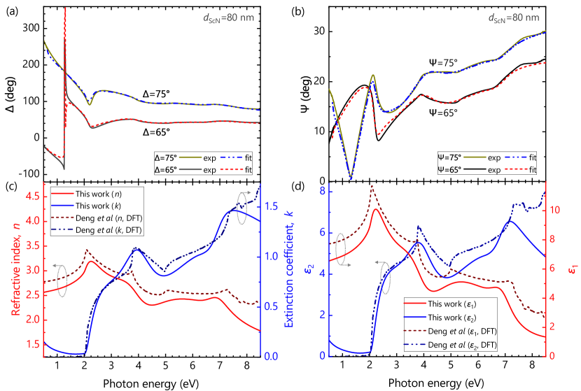
Figures 1(a) and 1(b) show and spectra for the entire spectral range measured for the 80-nm-thick ScN layer, respectively. Spectra in the IR range between 0.045 and 0.15 eV are shown in Fig. S5 of the Supplementary Material. Furthermore, Fig. S6 of the Supplementary Material presents a comparison with a 250-nm-thick ScN layer and experimental data taken from Ref. 16. To fit the experimental spectra, we develop a three-layer model consisting of the Al2O3 substrate, the ScN layer and a top layer accounting for surface roughness modeled by a Bruggemann effective medium approximation.[34] The dielectric function of Al2O3 was obtained by measuring a pristine Al2O3(0001) substrate, and is found to compare well with results reported in the literature.[35, 36] In order to determine the thicknesses of the ScN and the roughness layers, we use a narrow spectral range between 1 and 2 eV of the measured spectra. Because ScN is essentially transparent in this range, its optical constants are represented by a Cauchy relationship (with a near-zero -value).[33] As the number of fitting parameters is low, this method allows us to obtain unique values for the thicknesses of the ScN (81.5 nm) and the roughness layer (8.8 nm).
Following the determination of the thicknesses of the layers and in the transparent range, we perform a simultaneous wavelength-by-wavelength fit of and for the entire spectral range. This procedure may, in general, produce and values that do not obey the Kramers-Kronig relation. In the present work, the and values obtained from the wavelength-by-wavelength fit are used to construct Kramers-Kronig consistent-oscillators that represent the actual optical constants of ScN.[33] To fit the ellipsometry data, we use a five-oscillator model (see Fig. S7 in the Supplemental Material), where four oscillators represent band-to-band electronic transitions (Tauc-Lorentz oscillators[37]) associated with the critical points (i.e., high-symmetry points) of the band structure of ScN and the fifth represents free electron absorption (i.e., a Drude oscillator[33]). A slow variation of the baseline is accounted for by two additional oscillators below and above the experimental spectral range.
Figure 1 shows the results of the fits in terms of (c) the complex refractive index and (d) the complex dielectric function . Each panel also depicts the corresponding theoretical predictions obtained from density functional calculations using the Heyd-Scuseria-Ernzerhof (HSE06) hybrid exchange correlation functional.[18] As commonly observed, the experimental features are broadened compared to the theoretical ones, reflecting a certain degree of disorder in the material. In the present case, the high density of point defects in the ScN layer is the primary source for this disorder as discussed in more detail below. However, the overall agreement of experiment and theory is very satisfactory, except for a notable deviation at energies higher than 7.5 eV. At these energies, the penetration depth of light is reduced to about 10 nm, comparable to the peak-to-valley roughness of the layer under investigation. Hence, the optical constants measured in this spectral range are those of an effective medium rather than being representative for bulk ScN.
The lowest oscillator at 2.03 eV corresponds to the lowest energy direct transition at the point. The other three oscillators are associated with direct transitions that occur at the point between the degenerate heavy- and light-hole bands and the first, second and third conduction bands, and have energies of 3.89, 5.33, and 6.95 eV, respectively. Interestingly, the oscillator strength of the transition with an energy of 5.33 eV is considerably higher than that of the other two transitions (see Fig. S7 in the Supplemental Material), indicating that it may encompass more than a single transition. Upon closer scrutiny of the band structure of ScN,[18] we notice that the degeneracy between the heavy- and light-hole bands is lifted at the point. The energy difference between the light-hole band and the conduction band at the point is basically equal to the one between the valence band and the second conduction band at the point. The oscillator at 5.33 eV thus represents a superposition of two direct transitions.
The values of or in the spectral range below 2 eV deviate significantly from the theoretical values [Figs. 1(c)–1(d)], which are obtained assuming an intrinsic semiconductor devoid of any doping.[18] In reality, ScN layers are invariably degenerately -type doped, inducing a significant free-carrier absorption in the IR spectral range. This contribution to the dielectric function is taken into account in our model by a Drude oscillator, which governs its behavior in the transparent range below 2 eV. The best fit of the SE data, assuming an effective electron mass of (), return an electron density of 1.11020 cm-3 and a mobility of 3.4 cm2V-1s-1, consistent with Hall-effect measurements on this layer (performed in the van der Pauw configuration at room temperature).
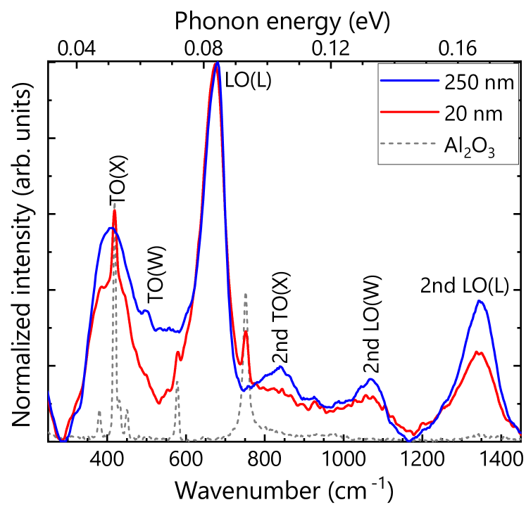
Previous reports have indicated that the transverse optical (TO)[38, 39, 16] and the longitudinal optical (LO)[16] phonon modes in ScN are located at 360–365 cm-1 and 685 cm-1, respectively, or 0.045 and 0.085 eV, which is within the range we have measured in the IR range (see Fig. S5 in the Supplemental Material). However, the strong free-carrier absorption, as well as the strong phonon resonances of the Al2O3 substrate,[40] dominate the optical response for very low photon energies. In fact, the Drude oscillator is perfectly adequate for fitting the experimental data as seen in Fig. S7 in the Supplemental Material, with no need to include additional oscillators to account for the phonon modes of ScN.
We thus investigated the vibrational properties of the ScN layers by Raman spectroscopy. Generally, for materials with rocksalt structure, first-order Raman scattering by optical phonon modes is forbidden. Point defects such as vacancies and substitutional impurities may break this symmetry, but also structural defects such as twin boundaries.[41, 38, 42] In the Raman spectrum shown in Fig. 2, some phonon modes from Al2O3 (e.g., at 418 and 750 cm-1) are detected for the 20-nm-thick layer, but are no longer present once the layer thickness exceeds the penetration depth of the exciting laser. Hence, the remaining phonon modes can be assigned to ScN. Several first-order modes at the , and points of the phonon band structure of ScN are observed, which we assign to the TO(X) at 420 cm-1, TO(W) at 500 cm-1, LO(W) at 535 cm-1 and LO(L) mode at () cm-1, consistent with experiments conducted on bulk ScN crystals,[38] untwinned ScN layers,[11] as well as with theory.[43, 39] The prominence of zone-boundary modes, particularly the LO(L), has been discussed in detail by Paudel and Lambrecht.[39]
The LO(L) spectral position is independent of the layer thickness, indicating that all of our layers are essentially fully relaxed as also suggested by x-ray diffractometry revealing a very small residual strain (see Fig. S3 in the Supplemental Material). This virtually full plastic relaxation is expected because the lattice mismatch between ScN(111) and Al2O3(0001) is huge [16% according to the relaxed lattice constants of ScN[44, 45, 38] and Al2O3(0001)[46]].
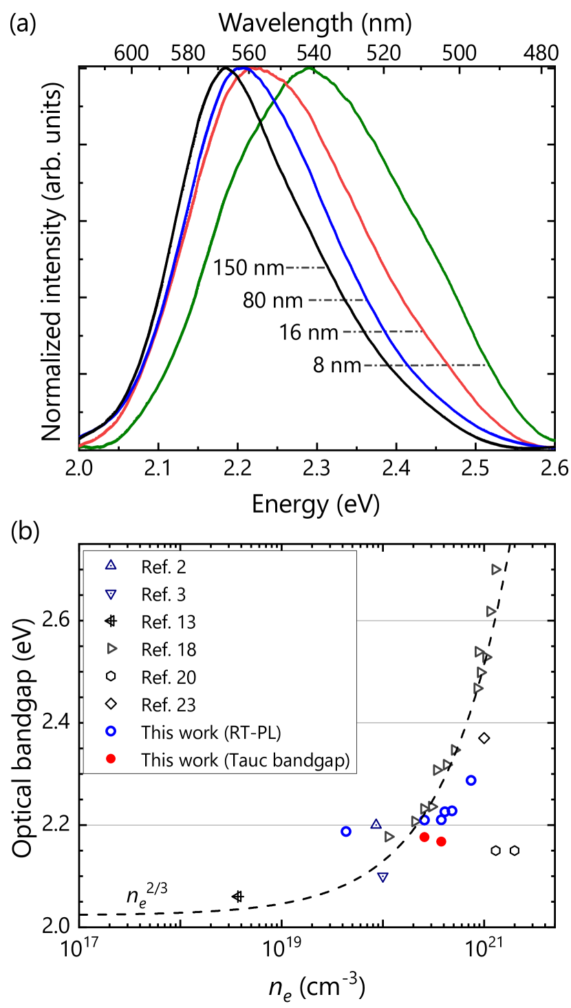
Figure 3(a) shows the PL spectra of the ScN layers under investigation. Analogously to previous reports in the literature,[27, 11] the PL spectra of our ScN layers exhibit a broad band close to the lowest direct band-gap at the point. Direct-gap PL of indirect semiconductors has been observed before, and was found to be much enhanced for heavily doped layers.[47, 48] This emission band stems, in general, from the recombination of majority carriers with nonthermalized minority carriers at the same point of the Brillouin zone. For the particular case of ScN, the commonly reported electron densities in excess of 1020 cm-3 result in the Fermi level entering the conduction band and a corresponding band filling.[18, 49] The degenerate doping thus facilitates the recombination of electrons populating the conduction-band minimum with hot photogenerated holes in the uppermost valence-band at the point.
The emission energy of the spectra depicted in Fig. 3(a) is seen to monotonically decrease from 2.3 to 2.2 eV with increasing layer thickness, very similar to the observation reported in Ref. 11. Furthermore, the width of the band decreases notably (see Fig. S8 in the Supplemental Material for details). While the layers experience a reduction in compressive strain from 0.3 to 0.1% (see Fig. S3 of the Supplementary Material), the effect of the decreasing strain on the transition energy is much smaller than that observed. At the same time, Hall-effect measurements reveal a decrease in electron density from 7.41020 cm-3 to 4.31019 cm-3 with increasing layer thickness with a corresponding reduction in band filling.
Figure 3(b) shows the dependence of the optical band gap of ScN on as reported in the literature and observed by us using spectroscopic ellipsometry. The optical band gap is obtained by Tauc plots[20] with the absorption coefficients either derived from transmittance and reflectance measurements or, in our case, directly obtained from the extinction coefficient . The strong blueshift observed for cm-3 is due to band filling (Burstein-Moss effect) and follows the theoretically expected dependence.[18, 49] While this shift would not be observable in emission for an ideal crystal, the presence of a high density of ionized donors induces disorder that relaxes conservation, allowing the recombination of electrons and holes occupying higher energy states with different vectors.[50, 51] For comparison, Fig. 3(b) also shows the peak energy of the emission bands depicted in Fig. 3(a). Note, however, that this comparison is not straightforward: while absorption sets in at the Fermi energy, the PL lineshape depends on occupation, and is here complicated by the very large high-energy broadening originating from the highly nonthermal hole distribution.[47] The peak energy thus does not, in general, correspond to the Fermi energy.[50] Still, the PL peak energies are in overall agreement with the optical gap, and provide a very convenient and direct means to obtain information about the degeneracy of ScN layers.
To summarize and conclude, we have used SE in a spectral range from 0.045 to 8.5 eV to determine the optical constants of ScN layers grown on Al2O3 substrates using PAMBE. Parametric fits of the SE data return the energies of the four lowest direct band-to-band transitions of 2.03, 3.89, 5.33, and 6.95 eV, corresponding to the high-symmetry critical points in the band structure of ScN. In the infrared range, free carrier absorption due to the high electron density dominates the dielectric function, and we have thus used Raman spectroscopy to examine the vibrational properties of the layers. Strong first-order modes are observed, which indicate the existence of defects in the layers breaking the symmetry of the rocksalt structure. Likewise, the shape and position of the PL band observed in the vicinity of the lowest direct gap is governed by defects relaxing conservation and allowing transitions indirect in space. The reduction of the electron density with increasing layer thickness suggests that O impurities stemming from the substrate are a likely candidate for these defects. A similar conclusion has been reached in Ref. 11 for ScN growth on Sc2O3 buffer layers.
See supplementary material for (1) symmetric – XRD scans of the ScN layers; (2) azimuthal scans performed in skew symmetry of the ScN 220 and Al2O3 112̄3 reflections; (3) evolution of the lattice constant with layer thickness, including literature values; (4) atomic force topographs of layers with different thickness; (5) measured and fitted and spectra in the range of 0.045–0.15 eV and the corresponding real and imaginary parts of the complex refractive index and the complex dielectric function ; (6) comparison of the real and imaginary parts of the complex refractive index and the complex dielectric function obtained for the 80- and 250-nm-thick ScN layers, compared to the results obtained by Maurya et al. [16]; (7) Drude and Tauc-Lorentz oscillators of the 80-nm-thick ScN layer; (8) peak energy and full-width at half-maximum of PL spectra of the layers as a function of electron density.
We thank Carsten Stemmler for expert technical assistance with the MBE system.
References
- Sclar [1964] N. Sclar, “Properties of rare-earth nitrides,” J. Appl. Phys. 35, 1534–1538 (1964).
- Dismukes et al. [1970] J. P. Dismukes, W. M. Yim, J. J. Tietjen, and R. E. Novak, “Vapor deposition of semiconducting mononitrides of scandium, yttrium, and the rare-earth elements,” RCA Rev. 31, 680–691 (1970).
- Dismukes, Yim, and Ban [1972] J. P. Dismukes, W. M. Yim, and V. S. Ban, “Epitaxial growth and properties of semiconducting ScN,” J. Cryst. Growth 13-14, 365–370 (1972).
- Akiyama et al. [2009] M. Akiyama, T. Kamohara, K. Kano, A. Teshigahara, Y. Takeuchi, and N. Kawahara, “Enhancement of piezoelectric response in scandium aluminum nitride alloy thin films prepared by dual reactive cosputtering,” Adv. Mater. 21, 593–596 (2009).
- Hashimoto et al. [2013] K.-y. Hashimoto, S. Sato, A. Teshigahara, T. Nakamura, and K. Kano, “High-performance surface acoustic wave resonators in the 1 to 3 GHz range using a ScAlN/6H-SiC structure,” IEEE Trans. Ultrason. Ferroelectr. Freq. Control 60, 637–642 (2013).
- Hardy et al. [2017] M. T. Hardy, B. P. Downey, N. Nepal, D. F. Storm, D. S. Katzer, and D. J. Meyer, “Epitaxial ScAlN grown by molecular beam epitaxy on GaN and SiC substrates,” Appl. Phys. Lett. 110, 162104 (2017).
- Wang et al. [2021] P. Wang, D. Wang, B. Wang, S. Mohanty, S. Diez, Y. Wu, Y. Sun, E. Ahmadi, and Z. Mi, “N-polar ScAlN and HEMTs grown by molecular beam epitaxy,” Appl. Phys. Lett. 119, 082101 (2021).
- Dinh et al. [2023] D. V. Dinh, J. Lähnemann, L. Geelhaar, and O. Brandt, “Lattice parameters of ScxAl1-xN layers grown on GaN(0001) by plasma-assisted molecular beam epitaxy,” Appl. Phys. Lett. 122, 152103 (2023).
- Wang et al. [2022] P. Wang, D. Wang, S. Mondal, and Z. Mi, “Ferroelectric N-polar ScAlN/GaN heterostructures grown by molecular beam epitaxy,” Appl. Phys. Lett. 121, 023501 (2022).
- Wang et al. [2023] D. Wang, P. Wang, S. Mondal, M. Hu, D. Wang, Y. Wu, T. Ma, and Z. Mi, “Thickness scaling down to 5 nm of ferroelectric ScAlN on CMOS compatible molybdenum grown by molecular beam epitaxy,” Appl. Phys. Lett. 122, 052101 (2023).
- Lupina et al. [2015] L. Lupina, M. H. Zoellner, T. Niermann, B. Dietrich, G. Capellini, S. B. Thapa, M. Haeberlen, M. Lehmann, P. Storck, and T. Schroeder, “Zero lattice mismatch and twin-free single crystalline ScN buffer layers for GaN growth on silicon,” Appl. Phys. Lett. 107, 201907 (2015).
- Casamento et al. [2019] J. Casamento, J. Wright, R. Chaudhuri, H. G. Xing, and D. Jena, “Molecular beam epitaxial growth of scandium nitride on hexagonal SiC, GaN, and AlN,” Appl. Phys. Lett. 115, 172101 (2019).
- Oshima, Víllora, and Shimamura [2014] Y. Oshima, E. G. Víllora, and K. Shimamura, “Hydride vapor phase epitaxy and characterization of high-quality ScN epilayers,” J. Appl. Phys. 115, 153508 (2014).
- Adamski, Dreyer, and Van de Walle [2019] N. L. Adamski, C. E. Dreyer, and C. G. Van de Walle, “Giant polarization charge density at lattice-matched GaN/ScN interfaces,” Appl. Phys. Lett. 115, 232103 (2019).
- Rao et al. [2020] D. Rao, B. Biswas, E. Flores, A. Chatterjee, M. Garbrecht, Y. R. Koh, V. Bhatia, A. I. K. Pillai, P. E. Hopkins, M. Martin-Gonzalez, and B. Saha, “High mobility and high thermoelectric power factor in epitaxial ScN thin films deposited with plasma-assisted molecular beam epitaxy,” Appl. Phys. Lett. 116, 152103 (2020).
- Maurya et al. [2022] K. C. Maurya, D. Rao, S. Acharya, P. Rao, A. I. K. Pillai, S. K. Selvaraja, M. Garbrecht, and B. Saha, “Polar semiconducting scandium nitride as an infrared plasmon and phonon–polaritonic material,” Nano Lett. 22, 5182–5190 (2022).
- Saha et al. [2010] B. Saha, J. Acharya, T. D. Sands, and U. V. Waghmare, “Electronic structure, phonons, and thermal properties of ScN, ZrN, and HfN: A first-principles study,” J. Appl. Phys. 107, 033715 (2010).
- Deng et al. [2015] R. Deng, B. D. Ozsdolay, P. Y. Zheng, S. V. Khare, and D. Gall, “Optical and transport measurement and first-principles determination of the ScN band gap,” Phys. Rev. B 91, 045104 (2015).
- Mu et al. [2021] S. Mu, A. J. E. Rowberg, J. Leveillee, F. Giustino, and C. G. Van de Walle, “First-principles study of electron transport in ScN,” Phys. Rev. B 104, 075118 (2021).
- Gall et al. [1998a] D. Gall, I. Petrov, L. D. Madsen, J.-E. Sundgren, and J. E. Greene, “Microstructure and electronic properties of the refractory semiconductor ScN grown on MgO(001) by ultra-high-vacuum reactive magnetron sputter deposition,” J. Vac. Sci. Technol., A 16, 2411 (1998a).
- Gall et al. [1998b] D. Gall, I. Petrov, N. Hellgren, L. Hultman, J. E. Sundgren, and J. E. Greene, “Growth of poly- and single-crystal ScN on MgO (001): Role of low-energy N2+ irradiation in determining texture, microstructure evolution, and mechanical properties,” J. Appl. Phys. 84, 6034–6041 (1998b).
- Gall et al. [2001] D. Gall, M. Städele, K. Järrendahl, I. Petrov, P. Desjardins, R. T. Haasch, T.-Y. Lee, and J. E. Greene, “Electronic structure of ScN determined using optical spectroscopy, photoemission, and ab initio calculations,” Phys. Rev. B 63, 125119 (2001).
- Smith et al. [2001] A. R. Smith, H. A. Al-Brithen, D. C. Ingram, and D. Gall, “Molecular beam epitaxy control of the structural, optical, and electronic properties of ScN(001),” J. Appl. Phys. 90, 1809–1816 (2001).
- Bai and Kordesch [2001] X. Bai and M. E. Kordesch, “Structure and optical properties of ScN thin films,” Appl. Surf. Sci. 175-176, 499–504 (2001).
- Al-Brithen, Smith, and Gall [2004] H. A. Al-Brithen, A. R. Smith, and D. Gall, “Surface and bulk electronic structure of investigated by scanning tunneling microscopy/spectroscopy and optical absorption spectroscopy,” Phys. Rev. B 70, 045303 (2004).
- Moram, Barber, and Humphreys [2008] M. A. Moram, Z. H. Barber, and C. J. Humphreys, “The effect of oxygen incorporation in sputtered scandium nitride films,” Thin Solid Films 516, 8569–8572 (2008).
- Saha et al. [2013] B. Saha, G. Naik, V. P. Drachev, A. Boltasseva, E. E. Marinero, and T. D. Sands, “Electronic and optical properties of ScN and (Sc,Mn)N thin films deposited by reactive DC-magnetron sputtering,” J. Appl. Phys. 114, 063519 (2013).
- Saha et al. [2017] B. Saha, M. Garbrecht, J. A. Perez-Taborda, M. H. Fawey, Y. R. Koh, A. Shakouri, M. Martin-Gonzalez, L. Hultman, and T. D. Sands, “Compensation of native donor doping in ScN: Carrier concentration control and p-type ScN,” Appl. Phys. Lett. 110, 252104 (2017).
- Lautenschlager et al. [1987] P. Lautenschlager, M. Garriga, S. Logothetidis, and M. Cardona, “Interband critical points of GaAs and their temperature dependence,” Phys. Rev. B 35, 9174–9189 (1987).
- Röseler [1990] A. Röseler, Infrared spectroscopic ellipsometry (Berlin, Akademie-Verl., 1990).
- Järrendahl and Arwin [1998] K. Järrendahl and H. Arwin, “Multiple sample analysis of spectroscopic ellipsometry data of semi-transparent films,” Thin Solid Films 313-314, 114–118 (1998).
- Azzam and Bashara [1977] R. M. A. Azzam and N. M. Bashara, Infrared spectroscopic ellipsometry (North Holland Publishing Company, Amsterdam-New York-Oxford, 1977).
- Fujiwara [2007] H. Fujiwara, Spectroscopic Ellipsometry (John Wiley & Sons, Ltd, Chichester, England, UK, 2007) Chap. 5, pp. 147–207.
- Aspnes [1980] D. Aspnes, “Modulation spectroscopy/electric field effects on the dieletric function of semiconductors,” in Handbook on semiconductors : Volume 2. Optical properties of solids (North-Holland, Amsterdam, 1980).
- Malitson [1962] I. H. Malitson, “Refraction and dispersion of synthetic sapphire,” JOSA 52, 1377–1379 (1962).
- Yao and Yan [1999] H. Yao and C. H. Yan, “Anisotropic optical responses of sapphire (-Al2O3) single crystals,” J. Appl. Phys. 85, 6717–6722 (1999).
- Jellison and Modine [1996] G. E. Jellison and F. A. Modine, “Parameterization of the optical functions of amorphous materials in the interband region,” Appl. Phys. Lett. 69, 371–373 (1996).
- Travaglini et al. [1986] G. Travaglini, F. Marabelli, R. Monnier, E. Kaldis, and P. Wachter, “Electronic structure of ScN,” Phys. Rev. B 34, 3876–3882 (1986).
- Paudel and Lambrecht [2009] T. R. Paudel and W. R. L. Lambrecht, “Calculated phonon band structure and density of states and interpretation of the Raman spectrum in rocksalt ScN,” Phys. Rev. B 79, 085205 (2009).
- Schubert, Tiwald, and Herzinger [2000] M. Schubert, T. E. Tiwald, and C. M. Herzinger, “Infrared dielectric anisotropy and phonon modes of sapphire,” Phys. Rev. B 61, 8187–8201 (2000).
- Xinh, Maradudin, and Coldwell-Horsfall [1965] N. X. Xinh, A. A. Maradudin, and R. A. Coldwell-Horsfall, “Impurity induced first order Raman scattering of light byalkali-halide crystals,” J. Phys. 26, 717–735 (1965).
- Todorov et al. [2011] N. D. Todorov, M. V. Abrashev, V. G. Ivanov, G. G. Tsutsumanova, V. Marinova, Y.-Q. Wang, and M. N. Iliev, “Comparative Raman study of isostructural YCrO3 and YMnO3: Effects of structural distortions and twinning,” Phys. Rev. B 83, 224303 (2011).
- Gall, Stoehr, and Greene [2001] D. Gall, M. Stoehr, and J. E. Greene, “Vibrational modes in epitaxial layers: An ab initio calculation and Raman spectroscopy study,” Phys. Rev. B 64, 174302 (2001).
- Gall et al. [1999] D. Gall, I. Petrov, P. Desjardins, and J. E. Greene, “Microstructural evolution and Poisson ratio of epitaxial ScN grown on TiN(001)/MgO(001) by ultrahigh vacuum reactive magnetron sputter deposition,” J. Appl. Phys. 86, 5524–5529 (1999).
- Moram et al. [2006] M. A. Moram, Z. H. Barber, C. J. Humphreys, T. B. Joyce, and P. R. Chalker, “Young’s modulus, Poisson’s ratio, and residual stress and strain in (111)-oriented scandium nitride thin films on silicon,” J. Appl. Phys. 100 (2006), 10.1063/1.2217106.
- Campbell and Grain [1961] W. J. Campbell and C. Grain, “Thermal expansion of alpha-alumina,” Adv. X-Ray Anal. 5, 244–256 (1961).
- Wagner and Viña [1984] J. Wagner and L. Viña, “Radiative recombination in heavily doped p -type germanium,” Phys. Rev. B 30, 7030–7036 (1984).
- El Kurdi et al. [2009] M. El Kurdi, T. Kociniewski, T.-P. Ngo, J. Boulmer, D. Débarre, P. Boucaud, J. F. Damlencourt, O. Kermarrec, and D. Bensahel, “Enhanced photoluminescence of heavily n-doped germanium,” Appl. Phys. Lett. 94, 191107 (2009).
- Kumagai, Tsunoda, and Oba [2018] Y. Kumagai, N. Tsunoda, and F. Oba, “Point Defects and p -Type Doping in ScN from First Principles,” Phys. Rev. Applied 9, 034019 (2018).
- Olego and Cardona [1980] D. Olego and M. Cardona, “Photoluminescence in heavily doped GaAs. I. Temperature and hole-concentration dependence,” Phys. Rev. B 22, 886–893 (1980).
- Valcheva et al. [2006] E. Valcheva, S. Alexandrova, S. Dimitrov, H. Lu, and W. J. Schaff, “Recombination processes with and without momentum conservation in degenerate InN,” Phys. Status Solidi A 203, 75–79 (2006).