Material gain and eight-band description for selected perovskites
Abstract
In this work, we present a ready-to-use symmetry invariant expansion form of the eight-band Hamiltonian for perovskites. The model is derived to account for the C4v symmetry and it is utilized to determine the band structures for perovskite materials of pseudo-cubic phase. In order to find respective parameters, the band structures of considered materials were calculated within state-of-the-art DFT approach and used next as targets to adjust the bands. The calculated band structure was used to obtain the material gain for bulk crystals (CsPbCl3, CsPbBr3, CsPbI3, MAPbCl3, MAPbBr3 and MAPbI3) which is compared with well-established III-V semiconductors. It was shown that the calculated gain is stronger than for the reference materials GaAs and InP.
I Introduction
Lasers containing metal halide perovskites as the gain medium have gained considerable attention in recent years due to their outstanding emission properties such as high photoluminescence (PL) quantum yield (QY) and widely-tuned band gap [1, 2, 3, 4]. So far, many papers have been published on two-dimensional perovskites where the exciton binding energy is very high and amplified spontaneous emission (ASE) is observed in PL measurements [5, 6, 7, 8]. Significantly less work has been published on lasing and ASE in three-dimensional (3D) perovskites [9, 10]. In this type of perovskites, the exciton binding energy is definitely lower [11] and therefore the band-band emission can be considered as the main channel of radiative recombination at room temperature, similarly to III-V semiconductors. This means that the lasing mechanism will be similar to that observed in regular III-V lasers, and therefore, it is very interesting to compare these two gain media, i.e. 3D perovskites and III-V semiconductors such as GaAs or InP, in order to assess the prospects of using 3D perovskites in lasers.
Material gain, which quantifies the amount of amplified light per unit length, is a key factor that determines the lasing potential of a given material and can be treated as a figure of merit for designing perovskite lasers. For 3D metal halide perovskites the material gain can be calculated within the method as for regular III-V semiconductors, but so far this figure of merit for the accurate optimization of lasers was not explored so far.
The theoretical modeling of optical gain in bulk crystals relies on the underlying electronic band structure and values of interband momentum matrix elements. The perovskites crystals are extensively studied within the DFT framework [12]. However, in contrast to well established III-V systems, the semiempirical theoretical models for perovskite materials are still developing, and many open gaps remain in their description. The semiempirical models for calculation of the band structures of bulk perovskites include [13, 14, 15, 16] and tight binding approaches [17, 18]. There are pronounced differences between the band structures for ’’classical” materials (like GaAs) and perovskites. In the former ones, the conduction band is composed of the -type states, while the valence band is (mainly) build on the -type states [19]. For the perovskites this is opposite [20], i.e. the valence band is the -type. Furthermore, in contrast to the zinc-blende type structures, for the perovskites the direct band gap often appears at a different point in the Brillouin Zone (BZ) than (e.g. at for CsPbX3) [20]. For the approach, this requires an expansion at .
There are several Hamiltonians proposed for perovskite systems. In Ref. [15], the band structure of cubic-phase CsSnBr3 near the point of BZ is modeled using the -band model. The same Hamiltonian is used to characterize a wider class of materials (CsBX3 with {Pb, Si, Ge, Sn} and {Cl, Br, I}, and MAPbI3 [16]. The symmetry-lowered (C4v) version of the Hamiltonian was proposed in Ref. [13], where the MAPbI3 in tetragonal phase is modeled. Furthermore, for the tetragonal phase of MAPbI3 and FAPbI3 there is also 16-band description [14].
The abovementioned models are expressed either in the JM basis [15, 16] or in the (commonly used) basis of S,X,Y,Z states [13]. However, it would be beneficial to have the Hamiltonian in an invariant expansion form. The symmetry invariant expansion technique [21, 22, 19] allows writing Hamiltonian in a basis-independent way. This method provides a lot of physical insight, facilitates further calculations (such as perturbation theory), and offers clear transformation rules [23].
In this paper, we propose an invariant expansion form for the approximated C4v Hamiltonian given in Ref. [13]. Within state-of-the-art DFT simulations, we obtain a set of band structures for inorganic cesium lead halides (CsPbX3) and methylammonium lead halides (MAPbX3) of the cubic and pseudocubic phase, respectively. We obtain an excellent agreement between the model and DFT results. Finally, we calculated material gain for all considered perovskites and demonstrate greater values than for the reference materials GaAs and InP.
II Material systems

We consider two classes of perovskite materials: CsPbX3 and MAPbX3 for Cl, Br, I}. The modeled perovskites are taken in the cubic phase (the -phase). Since in this work, we directly compare the results of gain for different materials, we enforce the -phase for all of them, although in realistic systems they can have different phases at the same temperature [24]. The first group of materials strictly realizes the cubic symmetry (as shown in Fig. 1(a)) and it is described by the 221 space group (with Oh point group). However, in the case of MAPbX3, it is known that methylammonium (CH3NH3) fails to match the lattice, causing the symmetry reduction. In consequence, such a group of materials is considered as pseudocubic, where approximate cubic symmetry is due to dynamical averaging [20]. As shown in Fig. 1(b), due to the methylammonium, the symmetry of the unit cell is completely lifted (the exact symmetry point group of the system is ). However, if one neglects asymmetry due to the hydrogen atoms and treating N - C pair as localized along the -axis, the cell has symmetry. In fact, in Sec. IV, we show that Hamiltonian for the is capable for accurate description of the pseudocubic MAPbX3 band structures.
III First principles calculations
The reference band structures were calculated from first principles within the density functional theory (DFT) [25, 26]. DFT-based first principles calculations were executed using the Vienna ab initio Simulation Package (VASP) code [27, 28], along with projector augmented-wave (PAW) potentials [29]. The selected potentials‘ valence orbitals were d10s2p2, s2p6s1, s2p5, s2p5, s2p5, s2p2, s2p3 for Pb, Cs, Cl, Br, I, C, and N respectively. Because van der Waals interactions have been proven to be critical in accurately defining the geometry and atomic arrangement in halide perovskites [30], the rev-vdW-DF2 functional was utilized for geometry optimization. [31] We optimized lattice vectors and atomic positions using the conjugate gradient algorithm until total energy achieved a convergence of at least of eV/atom, and the maximum residual forces on atoms didn‘t surpass eV/Å. A Monkhorst-Pack [32] k-point mesh was used in conjunction with a plane-wave basis set defined by a cut-off energy of 600 eV, both values chosen as a result of convergence studies. The electronic band structure was computed using the hybrid HSE06 functional [33]. Although hybrid functionals considerably enhance the accuracy of the band gap, it‘s still slightly underestimated for halide perovskites. To rectify this, the parameter was adjusted to to accurately portray the bandgap. The remained constant for calculations under pressure. Spin-orbit coupling has been included due to its critical role in proper description of the band structure of halide perovskites [34]. We neglect for the electron-phonon interaction [35].
IV The Hamiltonian in eight-band k.p model
| CsPbCl3 | CsPbBr3 | CsPbI3 | MAPCl3 | MAPBr3 | MAPI3 | |
| (eV) | ||||||
| (eV) | ||||||
| (eV) | ||||||
| (eV) | ||||||
| (eVÅ) | ||||||
| (eVÅ) | ||||||
In this section, we present an invariant expansion form of the Hamiltonian for perovskites. This can be used to characterize the materials in tetragonal, pseudocubic, and cubic phase. In the last high-symmetry case, some parameters are equal or set to zero, which makes the Hamiltonian identical (except to the band order) to the well-known form of Refs. [36, 22, 19]. It is convenient to write the Hamiltonian in a block matrix form
| (1) |
where the indices refer to the , , and irreducible representations of the point group. One should note that for cubic system, the R point has the same symmetry as the point [37]. However, for symmetry reduced to , the become reducible (which we mark by the symbol ) and splits into two irreducible representations following the compatibility relations [38, 39]. This results in lifting of the 4-fold degeneracy in the ’’8c‘‘ band block (i.e. splits the ’’heavy‘‘ and ’’light‘‘ electrons). Furthermore, the reduction from the to increases the number of parameters needed to describe the band structure.
We neglect the non-cubic parameters related to far-band contributions, keeping only the ones that are inherently present in the eight-band model. Then, the relevant blocks of the Hamiltonian can be written as
where are unit matrices (), are matrices of the total angular momentum (for ), are matrices connecting and blocks, , and are the Pauli matrices. The remaining off-diagonal blocks are given by the hermitian conjugates, i.e. , , and . The explicit form of the matrices can be found in Refs. [36, 40, 22, 19]. The symmetric product is taken as . The parameters related to the interband momentum matrix elements are given by and , while the anisotropy parameters are
where [13]. The account for the bands that are beyond the -band model. As mentioned, for such a case, the non-cubic contributions are neglected (see the quasicubic approximation in Ref. [13]). To obtain the relation to the regular Luttinger parameters, one should include the coupling between conduction band and valence band blocks.
| (2) | ||||
with a weighted average . Similarly, one can obtain the valence band effective mass (in the anisotropic approximation)
| (3) |
An explicit form of the Hamiltonian matrix is given in the Appendix.
We performed fitting for the parameters similarly to the procedure described in Refs. [41, 40]. The values of Eg, , and are extracted directly from the DFT data, i.e. from energies at the point in the BZ. On the other hand, the values of parameters , , , , , and are obtained from fitting. For CsPbX3 the Oh symmetry point group imposes , , and . All the parameter values are listed in Table LABEL:tab:params. For a reference purpose we list also , , , and mv, which are calculated from Eqs. 2 and Eq. 3.
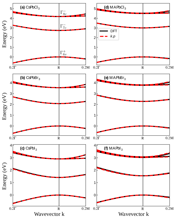
We calculated band structures for all considered materials using the presented model with the obtained parameter sets. As shown in Fig. 2, we get an excellent agreement between the DFT and the models in a considerable wide range of the BZ. In the case of MAPbX3, the 4-fold degenerated at the R point (for the exact cubic symmetry) block splits into two blocks of energies and . They are double degenerated due to spin (the Kramers‘ degeneracy). The splitting between them is given by . Since it is not very large (a few dozens of meV), the splitting is not visible in the figure.
V Material gain calculation
We calculate the material gain for bulk perovskites and compare the results to the values from reference materials: GaAs and InP. Details regarding the model for gain calculation are given in Refs. [42, 41, 40]. The gain was modeled according to the equation
where is a step in the -space, is the vacuum permitivity, m0 is the free electron mass and nr is refractive index. The summation indices and denote subbands within the conduction and valence band with the respective energies and . The energy diffeence at a given point is . The f(Ec;k, Fc) and f(Ev;k, Fv) are Fermi distribution functions for electrons and holes, respectively. They are calculated for given carrier density and give us quasi Fermi levels Fc and Fv. To model the allowed transitions, we take the Gaussian distribution function
with a full width at half maximum eV. For the calculations here, the Gaussian distribution was chosen, not Lorenz as in previous works [41, 40] due to the tail of the Lorentz distribution function. In the case of calculations made for perovskites, the Lorenz distribution caused additional noise in a forbidden area. The Gaussian distribution function is used for non-Markovian gain calculations [43, 44]. This kind of the line shape gain model gives good agreement with experimental gain spectra [45, 46]. One should note, that the band structure is fitted to the DFT simulations at K, while in the gain simulations we assume K.
VI Results and discussion
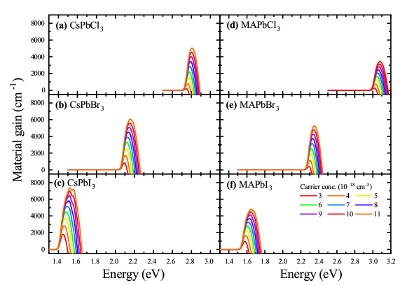
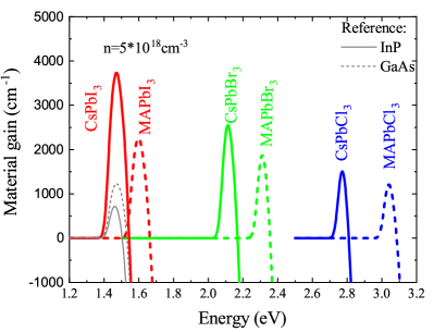
Figure 3 shows the results of material gain for CsPbCl3, CsPbBr3 and CsPbI3 (left panel); and for MAPbCl3, MAPbBr3 and MAPbI3 (right panel). They are calculated for carrier concentrations from to . It is clearly visible that for the given range of carrier concentrations, the positive material gain is observed for all considered materials. GaAs and InP were chosen as a reference. To compare the gain intensities for the investigated materials, we performed simulations for the concentration fixed to . The results are presented in Figure 4. The solid line shows calculations for CsPbX3 and the dashed line for perovskites with methyloamonium (MAPbX3). Red color corresponds to materials for which , for green , and for blue . The gray color shows the calculation for reference materials: the dashed line corresponds to GaAs and the solid line to InP. As clearly visible in the figure, for the same concentration, the gain calculated for perovskites has higher values than for the reference III-V materials.
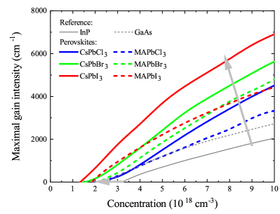
The maximum values of the gain as a function of carrier concentration are shown in Figure 5. Also, in this case, the difference between the gain calculated for perovskites and for the reference materials is pronounced. It can be seen that the highest gain values are obtained for X = I materials. As shown in Table LABEL:tab:params, CsPbI3 and MAPbI3 have the smallest effective masses for the valence band mv, i.e. 0.125 and 0.139, respectively. The medium values are obtained for X=Br materials, which corresponds to the masses for CsPbBr3 of 0.158 and 0.176 for MAPbBr3. The highest mv values of 0.189 and 0.210 appear for CsPbCl3 and MAPbCl3, which corresponds to the lowest gain value. A gray arrow has been drawn in the figure 5, pointing where the gain begins to be positive. We can see that for perovskites, we get a positive value for smaller concentrations of carriers than for GaAs and InP. This value can be directly converted into the density of the threshold current. Therefore, the gain for perovskites can be expected to be positive for lower current densities, as compared to the reference materials. These differences result directly from the band structure. An important difference between the perovskites and GaAs and InP is related to the symmetry of bands taking part in the fundamental transition. For the latter, the band gap is between the s-type conduction band and the heavy-hole/light-hole subbands. In contrast, for the considered perovskites the dominant transition is between the s-type valence band and the spin-orbit split-off subband of the conduction band. Higher gain values for perovskites are also related to a lower refractive index value compared to the reference materials.
VII Conclusions
In this work, we calculated the material gain for selected bulk perovskites: CsPbCl3, CsPbBr3, CsPbI3, MAPbCl3, MAPbBr3 and MAPbI3 within the eight-band model. We derived an invariant expansion form of the C4v Hamiltonian for perovskites. The material parameters of the model needed for the calculations were determined from the adjustment to the DFT calculations. It has been shown that the material gain for perovskites is stronger than for the reference GaAs and InP materials. Calculations indicate also that positive gain can be obtained at lower current densities than for the reference III-V compounds.
Acknowledgements.
We are grateful to Herbert Mączko for sharing his code for material gain simulations and to Paweł Scharoch for discussions.Appendix A Explicit form of the Hamiltonian in the JM basis
In this appendix, we present an explicit form of the Hamiltonian. The matrix is given in a basis of total angular momentum , , , , , , , . We took the basis definition following Ref. [36], which result in consistent form of invariant matrices, despite the fact that valence and conduction bands are inverted. The basis states in product form are given by
where , , , labels refers to the transformational properties under symmetry operations. According to the common convention, the states which are odd under the inversion operation are taken as purely imaginary, and the even ones are real [36].
| (4) |
where
References
- [1] L. Protesescu, S. Yakunin, M. I. Bodnarchuk, F. Krieg, R. Caputo, C. H. Hendon, R. X. Yang, A. Walsh, and M. V. Kovalenko, Nano Letters 15, 3692 (2015).
- [2] G. Nedelcu, L. Protesescu, S. Yakunin, M. I. Bodnarchuk, M. J. Grotevent, and M. V. Kovalenko, Nano Letters 15, 5635 (2015).
- [3] A. Dey, P. Rathod, and D. Kabra, Advanced Optical Materials 6, 1 (2018).
- [4] L. Lei, Q. Dong, K. Gundogdu, and F. So, Advanced Functional Materials 31, 1 (2021).
- [5] C. M. Mauck and W. A. Tisdale, Trends in Chemistry 1, 380 (2019).
- [6] F. Thouin, S. Neutzner, D. Cortecchia, V. A. Dragomir, C. Soci, T. Salim, Y. M. Lam, R. Leonelli, A. Petrozza, A. R. S. Kandada, and C. Silva, Phys. Rev. Mater. 2, 034001 (2018).
- [7] S. Kahmann, H. Duim, H. H. Fang, M. Dyksik, S. Adjokatse, M. Rivera Medina, M. Pitaro, P. Plochocka, and M. A. Loi, Advanced Functional Materials 31, (2021).
- [8] J. Fu, M. Li, A. Solanki, Q. Xu, Y. Lekina, S. Ramesh, Z. X. Shen, and T. C. Sum, Advanced Materials 33, 1 (2021).
- [9] F. Deschler, M. Price, S. Pathak, L. E. Klintberg, D. D. Jarausch, R. Higler, S. Hüttner, T. Leijtens, S. D. Stranks, H. J. Snaith, M. Atatüre, R. T. Phillips, and R. H. Friend, Journal of Physical Chemistry Letters 5, 1421 (2014).
- [10] P. Geiregat, J. Maes, K. Chen, E. Drijvers, J. De Roo, J. M. Hodgkiss, and Z. Hens, ACS Nano 12, 10178 (2018).
- [11] X. Chen, H. Lu, Y. Yang, and M. C. Beard, Journal of Physical Chemistry Letters 9, 2595 (2018).
- [12] T. Das, G. Di Liberto, and G. Pacchioni, The Journal of Physical Chemistry C 126, 2184 (2022).
- [13] Z. G. Yu, Scientific Reports 6, 28576 (2016).
- [14] R. Ben Aich, S. Ben Radhia, K. Boujdaria, M. Chamarro, and C. Testelin, J. Phys. Chem. Lett. 11, 808 (2020).
- [15] W. J. Fan, AIP Advances 8, 095206 (2018).
- [16] D. Ompong, G. Inkoom, and J. Singh, J. Appl. Phys. 128, 235109 (2020).
- [17] S. Boyer-Richard, C. Katan, B. Traoré, R. Scholz, J.-M. Jancu, and J. Even, J. Phys. Chem. Lett. 7, 3833 (2016).
- [18] M. Nestoklon, Comput. Mater. Sci. 196, 110535 (2021).
- [19] L. C. L. Y. Voon and M. Willatzen, The kp method: electronic properties of semiconductors (Springer Science & Business Media, 2009).
- [20] J. Even, L. Pedesseau, C. Katan, M. Kepenekian, J.-S. Lauret, D. Sapori, and E. Deleporte, J. Phys. Chem. C 119, 10161 (2015).
- [21] J. M. Luttinger, Phys. Rev. 102, 1030 (1956).
- [22] H. R. Trebin, U. Rössler, and R. Ranvaud, Phys. Rev. B 20, 686 (1979).
- [23] T. Eissfeller, Ph.D. thesis, Technical University of Munich, 2012.
- [24] R. Kashikar, M. Gupta, and B. R. K. Nanda, Phys. Rev. B 101, 155102 (2020).
- [25] P. Hohenberg and W. Kohn, Physical Review 136, B864 (1964).
- [26] W. Kohn and L. J. Sham, Physical Review 140, A1133 (1965).
- [27] G. Kresse and J. Furthmüller, Computational Materials Science 6, 15 (1996).
- [28] G. Kresse and J. Furthmüller, Physical Review B 54, 11169 (1996).
- [29] G. Kresse and D. Joubert, Physical Review B 59, 1758 (1999).
- [30] S. X. Tao, X. Cao, and P. A. Bobbert, Scientific Reports 7, 14386 (2017).
- [31] K. Lee, E. D. Murray, L. Kong, B. I. Lundqvist, and D. C. Langreth, Phys. Rev. B 82, 081101 (2010).
- [32] H. J. Monkhorst and J. D. Pack, Physical Review B 13, 5188 (1976).
- [33] A. V. Krukau, O. A. Vydrov, A. F. Izmaylov, and G. E. Scuseria, The Journal of Chemical Physics 125, (2006).
- [34] J. Even, L. Pedesseau, J.-M. Jancu, and C. Katan, The Journal of Physical Chemistry Letters 4, 2999 (2013).
- [35] A. D. Wright, C. Verdi, R. L. Milot, G. E. Eperon, M. A. Pérez-Osorio, H. J. Snaith, F. Giustino, M. B. Johnston, and L. M. Herz, Nature Communications 7, 11755 (2016).
- [36] R. Winkler, Spin-Orbit Coupling Effects in Two-Dimensional Electron and Hole Systems (Springer, 2003).
- [37] M. S. Dresselhaus, G. Dresselhaus, and A. A. Jorio, Group theory : application to the physics of condensed matter (Springer-Verlag, 2010).
- [38] G. L. Bir and G. E. Pikus, Symmetry and strain-induced effects in semiconductors (Wiley, 1974).
- [39] G. F. Koster, J. O. Dimmock, R. G. Wheeler, and H. Statz, The Properties of the Thirty-Two Point Groups (Research Monograph), 1963.
- [40] K. Gawarecki, P. Scharoch, M. Wiśniewski, J. Ziembicki, H. S. Mączko, M. Gładysiewicz, and R. Kudrawiec, Phys. Rev. B 105, 045202 (2022).
- [41] P. Scharoch, N. Janik, M. Wisniewski, H. S. Maczko, M. Gładysiewicz, M. P. Polak, and R. Kudrawiec, Comput. Mater. Sci. 187, 110052 (2021).
- [42] C. Ell, H. Haug, and S. W. Koch, Opt. Lett. 14, 356 (1989).
- [43] D. Ahn, IEEE Journal on Selected Topics in Quantum Electronics 1, 301 (1995).
- [44] W. Ingan, G. Quantum, S.-h. Park, D. Ahn, and S.-l. Chuang, Quantum 43, 1175 (2007).
- [45] S. H. Park, S. L. Chuang, J. Minch, and D. Ahn, Semiconductor Science and Technology 15, 203 (2000).
- [46] M. Gladysiewicz, R. Kudrawiec, G. Muziol, H. Turski, and C. Skierbiszewski, Adv. Phys. Res. 1 (2023).