Tiny Sc allows the chains to rattle: Impact of Lu and Y doping on the charge density wave in ScV6Sn6
Abstract
The kagome metals display an intriguing variety of electronic and magnetic phases arising from the connectivity of atoms on a kagome lattice. A growing number of these materials with vanadium kagome nets host charge density waves (CDWs) at low temperatures including ScV6Sn6, CsV3Sb5, and V3Sb2. Curiously, only the Sc version of the V6Sn6 HfFe6Ge6-type materials hosts a CDW (Gd–Lu, Y, Sc). In this study we investigate the role of rare earth size in CDW formation in the V6Sn6 compounds. Magnetization measurements on our single crystals of (Sc,Lu)V6Sn6 and (Sc,Y)V6Sn6 establish that the CDW is suppressed by substitution of Sc by larger Lu or Y. Single crystal x-ray diffraction reveals that compressible Sn-Sn bonds accommodate the larger rare earth atoms within loosely packed -Sn-Sn chains without significantly expanding the lattice. We propose that Sc provides the extra room in these chains crucial to CDW formation in ScV6Sn6. Our rattling chain model explains why both physical pressure and substitution by larger rare earths hinder CDW formation despite opposite impacts on lattice size. We emphasize the cooperative effect of pressure and rare earth size by demonstrating that pressure further suppresses the CDW in a Lu-doped ScV6Sn6 crystal. Our model not only addresses why a CDW only forms in the V6Sn6 materials with tiny Sc, it also advances to our understanding of why unusual CDWs form in the kagome metals.
keywords:
Charge density wave, intermetallic, stannide, chemical pressure, phase transition, magnetic susceptibility, pressure, x-ray diffraction, ScV6Sn6, RV6Sn6, LuV6Sn6, YV6Sn6, rare earth, phononCDW
1 Introduction
A charge density wave (CDW) is an ordered phase of a metallic crystal that appears on cooling. It is characterized by both localization of some conduction electrons and an associated atomic displacement which reduce the translational symmetry of the lattice 1, 2. CDWs show excellent tune-ability with physical pressure, chemical composition, and disorder 3, 4, 5, 6, 7, 8, 9, 10, 11. In fact, tuning the CDW transition to zero temperature is a good approach to discover new superconductors 12, 13, 14, 15, 16, 17, 18, 19.
Kagome metals have recently attracted significant interest for their unusual electronic and magnetic properties arising from kagome sheets of transition metals 21, 22, 23, 24, 25, 26, 27, 28, 29, 30, 31, 32, 33, 34, 35, 36, 37. A growing number of these materials display a CDW at low temperature, especially when vanadium forms the kagome net. The V3Sb5 materials ( = K, Rb, Cs) host both superconductivity and curious CDW phases 38, 39, 40, 23, 24, 25, 26, 41, 42, 43, 44, 45, 46, 47, 48, 49, 50. V3Sb2 likely has a CDW transition as well 51.
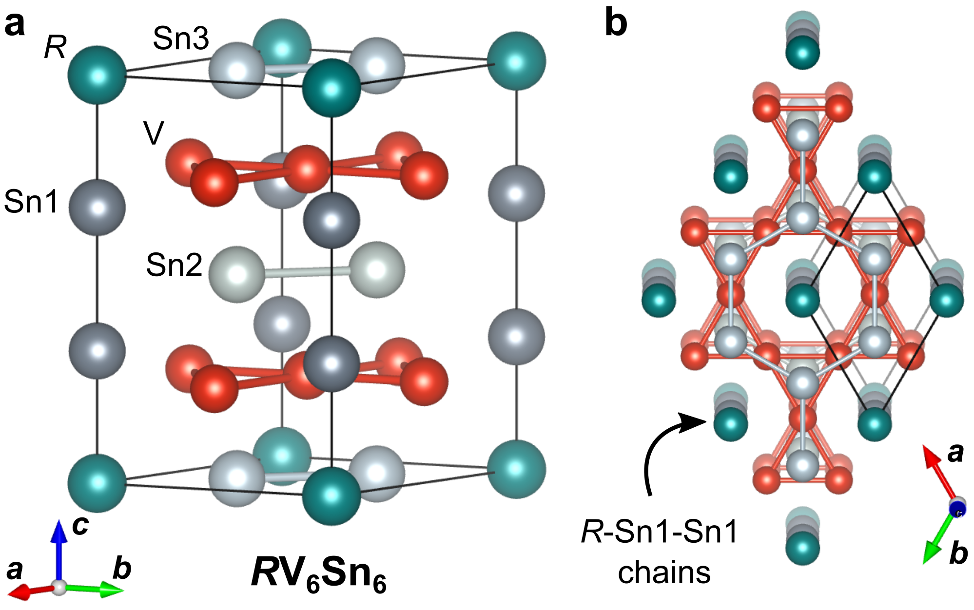
A CDW has also been identified in the vanadium-kagome metal ScV6Sn6 below 92 K 52. This is the Sc member of the rare earth V6Sn6 compounds ( = Sc, Y, and Gd–Lu)53, 54, 55. These adopt the hexagonal HfFe6Ge6 structure type (Fig. 1a) characterized by V-kagome sheets interleaved between Sn2-honeycomb and Sn3-honeycomb sheets. Rare earth atoms and Sn1 atoms form a chain that occupy channels in the hexagonal holes in the kagome and honeycomb layers as illustrated in Fig. 1b. These chains of atoms play a pivotal role in the CDW mode as they displace along the -axis in the modulated structure 52. Several CDW modes appear to compete in ScV6Sn6 56 demonstrated by the strong CDW fluctuations observed above the transition temperature57, 58 with impacts on the electrical transport properties 27.
It is important to note that the CDW in ScV6Sn6 has a wave vector 52, 57, 58 in contrast to that observed in the V3Sb5 materials ( or )40, 23, 25, 41, 42, 43, 59, 60. Another key difference is that the CDW in V3Sb5 compounds is dominated by vanadium displacements perpendicular to the hexagonal -axis 25. Numerous investigations of the electronic structure of ScV6Sn6 by photoemission measurements tie the CDW order to the Sn bands instead of the prominent vanadium bands 61, 62, 63, 64, 58, 65. There is evidence that the CDW phase has unusual characteristics including anomalous Hall-like responses 27, 66 and claims of time reversal symmetry breaking 67.
So far, none of the other V6Sn6 appear to host CDW order 55, 27, 68, 69, 70, 71, 54. What makes the scandium version special? One clue is that the CDW in ScV6Sn6 is suppressed by pressure and disappears before 2.4 GPa 72. Maybe lattice volume and rare earth size are important.
In this paper, we investigate the impact of rare earth size on CDW formation in the V6Sn6 materials by isovalent substitution of Lu and Y into ScV6Sn6. We synthesize single crystals of (Sc1-xLux)V6Sn6 and (Sc1-yYy)V6Sn6 and determine the CDW transition temperature with magnetization measurements. We find that the CDW phase is suppressed in both cases without significant impact on the lattice size. Detailed crystallography reveals that larger atoms are accommodated by extra room between the Sn1-Sn1 atoms along the -axis (Fig. 1a). We propose that this space in the loose -Sn1-Sn1 chains is crucial for CDW formation in ScV6Sn6. Our rattling chain model explains why the CDW is suppressed by pressure as well as by doping with larger rare earths despite their opposite impacts on lattice volume. We test our model by confirming that pressure reduces the CDW transition temperature in a sample where instability is already suppressed by Lu-doping. This study answers why only the Sc version of the V6Sn6 kagome metals hosts CDW order; the small Sc atoms provide extra room for -Sn1-Sn1 chains to rattle and permitting the CDW displacements. In addition this system exhibits an deviation from the usual correspondence between chemical and physical pressure.
2 Experimental
2.1 Crystal growth
Crystals of (Sc,Lu)V6Sn6 and (Sc,Y)V6Sn6 were grown from a Sn-rich melt following Arachchige et al. 52 Distilled scandium pieces (Alfa Aesar 99.9%), distilled Lutetium pieces (Alfa Aesar 99.9%), yttrium pieces (alfa aesar 99.9%), 3 mm pieces of vanadium slugs (Alfa Aesar 99.8%), and tin shot (Alfa Aesar 99.99+%) were added to 2 or 5 mL alumina Canfield crucible sets 73. An atomic ratio of Sc : Lu : V : Sn or Sc : Y : V : Sn = : : 6 : 60 was used for all growths. The crucibles were sealed in silica ampoules filled with about 0.2 atm argon. These were heated in a box furnace to 1150 °C over 12 h and held for 15 h to dissolve as much vanadium as possible. Crystals were grown during a 300 h slow cool to 780 °C. The ampoules were then removed from the furnace, inverted into a centrifuge and spun rapidly to fling the remaining liquid away from the crystals.
These growths yielded hard, light-gray metallic hexagonal crystals on crucible walls and vanadium pieces. Mirror-like basal, prismatic and pyramidal facets are common. The Sc and Lu rich crystals were 0.3–3 mm in size and tend to be blocky with some Sn inclusions. The most Y-rich crystals formed flatter hexagonal plates.
2.2 Characterization
Powder x-ray diffraction (XRD) was carried out using a Bruker D2 Phaser with Cu Kα source and Ni filter for phase identification and to determine lattice parameters.
Single crystal x-ray diffraction measurements at room temperature were carried out using a Rigaku XtaLAB PRO diffractometer. Data collection and integration were done using the Rigaku Oxford Diffraction CrysAlis Pro software 74 and the structural refinement was performed using a SHELXTL package 75, 76. Refined structures and .cif files of LuV6Sn6 and YV6Sn6 can be found in the supplemental materials.
Energy disperse spectroscopy (EDS) was performed to estimate the ratios of the rare earth elements. Crystals were mounted in Crystalbond and polished flat. EDS was carried out in a Zeiss EVO scanning electron microscope at 20 keV.
Magnetization measurements were carried out using a Quantum Design Magnetic Property Measurement System 3 using the Vibrating Sample Magnetometer (VSM) option. Crystals were etched in an aqueous 10 wt% HCl solution for 12-36 h to remove surface Sn then attached to a fused silica paddle with GE varnish. All measurements presented were measured with the field perpendicular to the hexagonal axis. The fraction of superconducting Sn in each sample was estimated by a 10 Oe zero field cooled measurement through the transition. Estimated beta-Sn fractions ranged from 0.5–7 vol%.
To check for superconductivity, resistance measurements down to 0.12 K were performed using the Adiabatic Demagnetization Refrigerator option in a Quantum Design Physical Property Measurement system using silver paste and platinum wire contacts. These results are presented in the supplemental materials.
Two single crystals of (Sc1-xLux)V6Sn6 and one LuV6Sn6 crystal were measured concurrently in the same piston cylinder pressure cell. Contacts were made between platinum wire and the samples using Epotek H20E silver epoxy, which was cured at 135°C for 30 minutes. Daphne 7575 was used as a pressure medium77 and the value of the pressure was calibrated using the fluorescence of a small ruby chip located near the crystals78. The pressure was recorded at room temperature and again at low temperature, by comparing with the values of fluorescence peaks from a ruby sample at ambient pressure. Resistance measurements were made for each sample using a Lakeshore 372 resistance bridge with 3708 preamp/scanner. The pressure cell was loaded into a Quantum Design Physical Property Measurement System (PPMS) where the temperature was controlled by cooling and warming at a rate of 0.5 K min-1 with about 50 Torr of helium exchange gas in the sample chamber. A calibrated Cernox thermometer was fixed to the outside of the pressure cell next to the copper sample wires to accurately determine the temperature of the measured crystals.
3 Results
3.1 Lattice trends
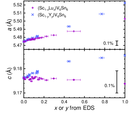
Figure 2 presents the evolution the lattice parameters as Y and Lu are doped into ScV6Sn6. and vary continuously across both series indicating that a complete solid solution exists. increases linearly across with a 0.52% and 0.88% expansion to LuV6Sn6 and YV6Sn6, respectively. The parameter increases weakly with Y doping (0.10%) and subtly decreases for the Lu series (-0.02%). Ionic radii provide an imperfect proxy of the size atoms in V6Sn6. The radii of Sc+3, Lu+3, and Y+3 are quoted as 0.87, 0.977, and 1.019 Å at 8-coordinated sites in oxide materials 79. Considering the Lu and Y ions are 12% and 17% larger than Sc, it is surprising that the changes in the lattice parameter are so weak across the substitution series.
3.2 Magnetization
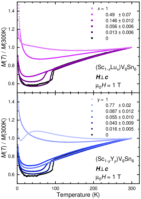
Next we will explore how Lu and Y substitution impacts the CDW in ScV6Sn6. Figure 3 presents the normalized magnetization curves for selected Lu and Y doped samples. The magnitude of the susceptibility at room temperature is comparable for all samples measured, ranging from 7.5–9.0 emu g-1 Oe-1 (6.2–8.2 cm3 (mol atom)-1) consistent with Pauli paramagnetism 80. The CDW transition in ScV6Sn6 manifests as a sharp drop of susceptibility on cooling through the first order transition52. This signature begins at 94 K (black) and shifts to lower temperatures with increasing Lu or Y content. At the same time, the size of drop decreases. The broadening of the transition step is likely due to chemical inhomogeneity observed by EDS.
3.3 Phase Diagrams
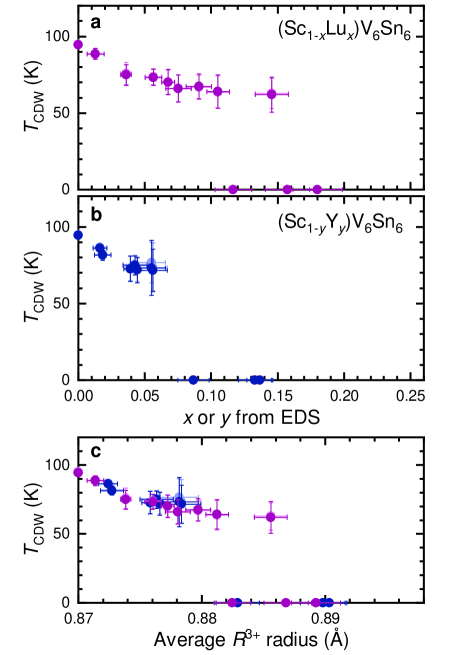
Figure 4a and b summarizes suppression of the CDW phase with Lu and Y substitution extracted from magnetization. falls smoothly then discontinuously around a critical doping ( and ) where we lose the step-like signature. This is not the usual behavior we expect for a quantum critical point were the transition temperature is smoothly reduced to 0 K.81 Instead, our CDW transition is first order so the phase can disappear more abruptly. No new transitions are observed at higher values of and .
It is important to note that less Y is required to destroy the CDW than Lu. This might arise from yttrium’s larger size. Figure 4c shows that the trend of vs average ionic radius has similar behavior for the Lu an Y series. The Lu and Y are also heavier atoms than Sc (174.97, 88.906, and 44.956 g mol-1, respectively). This could be playing a role in suppressing the CDW as proposed by Hu et al. 65. We suggest that this is less important than size because Lu is heavier than Y and we observe that less Y is needed to destabilize the CDW.
Suppression of a CDW can lead to superconductivity. ADR resistivity measurements revealed no evidence of superconductivity down to at least 150 mK in Lu doped samples with and as well as Y doped samples with and .
4 Discussion
To simplify our understanding of the evolution of phase transitions we often consider that chemical and mechanical pressure have the same impact on the electronic and lattice subsystems. If lattice volume has a strong impact on the stability of a phase, then we might expect the transition temperature to rise as we expand the lattice with doping (negative chemical pressure) and fall as we compress the lattice mechanically or through doping.
This correspondence between chemical and physical pressure is epitomized by the CDW and superconducting 3-4-13 Remeika phases. Specifically, the (Sr,Ca)3Ir4Sn13 and (Sr,Ca)3Rh4Sn13 substitution series (chemical pressure) exhibit common evolution of the CDW and superconducting critical temperatures with physical pressure11, 10.
Our investigation of the CDW evolution in isovalent doped ScV6Sn6 reveals behavior that deviates from the universal chemical-physical pressure picture. We observe that the decrease with negative chemical pressure as we substitute in the larger Lu and Y atom (Fig. 4). Zhang et al. reveal that physical pressure also reduces 72. The observation that CDW in ScV6Sn6 is suppressed in both cases suggests a new model is needed to explain this behavior.
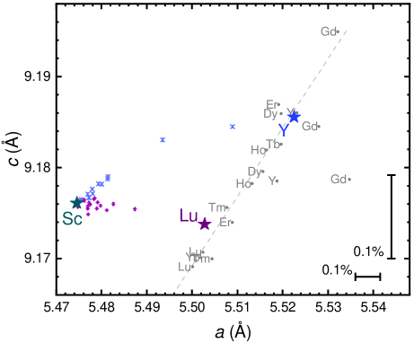
Let’s begin by looking at how the rare earth atom size actually impacts the lattice. Figure 5 illustrates how the and lattice parameters of V6Sn6 compounds depends on at room temperature. First, observe that most of the the lattice parameters of V6Sn6 compounds (gray points) lie on a linear trend (dashed line) with the smaller, late rare earths with smaller and . Sc is the smallest rare earth atom. If only the size matters, we might expect the lattice parameters of ScV6Sn6 (dark green star) to lie on the lower left of this trend. This is not the case. It has a smaller but a comparable to the Lu compound (purple star). Obviously, the lattice size is not simply controlled by the size of the rare earth atom. Our doping series emphasize this anomalous lattice evolution in Fig. 5 (small blue and purple symbols) as the lattice parameters interpolate between the end members.
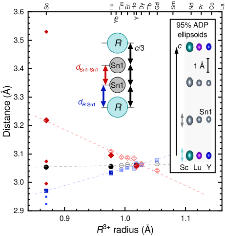
We have established that the lattice parameter has a nontrivial dependence on the rare earth ion. How are larger atoms accommodated in the crystal structure if is only weakly affected? Figure 6 presents the evolution of key bond distances with ionic radius across the V6Sn6 materials determined by single crystal XRD. To begin, note that larger rare earth atoms produce a larger -Sn1 bond distance (blue) but the lattice parameter (black, plotted as ) increases far more slowly. This requires that the Sn1-Sn1 distance must decrease (red). In other words, larger rare earths compress the Sn1-Sn1 bond with little impact on the unit cell height. Apparently, there is extra room in the -Sn1-Sn1 chain to accommodate larger atoms.
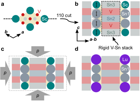
What is setting the size of if the -Sn1-Sn1 chain does not? We propose that the stack of V-kagome and Sn2/Sn3-honeycomb sheets do. Start by considering the V6Sn6 as two subsystems; -Sn1-Sn1 chains filling tubes in a superstructure of stacked V-kagome and Sn-honeycomb sheets (illustrated in Fig. 1b). Figure 7 depicts a cut along the (110) plane presenting the sections of V and Sn sheets as colored rectangles.
ScV6Sn6 and LuV6Sn6 have nearly identical values suggesting that the stacked Sn and V sheets are setting and small Sc atom leave the channels under-filled (Fig. 7b). This facilitates low-energy rattling displacements of the Sn1. This rattling is evident in the atomic displacement parameters (ADPs) from our single crystal XRD refinements (see supplemental materials). The -axis displacement parameters, , for the and Sn1 atoms are twice as large in ScV6Sn6 than in the Lu or Y compounds. We illustrate this difference in the inset of Fig. 6 by depicting the 95% displacement ellipsoids for the and Sn1 atoms. The Sc and Sn1 atoms in the first column show taller ellipsoids representing larger position deviations in this direction. This reflects the strong CDW fluctuation observed in ScV6Sn6 by inelastic and diffuse x-ray scattering 57, 58.
These are precisely the displacements that are most prominent in ScV6Sn6’s CDW phase. The small symbols in Fig. 6 are the bond lengths in the refined CDW structure of ScV6Sn6 from Arachchige et al. 52. The Sc-Sn1 bonds shrink a little (small blue dots) but, the Sn1-Sn1 bonds vary more dramatically (small red dots). Two Sn1-Sn1 distances shorten by 4.5% and 6.9% while the final third of bonds grow by 9.7%. These Sn1-Sn1 bonds are key feature of CDW and modify the Sn1 orbital states 58, 65.
We propose that the CDW instability needs the extra space in -Sn1-Sn1 for the modulations of Sn1-Sn1 distances observed in the CDW. If the column is packed too tightly by larger atoms or physical pressure, the displacements are penalized.
Next, we will examine how we might expect modifications of ScV6Sn6 to impact loose chains of -Sn1-Sn atoms and, the CDW this facilitates. Applying pressure suppresses to 0 K by 2.4 GPa 72. Pressure compresses the stack of V and Sn sheets (Fig. 7c). This constrains the chain of atoms which shortens the Sn1-Sn1 bonds. The CDW is penalized as the extra room in the chain is removed.
Doping ScV6Sn6 with Lu and Y quickly kills the CDW. In this case, introducing larger atoms fills up the extra room in the -Sn1-Sn1 chains (Fig. 7d), compressing the Sn1-Sn1 bonds and suppressing the CDW instability. This explains not only why Lu and Y doping suppress the CDW but also why no CDW transition is observed in V6Sn6 with bigger than Sc.
This rattling chain mechanism is distinct from the familiar correspondence between chemical and physical pressure. The CDW in ScV6Sn6 is suppressed by both lattice compression (physical pressure) and expansion by Lu/Y doping. Our model predicts that pressure and doping by larger rare earth should cooperate to reduce .
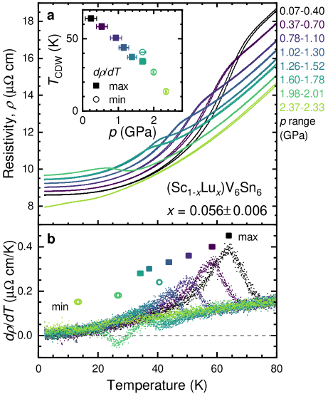
We test this prediction by monitoring the evolution of transition temperature with pressure in a crystal where the CDW is already partly suppressed by Lu-doping. Figure 8 presents the resistance vs temperature of (Sc0.944Lu0.056)V6Sn6 at a series of pressures. Near atmospheric pressure (black) the CDW transition is observed as a hysteretic drop in resistance on cooling at roughly 64 K. This drop-like feature decreases in temperature as pressure is increased until it changes character to a jump up on cooling for the highest two pressures (observed in pure ScV6Sn6 under pressure too 72). Applying pressure compresses the V-Sn stack around the already compacted -Sn1-Sn1 chain in the Lu-doped sample further penalizing the CDW displacements. This observation discredits the possibility that ScV6Sn6 has an optimal lattice volume for CDW formation. In that case applying pressure to the Lu-doped sample should re-stabilize the CDW and increase , but this is not what we observe (see supplemental materials).
5 Conclusions
In conclusion, we explored how rare earth size impacts CDW formation in the V6Sn6 family. Magnetization measurements on single crystals of (Sc,Lu)V6Sn6 and (Sc,Y)V6Sn6 revealed that the CDW transition temperature is reduced with increasing Lu and Y content. X-ray diffraction reveals enlightening lattice and bond-length trends. These observations and the evolution of the CDW under pressure motivate us to propose a rattling chain model for CDW formation in the V6Sn6 compounds. We assert that a CDW is only observed in the Sc version of the V6Sn6 compounds because the small Sc atom provide space for Sc and Sn1 atoms to rattle and permit the Sn1-Sn1 bond length modulation observed in the low temperature CDW phase. This model explains why both physical pressure and substitution of Sc by larger rare earth atoms suppresses CDW order. This is a curious variation to the usual corresponding effects of chemical and physical pressure on phase stability. In addition to explaining why ScV6Sn6 is special, our observations and model provide an important leap forward in our understanding of CDWs in the intriguing kagome metals.
We thank Bryan C. Chakoumakos of Oak Ridge National Laboratory for his helpful discussions with the single crystal x-ray refinements. W.R.M., H.W.S.A., C.L.A., J.D., and D.M. acknowledge support from the Gordon and Betty Moore Foundation’s EPiQS Initiative, Grant GBMF9069. S.M. and R.P.M. acknowledge the support from AFOSR MURI (Novel Light-Matter Interactions in Topologically Non-Trivial Weyl Semimetal Structures and Systems), grant# FA9550-20-1-0322. M.M. and H.B.C. were supported by the U.S. Department of Energy (DOE), Office of Science, Office of Basic Energy Sciences, Early Career Research Program Award KC0402020, under Contract DE-AC05-00OR22725. M.A.M. acknowledges support for adiabatic demagnetization refrigerator resistance measurements from the US Department of Energy, Office of Science, Basic Energy Sciences, Materials Sciences and Engineering Division. A portion of this research used resources at the Spallation Neutron Source, a DOE Office of Science User Facility operated by the Oak Ridge National Laboratory. A portion of this work was performed at the National High Magnetic Field Laboratory, which is supported by National Science Foundation Cooperative Agreement No. DMR-2128556 and the State of Florida.
The following files are available free of charge.
-
•
Supplementary information file including refined structures of LuV6Sn6 and YV6Sn6 as well resistance under pressure measurements for LuV6Sn6 and (Sc1-xLux)V6Sn6 with . Adiabatic demagnetization resistance measurements of doped ScV6Sn6 and LuV6Sn6 crystals are included as well.
-
•
LuV6Sn6_20230509.cif room temperature single crystal refinement of LuV6Sn6
-
•
YV6Sn6_20230519.cif room temperature single crystal refinement of YV6Sn6
References
- Zhu et al. 2017 Zhu, X.; Guo, J.; Zhang, J.; Plummer, E. W. Misconceptions associated with the origin of charge density waves. Advances in Physics: X 2017, 2, 622–640
- Grüner 1994 Grüner, G. Density waves in solids; Perseus Publishing, Cambridge, Mass., 1994
- Morosan et al. 2006 Morosan, E.; Zandbergen, H. W.; Dennis, B. S.; Bos, J. W. G.; Onose, Y.; Klimczuk, T.; Ramirez, A. P.; Ong, N. P.; Cava, R. J. Superconductivity in CuxTiSe2. Nature Physics 2006, 2, 544–550
- Joe et al. 2014 Joe, Y. I.; Chen, X. M.; Ghaemi, P.; Finkelstein, K. D.; de la Peña, G. A.; Gan, Y.; Lee, J. C. T.; Yuan, S.; Geck, J.; MacDougall, G. J.; Chiang, T. C.; Cooper, S. L.; Fradkin, E.; Abbamonte, P. Emergence of charge density wave domain walls above the superconducting dome in 1T-TiSe2. Nature Physics 2014, 10, 421–425
- Boubeche et al. 2021 Boubeche, M.; Yu, J.; Chushan, L.; Huichao, W.; Zeng, L.; He, Y.; Wang, X.; Su, W.; Wang, M.; Yao, D.-X.; Wang, Z.; Luo, H. Superconductivity and charge density wave in iodine-doped CuIrCuIr2Te4. Chinese Physics Letters 2021, 38, 037401
- Kazama et al. 2016 Kazama, T.; Maeda, M.; Takase, K.; Takano, Y.; Watanabe, T. Electric and magnetic properties of transition-metal carbide Sc3C4. 2016, 257, 34–37
- Sangeetha et al. 2012 Sangeetha, N. S.; Thamizhavel, A.; Tomy, C. V.; Basu, S.; Awasthi, A. M.; Ramakrishnan, S.; Pal, D. Interplay of superconductivity and charge density wave ordering in pseudoternary alloy compounds: Lu2Ir3(Si1-xGex)5, Lu2(Ir1-xRhx)3Si5, and (Lu1-xScx)2Ir3Si5. Physical Review B 2012, 86, 024524
- Li et al. 2023 Li, Z. et al. Suppressed charge-density-wave, robust ferromagnetism and Lifshitz transition in Sm2Ru3Ge5 crystal under high pressure. Journal of Alloys and Compounds 2023, 937, 168337
- Veiga et al. 2020 Veiga, L. S. I.; Mardegan, J. R. L.; v. Zimmermann, M.; Maimone, D. T.; Carneiro, F. B.; Fontes, M. B.; Strempfer, J.; Granado, E.; Pagliuso, P. G.; Bittar, E. M. Possible quantum fluctuations in the vicinity of the quantum critical point of (Sr, Ca)3Ir4Sn13 revealed by high-energy x-ray diffraction. Physical Review B 2020, 101, 104511
- Goh et al. 2015 Goh, S.; Tompsett, D.; Saines, P.; Chang, H.; Matsumoto, T.; Imai, M.; Yoshimura, K.; Grosche, F. Ambient pressure structural quantum critical point in the phase diagram of (CaxSr1-x)3Rh4Sn13. Physical Review Letters 2015, 114, 097002
- Klintberg et al. 2012 Klintberg, L. E.; Goh, S. K.; Alireza, P. L.; Saines, P. J.; Tompsett, D. A.; Logg, P. W.; Yang, J.; Chen, B.; Yoshimura, K.; Grosche, F. M. Pressure- and composition-induced structural quantum phase transition in the cubic superconductor (Sr,Ca)3Ir4Sn13. Physical Review Letters 2012, 109, 237008
- Sipos et al. 2008 Sipos, B.; Kusmartseva, A. F.; Akrap, A.; Berger, H.; Forró, L.; Tutiš, E. From Mott state to superconductivity in 1T-TaS2. Nature Materials 2008, 7, 960–965
- Briggs et al. 1980 Briggs, A.; Monceau, P.; Nunez-Regueiro, M.; Peyrard, J.; Ribault, M.; Richard, J. Charge density wave formation, superconductivity and Fermi surface determination in NbSe3: A pressure study. Journal of Physics C: Solid State Physics 1980, 13, 2117–2130
- Zocco et al. 2015 Zocco, D. A.; Hamlin, J. J.; Grube, K.; Chu, J.-H.; Kuo, H.-H.; Fisher, I. R.; Maple, M. B. Pressure dependence of the charge-density-wave and superconducting states in GdTe3, TbTe3, DyTe3. Physical Review B 2015, 91, 205114
- Zeng et al. 2021 Zeng, L.; Yan, D.; He, Y.; Boubeche, M.; Huang, Y.; Wang, X.; Luo, H. Effect of Ti substitution on the superconductivity of CuIr2Te4 telluride chalcogenide. Journal of Alloys and Compounds 2021, 885, 160981
- Aulestia et al. 2021 Aulestia, E. I. P.; Liu, X.; Pang, Y. Y.; So, C. W.; Yu, W. C.; Goh, S. K.; Lai, K. T. Pressure-induced enhancement of the superconducting transition temperature in La2O2Bi3AgS6. Journal of Physics: Condensed Matter 2021, 34, 06LT01
- Eckberg et al. 2019 Eckberg, C.; Campbell, D. J.; Metz, T.; Collini, J.; Hodovanets, H.; Drye, T.; Zavalij, P.; Christensen, M. H.; Fernandes, R. M.; Lee, S.; Abbamonte, P.; Lynn, J. W.; Paglione, J. Sixfold enhancement of superconductivity in a tunable electronic nematic system. Nature Physics 2019, 16, 346–350
- Lee et al. 2019 Lee, S.; de la Peña, G.; Sun, S. X.-L.; Mitrano, M.; Fang, Y.; Jang, H.; Lee, J.-S.; Eckberg, C.; Campbell, D.; Collini, J.; Paglione, J.; de Groot, F.; Abbamonte, P. Unconventional charge density wave order in the pnictide superconductor Ba(Ni1-xCox)2As2. Physical Review Letters 2019, 122, 147601
- Kudo et al. 2012 Kudo, K.; Takasuga, M.; Okamoto, Y.; Hiroi, Z.; Nohara, M. Giant phonon softening and enhancement of superconductivity by phosphorus doping of BaNi2As2. Physical Review Letters 2012, 109, 097002
- Momma and Izumi 2011 Momma, K.; Izumi, F. VESTA3 for three-dimensional visualization of crystal, volumetric and morphology data. Journal of Applied Crystallography 2011, 44, 1272–1276
- Teng et al. 2023 Teng, X. et al. Magnetism and charge density wave order in kagome FeGe. Nature Physics 2023,
- Meier et al. 2020 Meier, W. R.; Du, M.-H.; Okamoto, S.; Mohanta, N.; May, A. F.; McGuire, M. A.; Bridges, C. A.; Samolyuk, G. D.; Sales, B. C. Flat bands in the CoSn-type compounds. Physical Review B 2020, 102, 075148
- Liang et al. 2021 Liang, Z.; Hou, X.; Zhang, F.; Ma, W.; Wu, P.; Zhang, Z.; Yu, F.; Ying, J.-J.; Jiang, K.; Shan, L.; Wang, Z.; Chen, X.-H. Three-dimensional charge density wave and surface-dependent vortex-core states in a kagome superconductor CsV3Sb5. Physical Review X 2021, 11, 031026
- Kang et al. 2022 Kang, M. et al. Twofold van Hove singularity and origin of charge order in topological kagome superconductor CsV3Sb5. Nature Physics 2022, 18, 301–308
- Ortiz et al. 2021 Ortiz, B. R.; Teicher, S. M. L.; Kautzsch, L.; Sarte, P. M.; Ratcliff, N.; Harter, J.; Ruff, J. P. C.; Seshadri, R.; Wilson, S. D. Fermi surface mapping and the nature of charge-density-wave order in the kagome superconductor CsV3Sb5. Physical Review X 2021, 11, 041030
- Hu et al. 2022 Hu, Y.; Wu, X.; Ortiz, B. R.; Ju, S.; Han, X.; Ma, J.; Plumb, N. C.; Radovic, M.; Thomale, R.; Wilson, S. D.; Schnyder, A. P.; Shi, M. Rich nature of van Hove singularities in kagome superconductor CsV3Sb5. Nature Communications 2022, 13
- Mozaffari et al. 2023 Mozaffari, S. et al. Universal sublinear resistivity in vanadium kagome materials hosting charge density waves. 2023,
- Colman et al. 2011 Colman, R. H.; Sinclair, A.; Wills, A. S. Magnetic and crystallographic studies of Mg-herbertsmithite, -Cu3Mg(OH)6Cl2 - a new = 1/2 kagome magnet and candidate spin liquid. Chemistry of Materials 2011, 23, 1811–1817
- Wang et al. 2022 Wang, Y.; McCandless, G. T.; Wang, X.; Thanabalasingam, K.; Wu, H.; Bouwmeester, D.; van der Zant, H. S. J.; Ali, M. N.; Chan, J. Y. Electronic properties and phase transition in the kagome metal Yb0.5Co3Ge3. Chemistry of Materials 2022, 34, 7337–7343
- Miiller et al. 2011 Miiller, W.; Christensen, M.; Khan, A.; Sharma, N.; Macquart, R. B.; Avdeev, M.; McIntyre, G. J.; Piltz, R. O.; Ling, C. D. YCa3(VO)3(BO3)4: A kagomé compound based on vanadium(III) with a highly frustrated ground state. Chemistry of Materials 2011, 23, 1315–1322
- Gui and Cava 2022 Gui, X.; Cava, R. J. LaIr3Ga2: A superconductor based on a kagome lattice of Ir. Chemistry of Materials 2022, 34, 2824–2832
- Allison et al. 2022 Allison, M. C.; Wurmehl, S.; Büchner, B.; Vella, J. L.; Söhnel, T.; Bräuninger, S. A.; Klauss, H.-H.; Avdeev, M.; Marlton, F. P.; Schmid, S.; Ling, C. D. FeMn3Ge2Sn7O16: A perfectly isotropic 2-D kagomé lattice that breaks magnetic symmetry with partial spin order. Chemistry of Materials 2022, 34, 1369–1375
- Sales et al. 2022 Sales, B. C. et al. Chemical control of magnetism in the kagome metal CoSn1-xInx: Magnetic order from nonmagnetic substitutions. Chemistry of Materials 2022, 34, 7069–7077
- Thakur et al. 2020 Thakur, G. S.; Vir, P.; Guin, S. N.; Shekhar, C.; Weihrich, R.; Sun, Y.; Kumar, N.; Felser, C. Intrinsic anomalous Hall effect in Ni-substituted magnetic weyl semimetal Co3Sn2S2. Chemistry of Materials 2020, 32, 1612–1617
- McGuire et al. 2021 McGuire, M. A.; Zhang, Q.; Miao, H.; Luo, W.; Yoon, M.; Liu, Y.; Yilmaz, T.; Vescovo, E. Antiferromagnetic order and linear magnetoresistance in Fe-substituted shandite Co3In2S2. Chemistry of Materials 2021, 33, 9741–9749
- Meschke et al. 2021 Meschke, V.; Gorai, P.; Stevanović, V.; Toberer, E. S. Search and structural featurization of magnetically frustrated kagome lattices. Chemistry of Materials 2021, 33, 4373–4381
- Jovanovic and Schoop 2022 Jovanovic, M.; Schoop, L. M. Simple chemical rules for predicting band structures of kagome materials. Journal of the American Chemical Society 2022, 144, 10978–10991
- Ortiz et al. 2019 Ortiz, B. R.; Gomes, L. C.; Morey, J. R.; Winiarski, M.; Bordelon, M.; Mangum, J. S.; Oswald, I. W. H.; Rodriguez-Rivera, J. A.; Neilson, J. R.; Wilson, S. D.; Ertekin, E.; McQueen, T. M.; Toberer, E. S. New kagome prototype materials: discovery of KV3Sb5, RbV3Sb5, and CsV3Sb5. Physical Review Materials 2019, 3, 094407
- Ortiz et al. 2021 Ortiz, B. R.; Sarte, P. M.; Kenney, E. M.; Graf, M. J.; Teicher, S. M. L.; Seshadri, R.; Wilson, S. D. Superconductivity in the Z2 kagome metal KV3Sb5. Physical Review Materials 2021, 5, 034801
- Ortiz et al. 2020 Ortiz, B. R.; Teicher, S. M. L.; Hu, Y.; Zuo, J. L.; Sarte, P. M.; Schueller, E. C.; Abeykoon, A. M. M.; Krogstad, M. J.; Rosenkranz, S.; Osborn, R.; Seshadri, R.; Balents, L.; He, J.; Wilson, S. D. CsV3Sb5: A Z2 topological kagome metal with a superconducting grounds state. Physical Review Letters 2020, 125, 247002
- Nie et al. 2022 Nie, L. et al. Charge-density-wave-driven electronic nematicity in a kagome superconductor. Nature 2022, 604, 59–64
- Wang et al. 2021 Wang, Z. et al. Electronic nature of chiral charge order in the kagome superconductor CsV3Sb5. Physical Review B 2021, 104, 075148
- Li et al. 2021 Li, H. et al. Observation of unconventional charge density wave without acoustic phonon anomaly in kagome superconductors V3Sb5 ( = Rb, Cs). Physical Review X 2021, 11, 031050
- Yu et al. 2021 Yu, F. H.; Wu, T.; Wang, Z. Y.; Lei, B.; Zhuo, W. Z.; Ying, J. J.; Chen, X. H. Concurrence of anomalous Hall effect and charge density wave in a superconducting topological kagome metal. Physical Review B 2021, 104, l041103
- Jiang et al. 2021 Jiang, Y.-X. et al. Unconventional chiral charge order in kagome superconductor KV3Sb5. Nature Materials 2021, 20, 1353–1357
- Yang et al. 2020 Yang, S.-Y.; Wang, Y.; Ortiz, B. R.; Liu, D.; Gayles, J.; Derunova, E.; Gonzalez-Hernandez, R.; Šmejkal, L.; Chen, Y.; Parkin, S. S. P.; Wilson, S. D.; Toberer, E. S.; McQueen, T.; Ali, M. N. Giant, unconventional anomalous Hall effect in the metallic frustrated magnet candidate, KV3Sb5. Science Advances 2020, 6
- Yu et al. 2021 Yu, F. H.; Ma, D. H.; Zhuo, W. Z.; Liu, S. Q.; Wen, X. K.; Lei, B.; Ying, J. J.; Chen, X. H. Unusual competition of superconductivity and charge-density-wave state in a compressed topological kagome metal. Nature Communications 2021, 12
- Du et al. 2021 Du, F.; Luo, S.; Ortiz, B. R.; Chen, Y.; Duan, W.; Zhang, D.; Lu, X.; Wilson, S. D.; Song, Y.; Yuan, H. Pressure-induced double superconducting domes and charge instability in the kagome metal KV3Sb5. Physical Review B 2021, 103, l220504
- Oey et al. 2022 Oey, Y. M.; Ortiz, B. R.; Kaboudvand, F.; Frassineti, J.; Garcia, E.; Cong, R.; Sanna, S.; Mitrović, V. F.; Seshadri, R.; Wilson, S. D. Fermi level tuning and double-dome superconductivity in the kagome metal CsV3Sb5-xSnx. Physical Review Materials 2022, 6, l041801
- Yin et al. 2021 Yin, Q.; Tu, Z.; Gong, C.; Fu, Y.; Yan, S.; Lei, H. Superconductivity and normal-state properties of kagome metal RbV3Sb5 single crystals. Chinese Physics Letters 2021, 38, 037403
- Wang et al. 2022 Wang, N. et al. A density-wave-like transition in the polycrystalline V3Sb2 sample with bilayer kagome lattice. Chinese Physics B 2022, 31, 017106
- Arachchige et al. 2022 Arachchige, H. W. S.; Meier, W. R.; Marshall, M.; Matsuoka, T.; Xue, R.; McGuire, M. A.; Hermann, R. P.; Cao, H.; Mandrus, D. Charge Density Wave in Kagome Lattice Intermetallic ScV6Sn6. Physical Review Letters 2022, 129, 216402
- Romaka et al. 2011 Romaka, L.; Stadnyk, Y.; Romaka, V.; Demchenko, P.; Stadnyshyn, M.; Konyk, M. Peculiarities of component interaction in (Gd, Er)-V-Sn ternary systems at 870 K and crystal structure of V6Sn6 stannides. Journal of Alloys and Compounds 2011, 509, 8862–8869
- Zhang et al. 2022 Zhang, X. X.; Liu, Z. Y.; Cui, Q.; Wang, N. N.; Shi, L. F.; Zhang, H.; Dong, X. L.; Sun, J. P.; Dun, Z. L.; Cheng, J. G. Electronic and magnetic properties of intermetallic kagome magnets V6Sn6 ( = Tb - Tm). 2022,
- Lee and Mun 2022 Lee, J.; Mun, E. Anisotropic magnetic property of single crystals V6Sn6 ( = Y, Gd - Tm, Lu). Physical Review Materials 2022, 6, 083401
- Tan and Yan 2023 Tan, H.; Yan, B. Abundant lattice instability in kagome metal ScV6Sn6. 2023,
- Cao et al. 2023 Cao, S.; Xu, C.; Fukui, H.; Manjo, T.; Shi, M.; Liu, Y.; Cao, C.; Song, Y. Competing charge-density wave instabilities in the kagome metal ScV6Sn6. 2023,
- Korshunov et al. 2023 Korshunov, A. et al. Softening of a flat phonon mode in the kagome ScV6Sn6. 2023,
- Neupert et al. 2022 Neupert, T.; Denner, M. M.; Yin, J.-X.; Thomale, R.; Hasan, M. Z. Charge order and superconductivity in kagome materials. Nature Physics 2022, 18, 137–143
- Mu et al. 2021 Mu, C.; Yin, Q.; Tu, Z.; Gong, C.; Lei, H.; Li, Z.; Luo, J. -wave superconductivity in kagome metal CsV3Sb5 revealed by 121/123Sb NQR and 51V NMR measurements. Chinese Physics Letters 2021, 38, 077402
- Cheng et al. 2023 Cheng, S. et al. Nanoscale visualization and spectral fingerprints of the charge order in ScV6Sn6 distinct from other kagome metals. 2023,
- Kang et al. 2023 Kang, S.-H.; Li, H.; Meier, W. R.; Villanova, J. W.; Hus, S.; Jeon, H.; Arachchige, H. W. S.; Lu, Q.; Gai, Z.; Denlinger, J.; Moore, R.; Yoon, M.; Mandrus, D. Emergence of a new band and the Lifshitz transition in kagome metal ScV6Sn6 with charge density wave. 2023,
- Hu et al. 2023 Hu, Y. et al. Phonon promoted charge density wave in topological kagome metal ScV6Sn6. 2023,
- Lee et al. 2023 Lee, S.; Won, C.; Kim, J.; Yoo, J.; Park, S.; Denlinger, J.; Jozwiak, C.; Bostwick, A.; Rotenberg, E.; Comin, R.; Kang, M.; Park, J.-H. Nature of charge density wave in kagome metal ScV6Sn6. 2023,
- Hu et al. 2023 Hu, H.; Jiang, Y.; Călugăru, D.; Feng, X.; Subires, D.; Vergniory, M. G.; Felser, C.; Blanco-Canosa, S.; Bernevig, B. A. Kagome materials I: SG 191, ScV6Sn6. Flat phonon soft modes and unconventional CDW formation: Microscopic and effective theory. 2023,
- Yi et al. 2023 Yi, C.; Feng, X.; Yanda, P.; Roychowdhury, S.; Felser, C.; Shekhar, C. Charge density wave induced anomalous Hall effect in kagome ScV6Sn6. 2023,
- Guguchia et al. 2023 Guguchia, Z. et al. Hidden magnetism uncovered in charge ordered bilayer kagome material ScV6Sn6. 2023,
- Pokharel et al. 2022 Pokharel, G.; Ortiz, B.; Chamorro, J.; Sarte, P.; Kautzsch, L.; Wu, G.; Ruff, J.; Wilson, S. D. Highly anisotropic magnetism in the vanadium-based kagome metal TbV6Sn6. Physical Review Materials 2022, 6, 104202
- Pokharel et al. 2021 Pokharel, G.; Teicher, S. M. L.; Ortiz, B. R.; Sarte, P. M.; Wu, G.; Peng, S.; He, J.; Seshadri, R.; Wilson, S. D. Electronic properties of the topological kagome metals YV6Sn6 and GdV6Sn6. Physical Review B 2021, 104, 235139
- Ishikawa et al. 2021 Ishikawa, H.; Yajima, T.; Kawamura, M.; Mitamura, H.; Kindo, K. GdV6Sn6: A multi-carrier metal with non-magnetic 3-electron kagome bands and 4-electron magnetism. Journal of the Physical Society of Japan 2021, 90
- Rosenberg et al. 2022 Rosenberg, E.; DeStefano, J. M.; Guo, Y.; Oh, J. S.; Hashimoto, M.; Lu, D.; Birgeneau, R. J.; Lee, Y.; Ke, L.; Yi, M.; Chu, J.-H. Uniaxial ferromagnetism in the kagome metal TbV6Sn6. Physical Review B 2022, 106, 115139
- Zhang et al. 2022 Zhang, X.; Hou, J.; Xia, W.; Xu, Z.; Yang, P.; Wang, A.; Liu, Z.; Shen, J.; Zhang, H.; Dong, X.; Uwatoko, Y.; Sun, J.; Wang, B.; Guo, Y.; Cheng, J. Destabilization of the charge density wave and the absence of superconductivity in ScV6Sn6 under high pressures up to 11 GPa. Materials 2022, 15, 7372
- Canfield et al. 2016 Canfield, P. C.; Kong, T.; Kaluarachchi, U. S.; Jo, N. H. Use of frit-disc crucibles for routine and exploratory solution growth of single crystalline samples. Philos. Mag. 2016, 96, 84–92
- 74 CrysAlisPRO. Oxford Diffraction/Agilent Technologies UK Ltd, Yarnton, England
- Sheldrick 2015 Sheldrick, G. M. Crystal structure refinement with SHELXL. Acta Crystallographica Section C Structural Chemistry 2015, 71, 3–8
- Sheldrick 2015 Sheldrick, G. M. SHELXT Integrated space-group and crystal-structure determination. Acta Crystallographica Section A Foundations and Advances 2015, 71, 3–8
- Staško et al. 2020 Staško, D.; Prchal, J.; Klicpera, M.; Aoki, S.; Murata, K. Pressure media for high pressure experiments, Daphne oil 7000 series. High Pressure Research 2020, 40, 525–536
- Piermarini et al. 1975 Piermarini, G. J.; Block, S.; Barnett, J. D.; Forman, R. A. Calibration of the pressure dependence of the ruby fluorescence line to 195 kbar. Journal of Applied Physics 1975, 46, 2774–2780
- Shannon 1976 Shannon, R. D. Revised effective ionic radii and systematic studies of interatomic distances in halides and chalcogenides. Acta Cryst. 1976, A32, 751–767
- Kittel 2004 Kittel, C. Introduction to solid state physics, eighth ed.; John Wiley & Sons Inc: Hoboken, NJ, 2004
- Coleman and Schofield 2005 Coleman, P.; Schofield, A. J. Quantum criticality. Nature 2005, 433, 226–229
- Guo et al. 2022 Guo, K.; Ye, J.; Guan, S.; Jia, S. Triangular Kondo lattice in YbV6Sn6 and its quantum critical behaviors in magnetic field. 2022,