Two-dimensional heavy fermion in a monoatomic-layer Kondo lattice YbCu2
The Kondo effect between localized -electrons and conductive carriers leads to exotic physical phenomena. Among them, heavy-fermion (HF) systems, in which massive effective carriers appear due to the Kondo effect, have fascinated many researchers. Dimensionality is also an important characteristic of the HF system, especially because it is strongly related to quantum criticality [S. Sachdev, Science 288, 475 (2000)]. However, perfect two-dimensional (2D) HF materials have not been reported yet. Here, we report the surface electronic structure of the monoatomic-layer Kondo lattice YbCu2 on a Cu(111) surface observed by synchrotron-based angle-resolved photoelectron spectroscopy. The 2D conducting band and the Yb 4 state, located very close to the Fermi level, are observed. These bands are hybridized at low-temperature, forming the 2D HF state, with an evaluated coherent temperature of about 30 K. The effective mass of the 2D state is enhanced by a factor of 100 by the development of the HF state. Furthermore, clear evidence of the hybridization gap formation in the temperature dependence of the Kondo-resonance peak has been observed below the coherent temperature. Our study provides a new candidate as an ideal 2D HF material for understanding the Kondo effect at low dimensions.
Heavy fermion (HF) systems in rare-earth (RE) intermetallic compounds originating from hybridization between localized -electrons and conduction electrons, namely - hybridization, are central topics in the field of the strongly-correlated electron systems [1]. At low temperatures, depending on the strength of the - hybridization, the physical properties change from itinerant electrons because of the Kondo effect or magnetic order originating from the magnetic moment of localized electrons due to Ruderman-Kittel-Kasuya-Yosida (RKKY) interactions. The competition between itinerant and localized characters of the -electrons make a quantum critical point (QCP), resulting in the emergence of fertile quantum phenomena such as non-Fermi liquid behavior, and non-BCS HF superconductivity [2, 3].
On the other hand, the dimensionality in the system characterizes the fundamental physical property. In low-dimensional systems, the enhancement of the electron-electron correlation and/or breaking of the inversion symmetry leads to novel quantum states such as Rashba-type spin-splitting [4], Tomonaga–Luttinger liquid [5, 6], and unconventional superconductivity [7, 8]. The combination of the HF state and low dimensionality modifies the ground state of the system because the order parameter of these systems is much more sensitive to dimensionality [9]. The ground state of two-dimensional (2D) HF can be easily controlled to the vicinity of a quantum critical point, which is the host to realize unconventional physical properties such as HF superconductivity, by simple external fields such as gate-tuning [10, 11], and surface doping [12] in addition to traditional external perturbations; temperature, pressure, and magnetic field. The fabrication of artificial low-dimensional strongly-correlated electron systems is one of the suitable methods to investigate the novel electronic phase. In the Ce-based artificial superlattice, the suppression of antiferromagnetic (AFM) ordering as well as the increase of the effective electron mass with decreasing of the thickness of the Ce-layer [13] and the emergence of the strong-coupling superconductivity [14] have been reported. To understand the fundamental properties of 2D HF systems, it is necessary to clarify the electronic band structure and the formation mechanism of the HF. However, the details have remained unclear due to the lack of promising materials and the extremely low transition temperatures of less than a few K to HF even in known materials [13, 15, 16].
The growth of the well-ordered atomically thin film on a single crystal substrate is a suitable technique to access such 2D electron systems. So far, various 2D Kondo-lattice has been fabricated on the substrates; multilayer CePt5 thin-film on Pt(111) [17], CePb3 on Si(111) [18], Graphene on SmB6 [19], and a checkerboard pattern of organic molecules on Au(111) [20]. However, Yb-based 2D HF material, in which the Yb ion is the most fundamental element to realize HF [21, 22] and has a symmetrical electronic-hole configuration to the Ce one, has not been reported. In particular, the RE-based monoatomic layer Kondo-lattice showing HF state has never been reported.
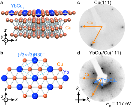
In this study, we report the HF electronic structure of a novel Yb-based monoatomic layer Kondo lattice; synchrotron-based angle-resolved photoelectron spectroscopy (ARPES) on monoatomic layered YbCu2 on Cu(111). The surface atomic structure of the YbCu2 on Cu(111) is shown in Fig. 1(a). The Yb atoms surrounded by Cu atoms are arrayed in a triangular lattice. In a similar surface alloy RE NM2/NM(111) (NM = noble metal), various physical properties appear such as FM ordering [23, 24, 25] and Weyl nodal-line fermion [26] depending on the containing RE element, but there is no report on the appearance of HF character so far. Figures 1(c) and 1(d) show the LEED patterns of the Cu(111) substrate and the Yb-adsorbed Cu(111) surface at 70 K, respectively. In addition to the primitive (1) spots originating from Cu(111) substrate indicated by yellow allows, the ()R30∘ structure with the Moiré patterns, originating from the small lattice mismatch between Cu(111) and the topmost surface alloy layer, was observed, indicating the successful fabrication of the monoatomic YbCu2 layer, one possible model of the Yb-Cu surface alloy system, on the Cu(111) substrate. Note that the overall trend of the LEED patterns is consistent with those of other RE NM2/NM(111) systems [27, 28, 29, 25, 23, 24].
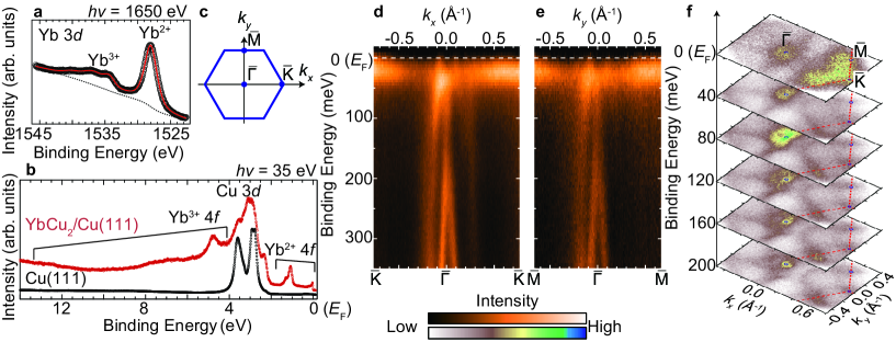
The itinerant or localized character of Yb 4 electrons is strongly reflected in the valency of the Yb ions. Figure 2(a) shows Yb 3 core-level spectrum of YbCu2/Cu(111) at 15 K. The photoelectron peaks at the binding energies of 1528 and 1538 eV originate from the Yb2+ and Yb3+ final states, respectively, after photoexcitation. From the intensity ratio between the Yb2+ and Yb3+ peaks after subtracting the background indicated by the dotted line in the figure, the mean valence of Yb ions was evaluated as 2.41 0.01. To confirm the consistency of the coexistence of Yb2+ and Yb3+ observed in the Yb 3 core-level spectra to the electronic state near the Fermi level (), angle-integrated valence-band photoelectron spectra of the Cu(111) clean substrate and the YbCu2/Cu(111) surface are shown in Fig. 2(b). The Cu 3 states at the binding energy of 3 eV are dominant in the Cu(111) substrate. In the YbCu2/Cu(111) spectrum, there are two narrow peaks originating from the Yb spin-orbit pair near and broad peaks of Yb final states and Cu 3 states at the binding energy of 3–13 eV. These results strongly suggest that the Yb ions in monoatomic layer YbCu2 are mixed valence. Note that in the YbAu2/Au(111), which has a similar atomic structure to YbCu2/Cu(111), Yb ions are almost divalent [28]. The reason for the difference in the Yb valence between YbCu2 and YbAu2 would be due to the in-plane lattice compression, which can be explained by the analogy from the bulk Yb-based intermetallic compounds under high pressure [30], because the lattice constant of bulk Cu is about 10 % smaller than that of Au. The lattice compression would promote the valence transition from Yb2+ to Yb3+ due to the smaller ionic radius of Yb3+ than that of Yb2+, realizing a mixed-valence state in YbCu2/Cu(111).
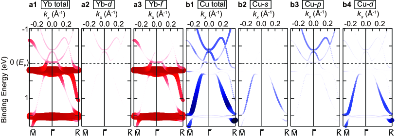
Figures 2(d,e) show ARPES band dispersions at 10 K along – and –, respectively, in the hexagonal surface Brillouin zone (SBZ) shown in Fig. 2(c). The flat band is close to and highly dispersive bands are observed near the point. According to the previous study and the DFT calculation for other RE NM2/NM(111) families, the flat band and well-dispersive bands mainly originate from the Yb2+ 4 and the mixing of the Yb 5 and Cu and orbitals, respectively [24, 28, 31]. The detailed assignments of these bands are shown in Supplementary Note 1. It should be noted that the photoelectron intensities of the dispersive band near the point at the positive wavenumber region are relatively weak in both – and – directions due to a photoexcitation selection rule [32]. The energy position of the Yb2+ 4 is very close to , which is the general feature of the Yb-based HF system such as -YbAlB4 [21] and YbRh2Si2 [22], suggesting the same mixed valent character of Yb ions in YbCu2/Cu(111) as the result of Yb 3 peaks. It should be noted that the surface electronic structure of almost all HF materials tends to be localized, which is inconsistent with that of the bulk, due to a surface lattice expansion. It should also be noted that the Yb-ions in bulk YbCu2 are mixed-valent [33, 34], which is similar to YbCu2/Cu(111), but the orthorhombic crystal structure is different from that of YbCu2/Cu(111). Additionally, the surface state of bulk YbCu2 is divalent, which is consistent with other Yb compounds. Therefore, the origin of the mixed-valent character of YbCu2/Cu(111) is not the same as that of bulk YbCu2.
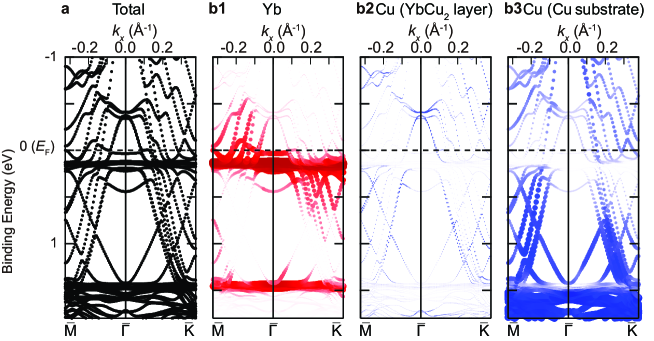
In Figures 2(d,e), the Yb2+ 4 flat band is modulated at the cross points to the conduction bands just below , which is evidence of - hybridization [35]. It should be noted that the - hybridization bands can appear in periodically located Yb and Cu atoms on the surface, not in randomly diluted Yb impurities in bulk Cu. The hole bands at the point and the Yb2+ 4 states near can be confirmed to originate from the YbCu2 layer by calculations [24, 28, 31] (see Supplimentary Fig.S2). Figure 2(f) shows a series of the constant energy contours of the YbCu2/Cu(111) surface. In the map at the binding energy of 0 eV, which corresponds to the experimental Fermi surfaces, there are strong photoelectron intensity areas at point and near the zone boundary. However, as shown in Figs. 2(d,e), non-bonding 4 character only appears near the and points, but the - hybridization feature only exhibits near the point. Therefore, in the following part, we focus on the hybridized band around the point to investigate the detail of the HF character appearing in monoatomically layered YbCu2.
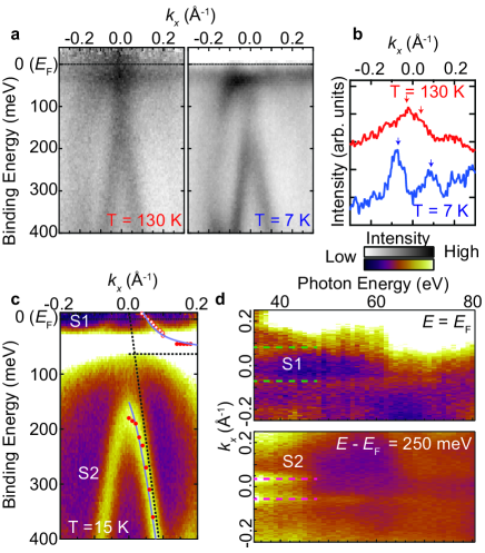
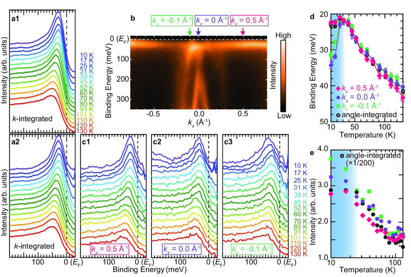
In the HF system, the size of the Fermi surface is modulated by the changing of the temperature due to the enhancement of the - hybridization. Figure 3(a) shows the temperature-dependent ARPES images along –. The overall trend of those images is consistent except near . To reveal the change of the dispersion at in more detail, the momentum-distribution curves (MDCs) at are plotted in Fig. 3(b). The peak position of the hybridized band near the point at 130 K is shifted toward a higher wavenumber at 7 K, suggesting an enlargement of the Fermi surface by the development of the - hybridization at low temperature.
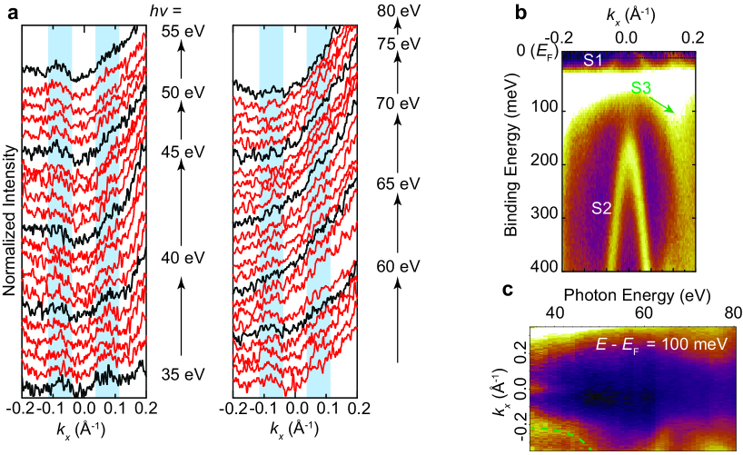
Figure 3(c) shows the ARPES image around the point taken with circularly polarized photons at 15 K. The - hybridization branches S1 and S2 are visible. To determine the dimensionality of the - hybridization bands, the photon-energy dependence of ARPES was measured as shown in Fig. 3(d). Both S1 and S2 bands show no photon-energy dependence, indicating no out-of-plane () dispersion. These experimental results strongly suggest that the - hybridization band is formed in the 2D YbCu2 plane. To evaluate the - hybridization feature, comparing it to the periodic Anderson model (PAM) is useful [36]. In the case of the electron correlation is zero or infinity, the band dispersions of PAM is explained as
| (1) |
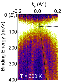
where and are the dispersions of the conduction band and the 4 band, respectively, and is the hybridization intensity. For the fitting by the PAM, a -linear hole band dispersion was assumed for the conduction band to reproduce the steep band shape observed by ARPES. The fitting results are shown in Fig. 2(c). The filled and break lines indicate the band dispersions with = 120 meV and 0 meV, respectively. The detailed process of fitting by the PAM is shown in Supplementary Note 5. By comparing the experimentally obtained heavy conduction band at 15 K and the simulated bare conduction band, a mass enhancement factor between the effective mass of the HF state at 15 K and unhybridized one () is evaluated as about 120 suggesting the appearance of heavy quasiparticles at low temperatures.
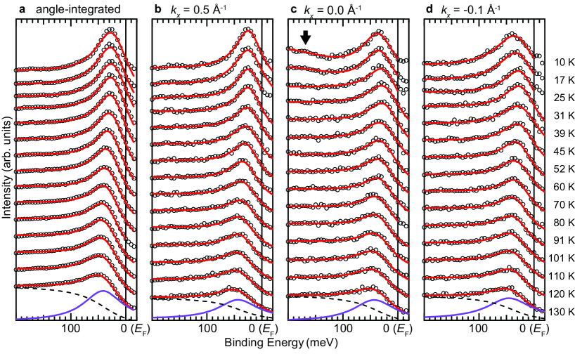
We now discuss the temperature dependence of the quasiparticle peak just below , so-called Kondo resonance (KR) peak. In the HF system, the temperature dependences of the energy position and intensity of the KR peak are reflected in the spectral weight transfer between 4 state and the conduction band as well as renormalization due to the development of the - hybridization. Figure 4(a1) shows the angle-integrated photoelectron intensity near as a function of temperature, and Fig. 4(a2) is the same, but the intensities are divided by the Fermi-Dirac distribution function convolved with the instrumental resolution. The KR peak energy is shifted to the side with decreasing temperature, indicating the evolution of the renormalization due to the HF formation. To discuss the temperature-dependent development of the HF state in more detail, the peak positions and intensities are obtained from the fitting of Fig. 4(a2) by a Lorentz function after subtracting a Shirley-type background, as shown in Figs. 4(d,e). The peak position shifts from 42 meV to 22 meV with decreasing temperature and is saturated at 30 K. The integrated intensity increases with decreasing temperature and is also saturated at 30 K. According to photoelectron spectroscopic studies of bulk RE intermetallic compounds, such saturated temperature represents a coherent temperature (), at which the - hybridization state is fully established, resulting in a HF state [37, 38]. The above experimental fact strongly suggests that YbCu2 is the 2D monoatomic-layered HF material with = 30 K, which is more valence fluctuative than other low-dimensional HF such as CeIn3/LaIn3 superlattice ( = 1.6 K) [13].
To investigate the momentum-dependent - hybridization formation, we took the temperature-dependent peak position and intensity of the quasiparticle peak at three wavenumbers ( = 0.5, 0.0, Å-1) as shown in Figs. 4(d, e). The change of the peak position at = 0.5 Å-1, which is the cut only the Yb2+ 4 state, almost follows the angle-integrated one. This suggests that the angle-integrated spectrum mainly focuses on the high-density Yb2+ 4 state and the renormalization is effective for all 4 states. In contrast to the saturated feature in the angle-integrated spectrum at = 30 K, the KR peak positions at = 0.0 and Å-1 are shifted toward the higher-binding energy side below of YbCu2 suggesting the hybridization gap enlargement, even though the peak shifts at = 0.0 and Å-1 also follows the angle-integrated peak above . Also, the peak intensity, which corresponds to the spectral weight transfer between Yb 4 states and conduction bands, continued to increase below as shown in Fig. 4(e). To the best of our knowledge, similar behavior has not been reported yet except for the angle-integrated photoelectron spectroscopy of a Kondo semiconductor SmB6 [39, 40], which originated from the transition from the metallic to the semiconducting state, but the magnitude of the peak shift observed here is much larger than that of SmB6. The peak shift in SmB6 is immediately saturated just below , which is not consistent with the behavior in YbCu2, suggesting a different mechanism of the KR peak shift. Both the peak shift and the developing intensity below of YbCu2 suggest that the 2D HF state still develops even below . Further theoretical analysis such as the dynamical mean field theory about the development of the HF state in the 2D system would help the understand of the temperature-dependent behavior of the KR peak.
In conclusion, we report the electronic structures of a novel Yb-based monoatomic layered Kondo lattice YbCu2 on Cu(111) by ARPES. Our spectroscopic data provide direct evidence of the appearance of a purely 2D HF state with = 30K, which is extremely higher than other 2D HF materials [13, 15, 16], in a monoatomic layer material for the first time. Monoatomically layered YbCu2 is the minimal material to realize low-dimensional HF containing RE elements and act as a building block to reveal novel electron-correlation-driven phenomena, for example, the proximity effect of layered material between 2D HFs and other many-body interactions such as superconductivity and magnetism. Quantum fluctuations in 2D materials are much more sensitive to external fields [15]. The ground state of YbCu2 would be tuned around QCP by external fields such as surface carrier doping by alkali metal adsorption and gate-tuning conventionally applied to other 2D materials in addition to a magnetic field and pressure, and is expected to explore novel quantum critical phenomena in 2D materials such as atomic-layer unconventional superconductivity.
References
- [1] Coleman, P., Pépin, C., Si, Q. & Ramazashvili, R. How do fermi liquids get heavy and die? Journal of Physics: Condensed Matter 13, R723 (2001).
- [2] Pfleiderer, C. Superconducting phases of -electron compounds. Rev. Mod. Phys. 81, 1551–1624 (2009).
- [3] Steglich, F. et al. Superconductivity in the presence of strong pauli paramagnetism: Ce. Phys. Rev. Lett. 43, 1892–1896 (1979).
- [4] Bychkov, Y. A. & Rashba, E. I. Oscillatory effects and the magnetic susceptibility of carriers in inversion layers. Journal of Physics C: Solid State Physics 17, 6039 (1984).
- [5] Tomonaga, S.-i. Remarks on Bloch’s Method of Sound Waves applied to Many-Fermion Problems. Progress of Theoretical Physics 5, 544–569 (1950).
- [6] Luttinger, J. M. An exactly soluble model of a many-fermion system. Journal of Mathematical Physics 4, 1154–1162 (1963).
- [7] Ugeda, M. M. et al. Characterization of collective ground states in single-layer nbse2. Nature Physics 12, 92–97 (2016).
- [8] Xi, X. et al. Ising pairing in superconducting nbse2 atomic layers. Nature Physics 12, 139–143 (2016).
- [9] Stewart, G. R. Non-fermi-liquid behavior in - and -electron metals. Rev. Mod. Phys. 73, 797–855 (2001).
- [10] Zhao, W. et al. Gate-tunable heavy fermions in a moiré kondo lattice. Nature 616, 61–65 (2023).
- [11] Moll, P. J. W. et al. Field-induced density wave in the heavy-fermion compound cerhin5. Nature Communications 6, 6663 (2015).
- [12] Jang, B. G., Lee, C., Zhu, J.-X. & Shim, J. H. Exploring two-dimensional van der waals heavy-fermion material: Data mining theoretical approach. npj 2D Materials and Applications 6, 80 (2022).
- [13] Shishido, H. et al. Tuning the dimensionality of the heavy fermion compound cein3. Science 327, 980 (2010).
- [14] Mizukami, Y. et al. Extremely strong-coupling superconductivity in artificial two-dimensional kondo lattices. Nature Physics 7, 849–853 (2011).
- [15] Ishii, T. et al. Tuning the magnetic quantum criticality of artificial kondo superlattices . Phys. Rev. Lett. 116, 206401 (2016).
- [16] Neumann, M., Nymoiréki, J., Cowan, B. & Saunders, J. Bilayer 3he: A simple two-dimensional heavy-fermion system with quantum criticality. Science 317, 1356–1359 (2007).
- [17] Klein, M. et al. Coherent heavy quasiparticles in a surface alloy. Phys. Rev. Lett. 106, 186407 (2011).
- [18] Mihalyuk, A. N. et al. A 2d heavy fermion cepb3 kagome material on silicon: emergence of unique spin polarized states for spintronics. Nanoscale 14, 14732–14740 (2022).
- [19] Hwang, J. et al. Tunable kondo resonance at a pristine two-dimensional dirac semimetal on a kondo insulator. Nano Letters 20, 7973–7979 (2020).
- [20] Girovsky, J. et al. Long-range ferrimagnetic order in a two-dimensional supramolecular kondo lattice. Nature Communications 8, 15388 (2017).
- [21] Bareille, C. et al. Kondo hybridization and quantum criticality in by laser arpes. Phys. Rev. B 97, 045112 (2018).
- [22] Kummer, K. et al. Temperature-independent fermi surface in the kondo lattice . Phys. Rev. X 5, 011028 (2015).
- [23] Corso, M. et al. Rare-earth surface alloying: A new phase for . Phys. Rev. Lett. 105, 016101 (2010).
- [24] Ormaza, M. et al. High temperature ferromagnetism in a gdag2 monolayer. Nano Letters 16, 4230–4235 (2016).
- [25] Blanco-Rey, M. et al. Effect of the valence state on the band magnetocrystalline anisotropy in two-dimensional rare-earth/noble-metal compounds. Phys. Rev. Research 4, 013237 (2022).
- [26] Feng, B. et al. Discovery of weyl nodal lines in a single-layer ferromagnet. Phys. Rev. Lett. 123, 116401 (2019).
- [27] Feng, B. et al. Discovery of weyl nodal lines in a single-layer ferromagnet. Phys. Rev. Lett. 123, 116401 (2019).
- [28] Fernandez, L. et al. Influence of 4f filling on electronic and magnetic properties of rare earth-au surface compounds. Nanoscale 12, 22258 (2020).
- [29] Mousavion, S. et al. Atomic and mesoscopic structure of dy-based surface alloys on noble metals. New Journal of Physics 24, 033048 (2022).
- [30] Matsubayashi, K. et al. Pressure-induced valence crossover and novel metamagnetic behavior near the antiferromagnetic quantum phase transition of . Phys. Rev. Lett. 114, 086401 (2015).
- [31] Xu, C. et al. A two-dimensional ercu2 intermetallic compound on cu(111) with moiré-pattern-modulated electronic structures. Phys. Chem. Chem. Phys. 22, 1693–1700 (2020).
- [32] Hüfner, S. Photoelectron Spectroscopy (Springer-Verlag Berlin Heidelberg, 2003).
- [33] Fujimori, A., Shimizu, T. & Yasuoka, H. Photoemission study of valence fluctuation in . Phys. Rev. B 35, 8945–8950 (1987).
- [34] Spendeler, L. et al. Resistivity and thermoelectric power of ybcu4.5 under very high pressure. Journal of Low Temperature Physics 94, 585–603 (1994).
- [35] Jang, S. et al. Evolution of the kondo lattice electronic structure above the transport coherence temperature. Proceedings of the National Academy of Sciences 117, 23467–23476 (2020).
- [36] Tahvildar-Zadeh, A. N., Jarrell, M. & Freericks, J. K. Low-temperature coherence in the periodic anderson model: Predictions for photoemission of heavy fermions. Phys. Rev. Lett. 80, 5168–5171 (1998).
- [37] Anzai, H. et al. Temperature dependence of the kondo resonance in the photoemission spectra of the heavy-fermion compounds . Phys. Rev. B 101, 235160 (2020).
- [38] Anzai, H. et al. Photoemission spectroscopy study on the heavy-fermion compound ybagcu4. Journal of the Physical Society of Japan 91, 114703 (2022).
- [39] Min, C.-H. et al. Importance of charge fluctuations for the topological phase in . Phys. Rev. Lett. 112, 226402 (2014).
- [40] Min, C.-H. et al. Matching dmft calculations with photoemission spectra of heavy fermion insulators: universal properties of the near-gap spectra of smb6. Scientific Reports 7, 11980 (2017).
- [41] Kimura, S.-I. et al. Samrai: A novel variably polarized angle-resolved photoemission beamline in the vuv region at uvsor-ii. Rev. of Sci. Instrum. 81, 053104 (2010).
- [42] Blaha, P. et al. WIEN2k: An APW+lo program for calculating the properties of solids. The Journal of Chemical Physics 152, 074101 (2020).
- [43] Perdew, J. P., Burke, K. & Ernzerhof, M. Generalized gradient approximation made simple. Phys. Rev. Lett. 77, 3865–3868 (1996).
Methods
Sample preparation
Cu(111) substrate was cleaned by Ar-ion sputtering with an acceleration energy of 0.5 keV and annealing at 800 K. After several sputtering and annealing cycles, a sharp (1) low-energy electron diffraction (LEED) pattern was confirmed as shown in Fig. 1(c). Yb atoms were evaporated on the Cu(111) substrate at 600 K. Because the crystallinity of the YbCu2 layer was quite sensitive to the substrate condition such as cleanness of surface and growth temperature, we precisely monitored the sharpness of the diffraction from YbCu2 and Moiré pattern, which is directly linked to the crystal quality of the YbCu2/Cu(111), by the reflective high energy electron diffraction (RHEED) in the growth process.
Photoemission experiments
ARPES and core-level photoelectron spectroscopy measurements were performed at BL-2A MUSASHI of the Photon Factory, and BL7U SAMRAI [41] of the UVSOR-III Synchrotron Facility. The energy resolution and the energy position of the Fermi-level were calibrated by the Fermi-edge of polycrystalline Au films electrically contacted to the sample holder. Energy resolutions for ARPES and core-level photoelectron spectroscopy were better than 20 meV and 100 meV, respectively. In temperature-dependent measurements, the position of and the instrumental resolution were accurately calibrated by measuring the Fermi edge of the Au thin film at all measurement temperatures.
Band calculations
Band structures of freestanding YbCu2 and YbCu2/Cu(111) slab were calculated by using the WIEN2K code [42] including spin-orbit interaction within the generalized gradient approximation of the Perdew, Burke, and Ernzerhof exchange-correlation potential [43]. The in-plane lattice constant of the YbCu2 was set to the experimentally obtained value (4.80 Å) from LEED measurements. The atomic structure of YbCu2/Cu(111) was modeled by a symmetric slab of six layers of Cu with a surface covered with YbCu2 layers. No electron correlation was included, in the band calculations. To obtain the overall trend of the electronic structure, such a condition that does not include the electron correlation would also be sufficient. The calculated band structures are shown in Figs. S1 and S2.
Acknowledgement
We acknowledge M. F. Lubis and K. Nishihara for their technical support during the experiments. We would like to thank Professors Takahiro Ito and Hiroshi Watanabe for the helpful discussions. The ARPES measurements were partially performed under UVSOR proposals 22IMS6861, 22IMS6848, and Photon Factory proposal 2022G513. This work is supported by JSPS KAKENHI (Grants Nos.22K14605 and 20H04453).
Author Contributions
T.N., H.S., and Y.C. conducted the ARPES experiments with assistance from R.Y., K.T. M.K., and H.K.. T.N. and Y.O. performed the DFT calculations. T.N. and S.-i.K. wrote the text and were responsible for the overall direction of the research project. All authors contributed to the scientific planning and discussions.
Data availability
The datasets generated during and/or analyzed during the current study are available from the corresponding author upon reasonable request.
Supplementary Information for: Two-dimensional heavy fermion in a monoatomic-layer Kondo lattice YbCu2 Takuto Nakamura Hiroki Sugihara Yitong Chen Ryu Yukawa Yoshiyuki Ohtsubo Kiyohisa Tanaka Miho Kitamura Hiroshi Kumigashira Shin-ichi Kimura
Supplementary Note 1. Orbital contributions in the calculated band structure of YbCu2
In order to reveal the orbital character of the hybridized band, the band structure of the freestanding YbCu2 is calculated as shown in Figure S1. The flat bands at the binding energy of 0.2 and 1.5 eV are derived from Yb 4 orbitals. The hole band with the point at its apex is mainly derived from Cu with a small contribution from the Yb 5 state, which is consistent with the previous study [24, 28, 31].
The calculated band structures of the YbCu2 on the Cu(111) substrate were shown in Fig. S2. Overall shapes of the band structure are qualitatively consistent with the observed ARPES images. The atomic orbitals in the innermost hole bands are mainly contributed from the Cu atoms in the YbCu2 layer, indicating that these bands originate from the monolayer YbCu2. Note that other hole bands with the point at its apex are derived from Cu atoms in the substrate. These results indicate that the band structure of the monoatomic layered YbCu2 still remains even including the Cu(111) substrate.
Supplementary Note 2. Photon-energy dependence of MDCs
Figure S3(a) shows the momentum distribution curves (MDCs) at as a function of the excited photon energy. The peaks at the = 0.08 Å-1, which correspond to the Fermi wavenumber of the hybridized conduction band S1 in Fig. 3(c) in the main text, are constant with changing the excited photon energy, indicating that the hybridized band is two dimensional. Note that the peaks in MDCs excited at energies higher than 60 eV are not clearly visible due to the overlapping with other 3D hole bands as shown in Fig. S2(b3). In order to confirm the contribution to the 2D HF state from the other hole band S3, which is the three-dimensional (3D) band described by the DFT calculation in Fig. S1, the photon-energy dependence of MDCs at the normal emission at binding energies of 100 meV is shown in Fig. S3(c). The peaks at = 0.2 Å-1 in Fig. S3(b) depend on the excited photon energy suggesting the 3D character. This is consistent with the DFT calculations in Fig. S2(b3). Note that the upper and lower branches of the - hybridization band (S1 and S2 bands in Fig. S3(c)) have no photon-energy dependence suggesting the 2D character, which corresponds to Fig. 3(d) in the main text.
Supplementary Note 3. Fitting of Kondo-resonance peak in photoelectron spectra
Figure S4 shows the temperature-dependent Kondo resonance peak with the fitting curves. All spectra are fitted with a Lorentz function (purple line, an example for 130 K) after subtracting the Shirley-type background (black dotted line). For the fitting of spectra at the low temperature at = 0.0 Å-1 in Fig. S4 (c), an additional Voight component was added to reproduce the peak at the binding energy of 180 meV (a down arrow), which originated from another 2D band S2 in Fig. 3 in the main text.
Supplementary Note 4. Experimental geometry of angle-resolved photoelectron spectroscopy (ARPES)
Figure S5 shows the geometry of the synchrotron-ARPES measurement in this study. Photon-incident angle is 45 to respect to the normal of the photoelectron analyzer. Both the photoelectron detection plane and the photon-incident plane are on the plane. It should be noted that the positive and negative photoelectron emission angles are non-equivalent geometric configurations in this study.

Supplementary Note 5. Evaluation of - hybridization feature by periodic Anderson model
To trace the - hybridization parameters, the ARPES band dispersions were fitted with the Periodic Anderson Model (PAM) as shown in Fig. 3(c) in the main text. From the fitting by Equation (1) in the main text, and are evaluated as 0.06 and 0.12 eV, respectively. Here, the bare hole conduction band is assumed as a -linear dispersion to explain the - hybridization band dispersions. From the PAM analysis, the Fermi velocity and Fermi wavenumber of the bare conduction band are evaluated as 4.77 eV and 0.004 Å-1, respectively. In order to confirm the validity of the bare bands by PAM analysis, an experimentally obtained ARPES image at room temperature is shown in Fig. S6 overlayed with assumed band dispersions with = 0 meV. The shape of the assumed bare conduction band as well as the energy position of the 4 band is in good agreement with the ARPES image. From these parameters, the effective mass of bare conduction band becomes 5.65 kg. On the other hand, by the fitting of the ARPES band dispersion near the at 15 K, and of the 2D HF band are 0.58 eV and 0.055 Å-1, respectively, and the effective mass of the HF band is 6.56 kg. Then, the mass enhancement factor is evaluated as about 120.