Tunable quantum emitters on large-scale foundry silicon photonics
Abstract
Controlling large-scale many-body quantum systems at the level of single photons and single atomic systems is a central goal in quantum information science and technology. Intensive research and development has propelled foundry-based silicon-on-insulator photonic integrated circuits to a leading platform for large-scale optical control with individual mode programmability. However, integrating atomic quantum systems with single-emitter tunability remains an open challenge. Here, we overcome this barrier through the hybrid integration of multiple InAs/InP microchiplets containing high-brightness infrared semiconductor quantum dot single photon emitters into advanced silicon-on-insulator photonic integrated circuits fabricated in a 300 mm foundry process. With this platform, we achieve single photon emission via resonance fluorescence and scalable emission wavelength tunability through an electrically controlled non-volatile memory. The combined control of photonic and quantum systems opens the door to programmable quantum information processors manufactured in leading semiconductor foundries.
I Introduction
Among single photon emitters (SPEs), III-V semiconductor quantum dots (QDs) stand out for near-unity internal quantum efficiency, purity, and indistinguishability He et al. (2013); Somaschi et al. (2016); Ding et al. (2016); Wang et al. (2019); Senellart et al. (2017); Tomm et al. (2021); Thomas et al. (2021), making them key building blocks in technologies requiring on-demand entangled photon pair emission Dousse et al. (2010); Müller et al. (2014); Liu et al. (2019), photon-photon interactions Javadi et al. (2015); Le Jeannic et al. (2021, 2022), or photonic cluster state generation Lindner and Rudolph (2009); Schwartz et al. (2016); Istrati et al. (2020); Cogan et al. (2023). Recent advances in materials science and electron-nuclear spin control have also renewed interest in storing quantum information within these structures. Specifically, methods for reducing coupling between the QD electron spin with the nuclear spin bath of the embedding III-V material can push spin coherence times from tens of nanoseconds Stockill et al. (2016) to beyond 0.1 ms Gangloff et al. (2019, 2021); Zaporski et al. (2023).
The central challenge now lies in developing systems for controlling many-QD quantum systems. This requires (i) efficiently mediated optical interactions enabled by low propagation losses and (ii) scalable control of individual QDs. Addressing (i) and (ii) simultaneously has motivated the development of photonic integrated circuit (PIC) platforms as on-chip solutions for this quantum information processing task. Successfully deploying such integrated quantum technologies to their full potential critically hinges on the compatibility of QD structures with a given PIC platform. Leading approaches include monolithic III-V PICs Dietrich et al. (2016); Lodahl (2018), which have enabled interactions between multiple emitters Grim et al. (2019); Papon et al. (2022); Tiranov et al. (2023). However, optical attenuation in III-V waveguides exceeding 15 dB/cm Jöns et al. (2015) and the need for specialized manufacturing present obstacles on (i) and (ii), respectively. To address this constraint, recent work has pursued hybrid integration of quantum emitter materials with PIC platforms Kim et al. (2020); Elshaari et al. (2020) including silicon Kim et al. (2017); Katsumi et al. (2019, 2020) or silicon nitride Mouradian et al. (2015); Zadeh et al. (2016); Elshaari et al. (2017); Davanco et al. (2017); Elshaari et al. (2018); Chanana et al. (2022). However, none of these approaches combine (i) and (ii) with the scaling advantages of advanced foundry-based silicon-on-insulator (SOI) PIC platforms, which leverage general-purpose programmability, low power optical modulation, and the large-scale integration of thousands of individually controlled optical components. Sun et al. (2013); Bogaerts et al. (2020a, b); Edinger et al. (2021).
Here, we address this challenge by simultaneously realizing four key advances: (i) iterative design, manufacture, and post-processing methods of advanced SOI PICs with sub-3dB fiber coupling efficiency fabricated in a leading 300 mm foundry; (ii) the hybrid integration of multiple telecom quantum emitters via scalable transfer printing methods; (iii) resonance fluorescence from individually addressable SPEs; and (iv) the introduction of an electrically controlled non-volatile memory for individual SPE Stark shifting.
II Results
II.1 Architecture
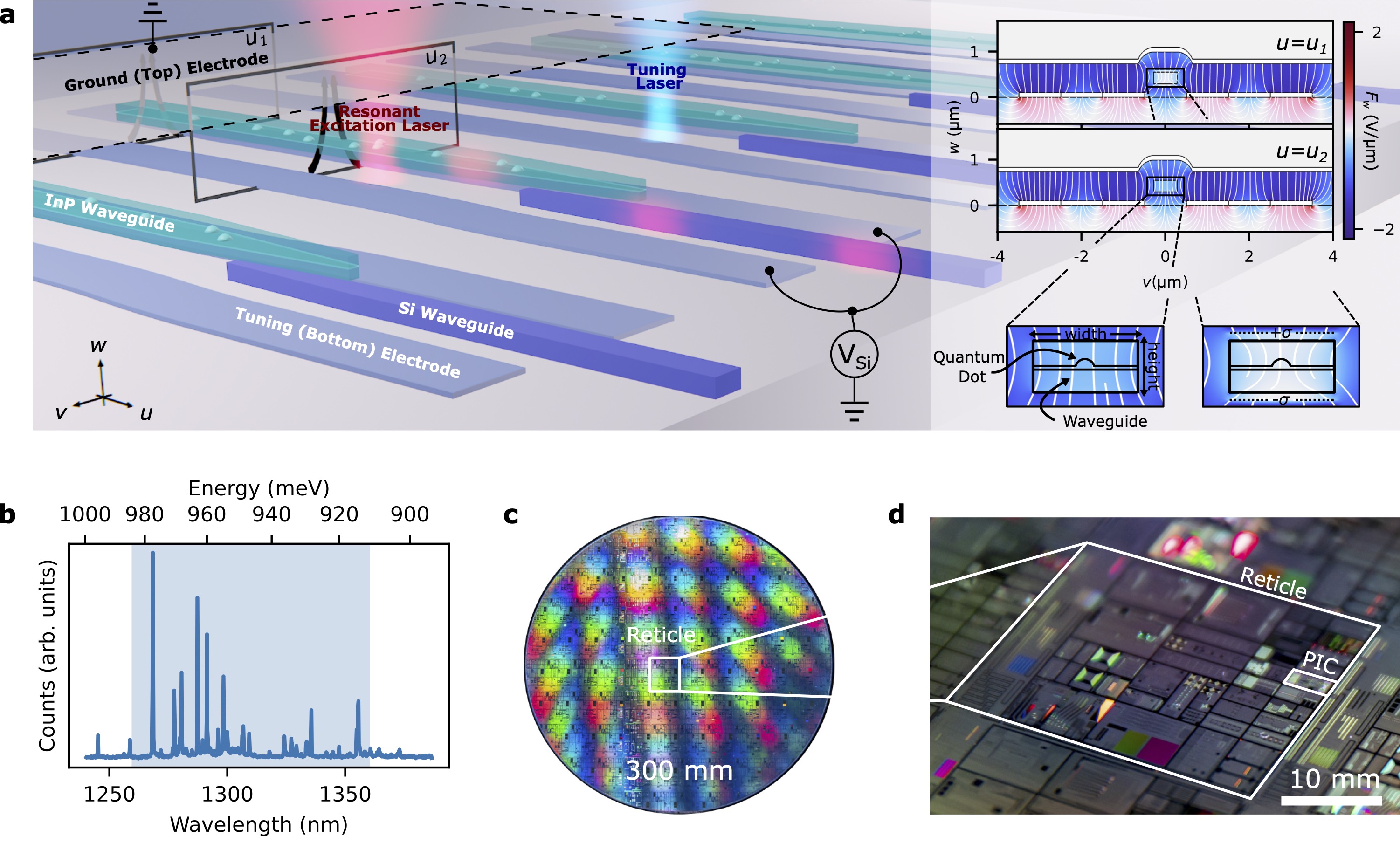
Hybrid architecture – Figure 1a illustrates our hybrid architecture, where we integrate the SOI PIC with InP waveguide chiplets containing a central layer of InAs/InP QDs. As shown in the inset, the segmented top and bottom electrodes enable the application of electric fields primarily perpendicular to the QD layer to tune exciton emission via the quantum confined Stark effect Miller et al. (1984, 1985). We realize these electrodes with segmented bottom electrodes in -doped Si and a top-deposited ground electrode.
Non-volatile memory Stark shift control – Spectrally tuning individual QDs along the waveguide direction, , would require complex control electronics while also placing extreme demands on this bottom electrode layer in terms of spatial resolution and wiring. Therefore, we implemented an entirely different approach to Stark shift control at individual QD locations: gate-controlled charge trapping of photogenerated carriers. Modeled by surface charges of () on the top (bottom) of the InP waveguide, these act as non-volatile floating gates that modulate the electric field across the QD layer, as seen by comparing the waveguide cross-sections at and in the inset of Fig. 1a.
Global telecom QD properties – We use confocal excitation to program the memory and pump the QDs. QD emission into an InP waveguide chiplet thereafter couples via adiabatically tapered inverse couplers to the SOI PIC’s waveguide layer for on-chip routing or edge-coupling into silica fibers for off-chip routing. Figure 1b plots a representative photoluminescence (PL) spectrum collected through the edge-couplers at a base temperature of 5 K and a pump laser wavelength nm at 0.5 µW focused to a µm spot-size. The spectrum shows QD emission in multiple, spectrally distinct lines in the telecom O-band; their density is consistent with 10 QDs µm-2.
Foundry PIC design & fabrication – We fabricated the PICs in the AIM Photonics’ foundry. Using 193 nm deep-ultraviolet water-immersion lithography, this fabrication process enables 300 mm wafer-scale production of SOI PICs with multiple metal and dielectric layers along with available - and -type doping. The PIC used an O-band specific process development kit element for broadband optical edge couplers featuring loss below 3 dB over a 1260-1360 nm wavelength range Timurdogan et al. (2019) and other components custom designed for O-band operation. Figure 1c shows a wafer before dicing. Figure 1d highlights the PIC in this study, which occupies a mm2 block of the reticle.
II.2 Hybrid Integration
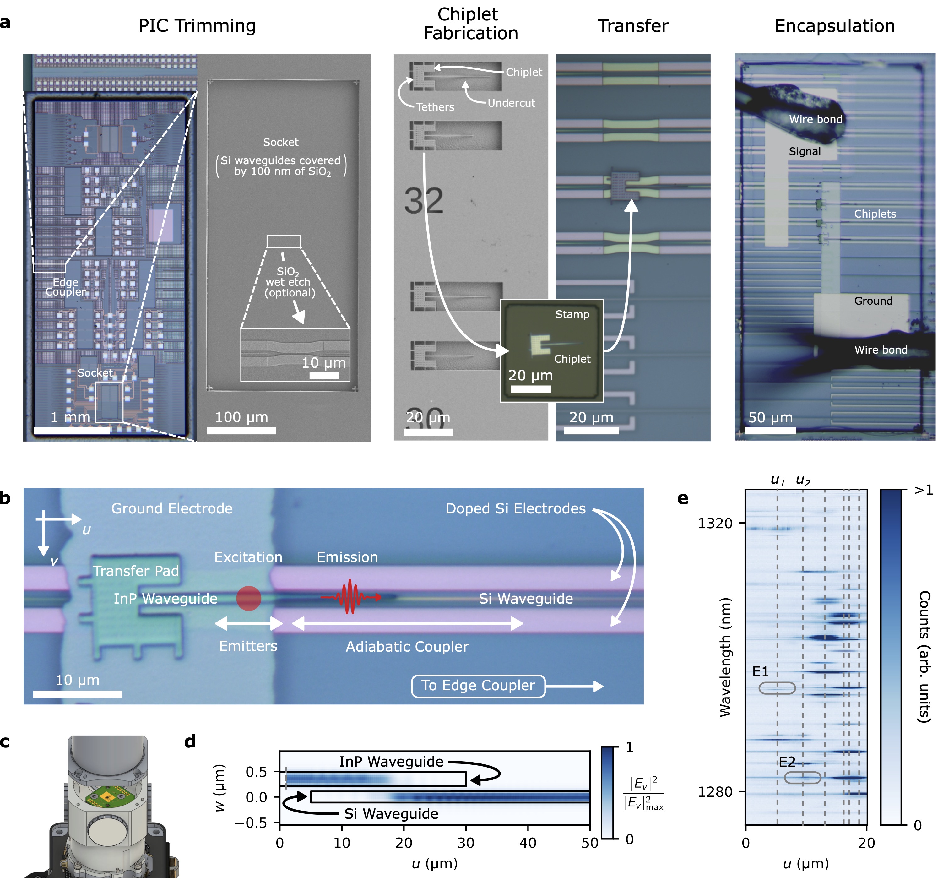
Postprocessing and chiplet integration – At this stage, all waveguides are still covered in oxide and metal layers, as required by the foundry. To integrate quantum devices, it was necessary to develop a series of post-processing steps suited for a university cleanroom. Starting from the foundry-provided PIC, Fig. 2a summarizes the key stages of postprocessing which begins with the fabrication of ‘quantum sockets’ from the PIC surface to the Si waveguides by optical lithography and wet etching. We leave a 100 nm oxide layer over the waveguides to ensure good mechanical adhesion and optical coupling between the chiplet and the PIC. In parallel, we fabricate suspended InP microchiplets with embedded InAs/InP QDs Lee et al. (2020) by electron beam lithography and a combination of dry and wet etching. We then proceed with transfer printing microchiplets from the parent InP chip into the PIC quantum sockets. This pick-and-place procedure uses a PDMS microstamp (50 µm x 50 µm) tracked under a microscope, achieving a chiplet placement accuracy of nm (see SI). Finally, in the ‘encapsulation’ step, we deposit a 475 nm thick PECVD oxide spacer layer and pattern a 20 nm Cr top electrode onto the quantum socket Aghaeimeibodi et al. (2019).
Figure 2b shows an integrated microchiplet at the end of the fabrication process. Here, the ground electrode covers the section of the nanobeam before the chiplet’s adiabatic taper. Our experiments target emitters between the ground and doped silicon electrodes as they strongly overlap with the electric field of this capacitive structure. After wirebonding to a cryo-compatible printed circuit board, we mount the PIC in a 5 K cryostat as illustrated in Fig. 2c. With a confocal microscope setup, we excite the QDs embedded in the InP chiplet through a window in the cryostat exposing the top of the device.
Chiplet to SOI waveguide coupling – The finite difference time domain simulation in Fig. 2d indicate that our optimized adiabatic couplers can reach a photon transfer efficiency of up to 99.5%. Fiber-to-fiber measurements through a 2 mm silicon waveguide with a gap bridged by a double-sided InP taper reveal that this adiabatic transfer can reach efficiencies of in practice. We extract this value by comparing transmission through the structure with transmission through a straight silicon waveguide. The latter measurement indicates a total transmission of while using 5 µm mode field diameter lensed fibers, indicating fiber-to-waveguide facet transmission better than 50% enabled by the multiple dielectric layers in this SOI PIC platform.
Low-temperature QD-PIC spectroscopy – Figure 2e presents a density plot of PL spectra under the same conditions as Fig. 1b, acquired while sweeping the excitation laser spot along the waveguide axis while collecting out of the PIC facet into a single mode fiber. This plot shows a number of distinct QD emission lines over a spatial extent of µm, which is consistent with the laser spot size. We will now consider detailed spectroscopy on emitters E1 and E2 at locations and .
II.3 Photon Statistics
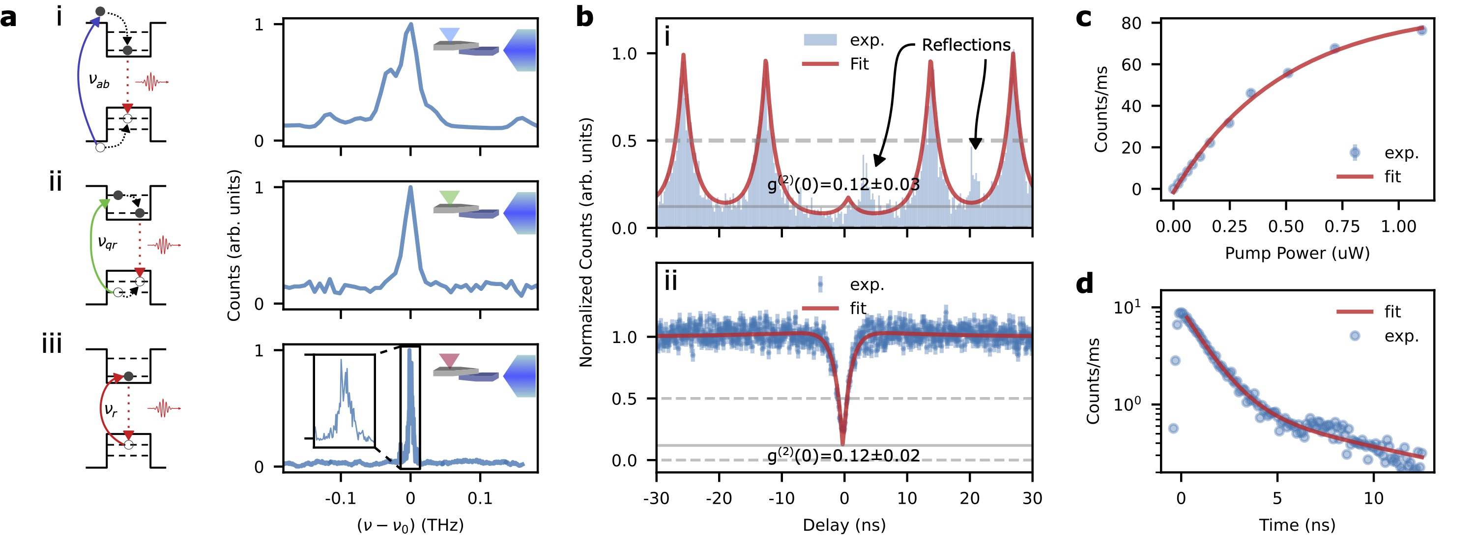
Photon statistics measurements - To demonstrate the versatility and performance of our system, we performed low-temperature photon correlation measurements on the PIC output facet under the three laser excitation regimes indicated in Fig. 3a: (i) above-band pumping, (ii) quasi-resonant excitation of a high-order excited state, and (iii) resonant excitation. The PL spectrum narrows to a linewidth of GHz when going from above-band to quasi-resonant excitation; this is near the 10 GHz resolution limit of the spectrometer that we use to measure (i) and (ii). Figure 3a(iii) shows the photoluminescence excitation obtained by scanning an external cavity diode 200 kHz linewidth laser across the emitter at a laser intensity of 10 µW/µm2 while measuring the PIC output with superconducting nanowire single photon detectors (SNSPDs). As seen from the inset, we estimate a linewidth of GHz. We found it unnecessary to use off-chip filtering under any excitation conditions during emission spectrum measurements, including the resonant case.
Next, we examine the purity of the excited photons with second order autocorrelation measurements using an off-chip Hanbury Brown-Twiss apparatus consisting of a 50:50 fiber splitter and SNSPDs. We first triggered above-band excitation with a pulsed 776 nm fiber-coupled laser with a 80 MHz repetition rate and a 120 fs pulse width. Figure 3b provides the resulting autocorrelation trace of the emitted photons after going through a 0.1 nm narrow-band tunable fiber filter that we use to remove residual counts from nearby emitters also excited by above-band pumping. In spite of spurious peaks resulting from imperfections in the exciting pulses (see SI), a fit of the data reveals clear anti-bunching at . Figure 3b also provides the result of similar measurements using a continuous wave tunable O-band laser resonantly exciting the emitter. The resonance fluorescence gives . This measurement did not require any filtering due to good pump rejection inherited from the perpendicular geometry of our excitation and collection optics Muller et al. (2007); Huber et al. (2020). Our normalized raw is similar to the value reported in other works that focus on collecting filter-free resonance fluorescence from visible QDs Huber et al. (2020). Fitting our autocorrelation data to a model incorporating our SNSPDs’ response time could imply a higher photon purity than what we obtain with our current fit. Additions to our measurement apparatus for improved photon purity through better pump rejection include polarization filtering Wang et al. (2019), temporal gating Reithmaier et al. (2015), or bi-chromatic pumping He et al. (2019).
Fitting the emitted photon flux against the pump intensity to indicates a saturation power of µW. These measurements are carried out with above-band excitation using an objective lens with a numerical aperture of 0.55, hence a saturation intensity of µW/µm2. We find that this power value varies from 0.14 µW to 0.57 µW based on measurements for five emitters (see SI). Figure 3c plots the saturation data and the corresponding fit for an emitter with a saturation power of µW.
Figure 3d plots the time-resolved PL under pulsed above-band excitation, as measured on the SNSPDs. Fitting to a double-exponential decay , where , gives ns, thereby suggesting a lifetime-limited linewidth of . We attribute and to bright excitons within well-defined QDs and adverse electron-hole recombination processes, respectively. Radiative decay traces for emitters with lower more prominently feature the influence of (see SI).
II.4 QD spectral tuning by a non-volatile memory
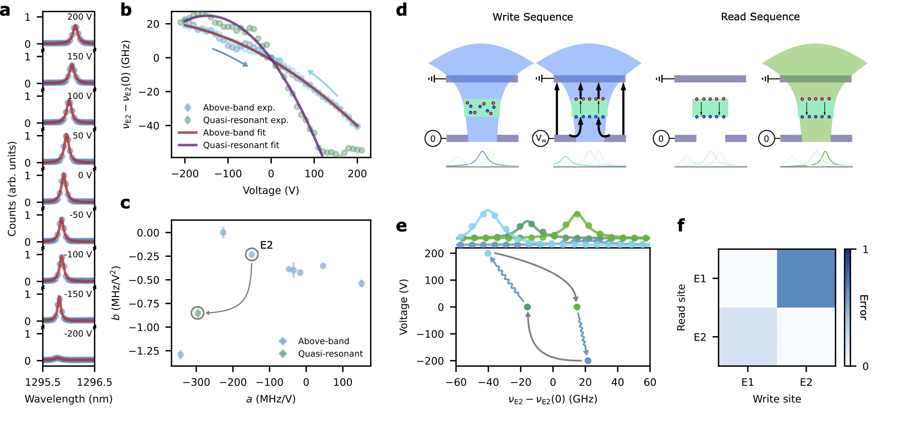
We quantify the tunability of our quantum socket by examining the PL spectra of emitter E2 under above-band excitation while increasing the voltage applied to the device. Figure 4a presents E2’s PL spectrum under continuous-wave (cw) above-band excitation as a function of the electric potential difference between the tuning electrodes and the ground-plane. As indicated in Fig. 1a, we expect this potential difference to apply a dominantly perpendicular electric field across the QDs. We observe a voltage-dependent shift in the emission line’s center frequency at an approximately constant PL intensity from V to V. We attribute the intensity drop at large negative potentials to local material variations, as each dot exhibits a different response (see SI). The PL linewidth and brightness is also approximately constant within roughly V. is also consistent up to the resolution of our spectrometer across multiple measurements, thus suggesting that our tuning mechanism does not induce any significant noise (see SI).
Figure 4b plots the detuning obtained from Lorentzian fits to the spectra from Fig. 4a. Fitting these data to a quadratic model gives a good agreement () for MHz/V and MHz/V2. Figure 4c provides the fitted and for E2 and seven other emitters in the transferred chiplets. We observe an average MHz/V, whereas the parameter falls around MHz/V2, indicating similar voltage sensitivities for our emitters.
The quadratic frequency shift with perpendicular electric field, agrees with the form of the quantum confined Stark effect:
| (1) | |||||
| (2) | |||||
| (3) | |||||
| (4) |
where and account for the dipole moment and the polarization of the dot, respectively. Here we introduce µm as a characteristic electrode spacing weighted by the fringing in the electric field as seen in Fig. 1a; the free variables and capture the reduction and offset of the electric field at the QD due to free carriers, respectively. Fitting this model with separately measured values of and Aghaeimeibodi et al. (2019) indicates that the strong electric field screening under above-band excitation () is improved under quasi-resonant excitation (). Both conditions entail a similar offset field of kV/cm and kV/cm, respectively.
To examine the role of charge distribution on the proposed screening, we proceed by applying a sequence of to the device under different illumination conditions. Figure 4d depicts the following steps of the sequence: write – illuminating the chiplet with above-band light while ramping from to a “write” value ; read – probing under quasi-resonant excitation. Figure 4e plots this write-read sequence for E2. Starting from probed under quasi-resonant excitation, program the dot to (. Likewise, programming the dot to (200 V,-40 GHz) under above-band illumination reverts the state of the dot back to . This shows the ability to write so that quasi-resonant excitation produces read values within 30 GHz. We attribute this memory effect to non-volatile charge redistribution near the QD.
To characterize the cross-talk of this non-volatile memory, we perform an illumination sequence from Figs. 4d,e on one dot, e.g. dot , followed by a measurement of the emission wavelength under quasi-resonant excitation. We then run an additional quasi-resonant measurement on a dot located µm away from the first one, e.g. dot . This procedure allows us to measure how changing the internal field applied to the one dot influences the internal field on the other. Specifically, for dot , we obtain the frequency shift by letting in Eq. (1), i.e.,
| (5) |
where is the initial internal field on dot and is the modification of this field following the above-band illumination of dot . Partial exposure to the optical field illuminating dot may cause a cross-talk on dot , i.e., . In practice, an aberrated illumination beam may cause such cross-talk. Even if completely mitigated, the diffraction limit will still lower-bound . We quantify the error from this cross-talk by , where is the Kronecker function. As seen from the cross-talk matrix in Fig. 4f, we observe a maximum cross-talk of 0.65 in the off-diagonals for emitters separated by roughly 5 µm.
III Discussion
Future work should consider the following approaches to increasing the spectral tuning range of our device, narrowing the emitter linewidth, and leveraging other capabilites of advanced SOI PIC platforms. Probing the emission of QDs between the transfer and encapsulation steps may provide insight into how the processing steps affect the coherence of the emitted photons. Such measurements would lead to an improved post-processing flow able to narrow the emission linewidths of the QDs, leading to charge reductions and a path towards widely-tunable and lifetime-limited on-chip SPEs at telecom wavelengths. Furthermore, modifying the design for charging a tuning component without direct contact to the transferred dots could provide a localized, non-volatile, and large-scale tuning mechanism for QDs with electrodes without altering the coherence or the tuning sensitivity of emitters. Inverting error matrices similar to the one in Fig. 4f could provide a means to mitigate cross-talk while tuning such emitters, hence enabling applications requiring multiple resonant SPEs.
The large-scale integration capabilities of silicon photonics make it ideally suited for hosting greater amounts of SPEs. Increasing the number of integrated chiplets would require a scalable transfer method, drawing on existing transfer printing techniques Meitl et al. (2006) used for large-scale hybrid integration of other light sources such as colloidal QDs and lasers Kim et al. (2011); Justice et al. (2012). Devices with large numbers of emitters could lead towards more sophisticated on-chip many-photon quantum systems that may also benefit from active components enabled by the platform such as RF electronics or cryogenics-compatible optical modulators Chakraborty et al. (2020). Integrating other components such as on-chip SNSPDs Ferrari et al. (2018); Gyger et al. (2021) could also enable more complex types of on-chip photonic computations, including more complex quantum information processing tasks Rudolph (2017) and machine learning Steinbrecher et al. (2019); Lopez-Pastor and Marquardt (2021).
A combination of QD positioning methods used during chiplet fabrication Liu et al. (2018); Schnauber et al. (2019) with large-scale schemes for optically probing nanophotonic structures Panuski et al. (2022) could efficiently prepare large numbers of QD chiplets for transfer. Preliminary screening of optical properties of emitters and improving their tunability beyond 100 GHz could lead towards on-chip sources spanning telecommunication windows.
In summary, we introduced a platform for integrating tunable single-photon emitters on large-scale PICs. By hybrid integration of InAs/InP chiplets with a state-of-the-art SOI PIC, we have demonstrated scalable emission wavelength programmability with individual emitter resolution. The excellent pump rejection of the PIC enables the observation of QD resonance fluorescence without additional filtering. The localized non-volatile spectral tuning opens the door to QD wavelength tuning at the scale of the number of resolvable laser spots, which can be in the millions with conventional microscopes. The combined control of photonic and atomic systems on a scalable platform enables a new generation of programmable quantum information processors manufactured in leading semiconductor foundries that can leverage many-body quantum systems.
Acknowledgements H.L. and D.E. acknowledge support from the NSF (1936314QII-TAQS) and AFOSR program FA9550-16-1-0391. H. L. acknowledges the support of the Natural Sciences and Engineering Research Council of Canada (NSERC), the National Science Foundation (NSF, Award no. ECCS-1933556), and of the QISE-NET program of the NSF (NSF award DMR-1747426). C.E-H. acknowledges funding from the European Union’s Horizon 2020 research and innovation program under the Marie Sklodowska-Curie grant agreement No.896401. M.A.B., S.H, C.-M.L., and E.W. acknowledge financial support from the National Science Foundation (grants #OMA1936314, #OMA2120757, #PHYS1915375, and #ECCS1933546), AFOSR (grant #FA23862014072), and the Maryland-ARL Quantum Partnership (W911NF1920181). The authors acknowledge James M. Daley for assisting with the sample’s fabrication along with Marco Colangelo, Alessandro Buzzi, and Camille Papon for useful discussions. The authors acknowledge MIT.nano’s facilities where additional fabrication work was performed. The simulations were performed using RSoft Photonic Device Tools distributed through Synospys’ University Software Program. The authors acknowledge X-Celeprint for distributing the PDMS stamps used in the assembly of the hybrid chip.
References
- He et al. (2013) Y.-M. He, Y. He, Y.-J. Wei, D. Wu, M. Atatüre, C. Schneider, S. Höfling, M. Kamp, C.-Y. Lu, and J.-W. Pan, Nat. Nanotechnol. 8, 213 (2013).
- Somaschi et al. (2016) N. Somaschi, V. Giesz, L. De Santis, J. C. Loredo, M. P. Almeida, G. Hornecker, S. L. Portalupi, T. Grange, C. Antón, J. Demory, C. Gómez, I. Sagnes, N. D. Lanzillotti-Kimura, A. Lemaítre, A. Auffeves, A. G. White, L. Lanco, and P. Senellart, Nat. Photon. 10, 340 (2016).
- Ding et al. (2016) X. Ding, Y. He, Z.-C. Duan, N. Gregersen, M.-C. Chen, S. Unsleber, S. Maier, C. Schneider, M. Kamp, S. Höfling, C.-Y. Lu, and J.-W. Pan, Phys. Rev. Lett. 116, 020401 (2016).
- Wang et al. (2019) H. Wang, Y.-M. He, T. H. Chung, H. Hu, Y. Yu, S. Chen, X. Ding, M. C. Chen, J. Qin, X. Yang, R.-Z. Liu, Z. C. Duan, J. P. Li, S. Gerhardt, K. Winkler, J. Jurkat, L.-J. Wang, N. Gregersen, Y.-H. Huo, Q. Dai, S. Yu, S. Höfling, C.-Y. Lu, and J.-W. Pan, Nat. Photon. 13, 770 (2019).
- Senellart et al. (2017) P. Senellart, G. Solomon, and A. White, Nat. Nanotechnol. 12, 1026 (2017).
- Tomm et al. (2021) N. Tomm, A. Javadi, N. O. Antoniadis, D. Najer, M. C. Löbl, A. R. Korsch, R. Schott, S. R. Valentin, A. D. Wieck, A. Ludwig, and R. J. Warburton, Nat. Nanotechnol. 16, 399 (2021).
- Thomas et al. (2021) S. E. Thomas, M. Billard, N. Coste, S. C. Wein, Priya, H. Ollivier, O. Krebs, L. Tazaïrt, A. Harouri, A. Lemaitre, I. Sagnes, C. Anton, L. Lanco, N. Somaschi, J. C. Loredo, and P. Senellart, Phys. Rev. Lett. 126, 233601 (2021).
- Dousse et al. (2010) A. Dousse, J. Suffczyński, A. Beveratos, O. Krebs, A. Lemaître, I. Sagnes, J. Bloch, P. Voisin, and P. Senellart, Nature 466, 217 (2010).
- Müller et al. (2014) M. Müller, S. Bounouar, K. D. Jöns, M. Glässl, and P. Michler, Nat. Photon. 8, 224 (2014).
- Liu et al. (2019) J. Liu, R. Su, Y. Wei, B. Yao, S. F. C. d. Silva, Y. Yu, J. Iles-Smith, K. Srinivasan, A. Rastelli, J. Li, and X. Wang, Nat. Nanotechnol. 14, 586 (2019).
- Javadi et al. (2015) A. Javadi, I. Söllner, M. Arcari, S. L. Hansen, L. Midolo, S. Mahmoodian, G. Kiršanskė, T. Pregnolato, E. H. Lee, J. D. Song, S. Stobbe, and P. Lodahl, Nat. Commun. 6, 8655 (2015).
- Le Jeannic et al. (2021) H. Le Jeannic, T. Ramos, S. F. Simonsen, T. Pregnolato, Z. Liu, R. Schott, A. D. Wieck, A. Ludwig, N. Rotenberg, J. J. García-Ripoll, and P. Lodahl, Phys. Rev. Lett. 126, 023603 (2021).
- Le Jeannic et al. (2022) H. Le Jeannic, A. Tiranov, J. Carolan, T. Ramos, Y. Wang, M. H. Appel, S. Scholz, A. D. Wieck, A. Ludwig, N. Rotenberg, L. Midolo, J. J. García-Ripoll, A. S. Sørensen, and P. Lodahl, Nat. Phys. 18, 1191 (2022).
- Lindner and Rudolph (2009) N. H. Lindner and T. Rudolph, Phys. Rev. Lett. 103, 113602 (2009).
- Schwartz et al. (2016) I. Schwartz, D. Cogan, E. R. Schmidgall, Y. Don, L. Gantz, O. Kenneth, N. H. Lindner, and D. Gershoni, Science 354, 434 (2016).
- Istrati et al. (2020) D. Istrati, Y. Pilnyak, J. C. Loredo, C. Antón, N. Somaschi, P. Hilaire, H. Ollivier, M. Esmann, L. Cohen, L. Vidro, C. Millet, A. Lemaître, I. Sagnes, A. Harouri, L. Lanco, P. Senellart, and H. S. Eisenberg, Nat. Commun. 11, 5501 (2020).
- Cogan et al. (2023) D. Cogan, Z.-E. Su, O. Kenneth, and D. Gershoni, Nature Photonics 17, 324 (2023).
- Stockill et al. (2016) R. Stockill, C. Le Gall, C. Matthiesen, L. Huthmacher, E. Clarke, M. Hugues, and M. Atatüre, Nat. Commun. 7, 12745 (2016).
- Gangloff et al. (2019) D. Gangloff, G. Ethier-Majcher, C. Lang, E. Denning, J. Bodey, D. Jackson, E. Clarke, M. Hugues, C. Le Gall, and M. Atatüre, Science 364, 62 (2019).
- Gangloff et al. (2021) D. A. Gangloff, L. Zaporski, J. H. Bodey, C. Bachorz, D. M. Jackson, G. Éthier-Majcher, C. Lang, E. Clarke, M. Hugues, C. Le Gall, and M. Atatüre, Nat. Phys. 17, 1247 (2021).
- Zaporski et al. (2023) L. Zaporski, N. Shofer, J. H. Bodey, S. Manna, G. Gillard, M. H. Appel, C. Schimpf, S. F. Covre da Silva, J. Jarman, G. Delamare, G. Park, U. Haeusler, E. A. Chekhovich, A. Rastelli, D. A. Gangloff, M. Atatüre, and C. Le Gall, Nature Nanotechnology 18, 257 (2023).
- Dietrich et al. (2016) C. P. Dietrich, A. Fiore, M. G. Thompson, M. Kamp, and S. Höfling, Laser Photon. Rev. 10, 870 (2016).
- Lodahl (2018) P. Lodahl, Quantum Sci. Technol. 3, 013001 (2018).
- Grim et al. (2019) J. Q. Grim, A. S. Bracker, M. Zalalutdinov, S. G. Carter, A. C. Kozen, M. Kim, C. S. Kim, J. T. Mlack, M. Yakes, B. Lee, et al., Nat. Mater. 18, 963 (2019).
- Papon et al. (2022) C. Papon, Y. Wang, R. Uppu, S. Scholz, A. D. Wieck, A. Ludwig, P. Lodahl, and L. Midolo, , Preprint at https://arxiv.org/abs/2210.09826 (2022).
- Tiranov et al. (2023) A. Tiranov, V. Angelopoulou, C. J. van Diepen, B. Schrinski, O. A. D. Sandberg, Y. Wang, L. Midolo, S. Scholz, A. D. Wieck, A. Ludwig, et al., Science 379, 389 (2023).
- Jöns et al. (2015) K. D. Jöns, U. Rengstl, M. Oster, F. Hargart, M. Heldmaier, S. Bounouar, S. M. Ulrich, M. Jetter, and P. Michler, J. Phys. D: Appl. Phys 48, 085101 (2015).
- Kim et al. (2020) J.-H. Kim, S. Aghaeimeibodi, J. Carolan, D. Englund, and E. Waks, Optica 7, 291 (2020).
- Elshaari et al. (2020) A. W. Elshaari, W. Pernice, K. Srinivasan, O. Benson, and V. Zwiller, Nat. Photon. 14, 285 (2020).
- Kim et al. (2017) J.-H. Kim, S. Aghaeimeibodi, C. J. Richardson, R. P. Leavitt, D. Englund, and E. Waks, Nano Lett. 17, 7394 (2017).
- Katsumi et al. (2019) R. Katsumi, Y. Ota, A. Osada, T. Yamaguchi, T. Tajiri, M. Kakuda, S. Iwamoto, H. Akiyama, and Y. Arakawa, APL Photonics 4, 036105 (2019).
- Katsumi et al. (2020) R. Katsumi, Y. Ota, A. Osada, T. Tajiri, T. Yamaguchi, M. Kakuda, S. Iwamoto, H. Akiyama, and Y. Arakawa, Appl. Phys. Lett. 116, 041103 (2020).
- Mouradian et al. (2015) S. L. Mouradian, T. Schröder, C. B. Poitras, L. Li, J. Goldstein, E. H. Chen, M. Walsh, J. Cardenas, M. L. Markham, D. J. Twitchen, M. Lipson, and D. Englund, Phys. Rev. X 5, 031009 (2015).
- Zadeh et al. (2016) I. E. Zadeh, A. W. Elshaari, K. D. Jöns, A. Fognini, D. Dalacu, P. J. Poole, M. E. Reimer, and V. Zwiller, Nano Lett. 16, 2289 (2016) .
- Elshaari et al. (2017) A. W. Elshaari, I. E. Zadeh, A. Fognini, M. E. Reimer, D. Dalacu, P. J. Poole, V. Zwiller, and K. D. Jöns, Nat. Commun. 8, 379 (2017) .
- Davanco et al. (2017) M. Davanco, J. Liu, L. Sapienza, C.-Z. Zhang, J. De Miranda Cardoso, V. Verma, R. Mirin, S. W. Nam, L. Liu, and K. Srinivasan, Nat. Commun. 8, 889 (2017).
- Elshaari et al. (2018) A. W. Elshaari, E. Büyüközer, I. E. Zadeh, T. Lettner, P. Zhao, E. Schöll, S. Gyger, M. E. Reimer, D. Dalacu, P. J. Poole, et al., Nano Lett. 18, 7969 (2018).
- Chanana et al. (2022) A. Chanana, H. Larocque, R. Moreira, J. Carolan, B. Guha, E. G. Melo, V. Anant, J. Song, D. Englund, D. J. Blumenthal, K. Srinivasan, and M. Davanco, Nat. Commun. 13, 7693 (2022).
- Sun et al. (2013) J. Sun, E. Timurdogan, A. Yaacobi, E. S. Hosseini, and M. R. Watts, Nature 493, 195 (2013).
- Bogaerts et al. (2020a) W. Bogaerts, D. Pérez, J. Capmany, D. A. Miller, J. Poon, D. Englund, F. Morichetti, and A. Melloni, Nature 586, 207 (2020a).
- Bogaerts et al. (2020b) W. Bogaerts, H. Sattari, P. Edinger, A. Y. Takabayashi, I. Zand, X. Wang, A. Ribeiro, M. Jezzini, C. Errando-Herranz, G. Talli, et al., in Silicon Photonics XV, Vol. 11285 (SPIE, 2020) p. 1128503.
- Edinger et al. (2021) P. Edinger, A. Y. Takabayashi, C. Errando-Herranz, U. Khan, H. Sattari, P. Verheyen, W. Bogaerts, N. Quack, and K. B. Gylfason, Opt. Lett. 46, 5671 (2021).
- Miller et al. (1984) D. A. B. Miller, D. S. Chemla, T. C. Damen, A. C. Gossard, W. Wiegmann, T. H. Wood, and C. A. Burrus, Phys. Rev. Lett. 53, 2173 (1984).
- Miller et al. (1985) D. A. B. Miller, D. S. Chemla, T. C. Damen, A. C. Gossard, W. Wiegmann, T. H. Wood, and C. A. Burrus, Phys. Rev. B 32, 1043 (1985).
- Timurdogan et al. (2019) E. Timurdogan, Z. Su, R.-J. Shiue, C. V. Poulton, M. J. Byrd, S. Xin, and M. R. Watts, in Optical Fiber Communication Conference (OFC) 2019 (Optica Publishing Group, 2019) p. Tu2A.1.
- Lee et al. (2020) C.-M. Lee, M. A. Buyukkaya, S. Harper, S. Aghaeimeibodi, C. J. Richardson, and E. Waks, Nano Lett. 21, 323 (2020).
- Aghaeimeibodi et al. (2019) S. Aghaeimeibodi, C.-M. Lee, M. A. Buyukkaya, C. J. Richardson, and E. Waks, Appl. Phys. Lett. 114, 071105 (2019).
- Muller et al. (2007) A. Muller, E. B. Flagg, P. Bianucci, X. Y. Wang, D. G. Deppe, W. Ma, J. Zhang, G. J. Salamo, M. Xiao, and C. K. Shih, Phys. Rev. Lett. 99, 187402 (2007).
- Huber et al. (2020) T. Huber, M. Davanco, M. Müller, Y. Shuai, O. Gazzano, and G. S. Solomon, Optica 7, 380 (2020).
- Reithmaier et al. (2015) G. Reithmaier, M. Kaniber, F. Flassig, S. Lichtmannecker, K. Müller, A. Andrejew, J. Vuckovic, R. Gross, and J. Finley, Nano Lett. 15, 5208 (2015).
- He et al. (2019) Y.-M. He, H. Wang, C. Wang, M. C. Chen, X. Ding, J. Qin, Z. C. Duan, S. Chen, J. P. Li, R.-Z. Liu, C. Schneider, M. Atatüre, S. Höfling, C.-Y. Lu, and J.-W. Pan, Nat. Phys. 15, 941 (2019).
- Meitl et al. (2006) M. A. Meitl, Z.-T. Zhu, V. Kumar, K. J. Lee, X. Feng, Y. Y. Huang, I. Adesida, R. G. Nuzzo, and J. A. Rogers, Nat. Mater. 5, 33 (2006).
- Kim et al. (2011) T.-H. Kim, K.-S. Cho, E. K. Lee, S. J. Lee, J. Chae, J. W. Kim, D. H. Kim, J.-Y. Kwon, G. Amaratunga, S. Y. Lee, B. L. Choi, Y. Kuk, J. M. Kim, and K. Kim, Nat. Photon. 5, 176 (2011).
- Justice et al. (2012) J. Justice, C. Bower, M. Meitl, M. B. Mooney, M. A. Gubbins, and B. Corbett, Nat. Photon. 6, 610 (2012).
- Chakraborty et al. (2020) U. Chakraborty, J. Carolan, G. Clark, D. Bunandar, G. Gilbert, J. Notaros, M. R. Watts, and D. R. Englund, Optica 7, 1385 (2020).
- Ferrari et al. (2018) S. Ferrari, C. Schuck, and W. Pernice, Nanophotonics 7, 1725 (2018).
- Gyger et al. (2021) S. Gyger, J. Zichi, L. Schweickert, A. W. Elshaari, S. Steinhauer, S. F. Covre da Silva, A. Rastelli, V. Zwiller, K. D. Jöns, and C. Errando-Herranz, Nat. Commun. 12, 1408 (2021).
- Rudolph (2017) T. Rudolph, APL Photonics 2, 030901 (2017).
- Steinbrecher et al. (2019) G. R. Steinbrecher, J. P. Olson, D. Englund, and J. Carolan, npj Quantum Inf. 5, 60 (2019).
- Lopez-Pastor and Marquardt (2021) V. Lopez-Pastor and F. Marquardt, , Preprint at https://arxiv.org/abs/2103.04992 (2021).
- Liu et al. (2018) J. Liu, K. Konthasinghe, M. Davanço, J. Lawall, V. Anant, V. Verma, R. Mirin, S. W. Nam, J. D. Song, B. Ma, Z. S. Chen, H. Q. Ni, Z. C. Niu, and K. Srinivasan, Phys. Rev. Appl. 9, 064019 (2018).
- Schnauber et al. (2019) P. Schnauber, A. Singh, J. Schall, S. I. Park, J. D. Song, S. Rodt, K. Srinivasan, S. Reitzenstein, and M. Davanco, Nano Lett. 19, 7164 (2019).
- Panuski et al. (2022) C. L. Panuski, I. Christen, M. Minkov, C. J. Brabec, S. Trajtenberg-Mills, A. D. Griffiths, J. J. D. McKendry, G. L. Leake, D. J. Coleman, C. Tran, J. St Louis, J. Mucci, C. Horvath, J. N. Westwood-Bachman, S. F. Preble, M. D. Dawson, M. J. Strain, M. L. Fanto, and D. R. Englund, Nat. Photon. 16, 834 (2022).