Improved Coherence in Optically-Defined Niobium Trilayer Junction Qubits
Abstract
Niobium offers the benefit of increased operating temperatures and frequencies for Josephson junctions, which are the core component of superconducting devices. However existing niobium processes are limited by more complicated fabrication methods and higher losses than now-standard aluminum junctions. Combining recent trilayer fabrication advancements, methods to remove lossy dielectrics and modern superconducting qubit design, we revisit niobium trilayer junctions and fabricate all-niobium transmons using only optical lithography. We characterize devices in the microwave domain, measuring coherence times up to \qty62 and an average qubit quality factor above : much closer to state-of-the-art aluminum-junction devices. We find the higher superconducting gap energy also results in reduced quasiparticle sensitivity above \qty0.16, where aluminum junction performance deteriorates. Our low-loss junction process is readily applied to standard optical-based foundry processes, opening new avenues for direct integration and scalability, and paves the way for higher-temperature and higher-frequency quantum devices.
A wide variety of superconducting devices have developed on the basis of Josephson junctions: their applications range from quantum-limited amplification and metrology [1, 2, 3] to digital logic [4, 5, 6] and they are an attractive platform for scalable quantum computing architectures due to their design flexibility and wide range of coupling strengths. Increasingly complex and robust quantum circuits have been demonstrated with aluminum junctions [7], however niobium is a tantalizing alternative superconductor due to its larger energy gap (and thus higher critical temperature and pair-breaking photon frequency) [8]. Taking advantage of this wider operating regime, niobium trilayer Josephson junctions became standard for single-flux-quantum circuits operating at liquid helium temperatures [4, 5, 6]. Employing these well-established fabrication processes, some early implementations of superconducting qubits were developed with niobium junctions [9, 10, 11, 12, 13, 14, 15, 16]. However, these initial niobium qubits only retained quantum state coherence for less than \qty400, diminished by coupling to sources of dephasing and dissipation in the junction and the qubit environment.
Minimizing these loss sources is crucial in all sensitive quantum systems, but particularly for qubits, which must remain coherent over the duration of many gate operations. Significant effort has since been dedicated to investigating and reducing sources of decoherence [17], demanding either adjustments of circuit geometry to limit or dilute coupling to spurious channels, or reducing the use of lossy amorphous dielectric materials. The need for insulated wiring contacts in these niobium trilayer junctions required growing passivating amorphous dielectric material in direct contact with the junction barrier, which likely degraded early qubit coherence [18], and limited their use in quantum devices. Higher temperature junctions with low loss promise a transformative source of strong nonlinearity for high-frequency quantum devices [19, 20], and have since seen renewed interest from efforts to integrate digital and quantum logic [21, 22, 23], and the exploration of tunnel barrier materials beyond the limitations of aluminum [24, 25, 26]. Notably, by removing amorphous insulating scaffolding and increasing the circuit volume to reduce junction participation, qubits with epitaxially grown NbN junctions with crystalline AlN barriers have increased coherence times to \qty16 [27]. We apply similar improvements to traditional Nb/Al/AlOx processes, which are attractive due to the simpler deposition methods required.
In this letter, we use an improved fabrication method to revisit niobium trilayer junctions as the core component of transmon qubits and explore their coherence properties. We describe a method to form a temporary self-aligned sidewall-passivating spacer structure based on Ref. [28], which limits the amorphous spacer material to the smallest necessary region, and can later be chemically removed to further reduce dielectric loss. We find that high-temperature spacer growth methods greatly reduce the critical current density of the junction barrier, allowing us to utilize exclusively optical lithography to fabricate high-nonlinearity junctions for microwave qubits. We find that our all-niobium qubits have lifetimes as high as \qty62 with an average qubit quality factor of : much closer to state-of-the-art qubits than past Nb/Al/AlOx devices [9, 10, 11, 12, 13, 14]. We further observe that the higher superconducting gap energy results in reduced sensitivity to quasiparticles, particularly above \qty160\milli, where conventional aluminum-junction qubit performance deteriorates. These results demonstrate the reemergent relevance of niobium junctions for pushing the boundaries of superconducting devices.
Despite niobium’s attractive electrical properties, in thin layers its oxides are imperfect insulators with high dielectric loss [18], resulting in very poor natural tunnel junction barriers. Aluminum, on the other hand, forms a thin self-terminating oxide with low leakage and loss, but has a low critical temperature. The trilayer method leverages the strengths of both of these materials by using a thin layer of oxidized aluminum as the tunnel barrier and encapsulating it with niobium: through the proximity effect the Josephson junction inherits desired electrical properties and a clean tunnel barrier. This trilayer structure is typically grown on a wafer-scale as the first step in fabrication, enabling excellent uniformity [29, 30] and high purity growth methods.
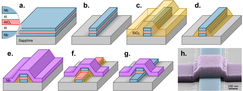
Our fabrication process (see Appendix A) is illustrated in Fig. 1. Similar to methods using sputtering, our trilayer is formed in a shadow-evaporation-compatible electron-beam system by depositing \qty80 of Nb and \qty8 of Al on high-purity single-crystal sapphire that has been annealed and chemically etched to remove surface damage. The deposition rate is kept high to maximize film quality (see Appendix B). To reduce defects and promote aluminum oxide formation [31], the aluminum is first ion milled then oxidized with an \ceO2-\ceAr mixture. To prevent oxygen diffusion into the Nb layer and the formation of lossy \ceNbO_x [32, 18], the oxidized Al surface is protected by a thin (\qty3) capping layer of Al. This layer is deposited while rotating the substrate at an angle for complete coverage while keeping it thin enough to avoid affecting junction properties. A (\qty150) thick counter electrode is then deposited on top, forming the trilayer in-situ, without breaking vacuum.
The trilayer is patterned with I-line 111exposed with a \qty375 laser photolithography and plasma-etched in one step with \ceCl2, \ceBCl3 and \ceAr to define the bottom electrode (Fig. 1b). As it is necessary to make contact to the counter electrode without touching the base electrode, we then form an insulating sidewall-passivating spacer structure [28]. Amorphous \ceSiO2 is grown isotropically (Fig. 1c) by either plasma-enhanced chemical vapor deposition (PECVD) which heats the wafer to \qty300 for \qty16min or high density plasma-enhanced chemical vapor deposition (HDPCVD) (\qty90). The \ceSiO2 is now etched anisotropically with a highly directional \ceCF4, \ceCHF3 and \ceAr plasma, which forms the spacer structure when the bulk material has been etched away (Fig. 1d). The contaminated trilayer surface is ion milled, and the \qty160 Nb wiring layer is electron-beam-deposited on the sample (Fig. 1e). We verify that this forms a low-resistance contact to the counter electrode (see Appendix B).
The wiring layer is patterned and a selective \ceSF6, \ceCHF3, \ceO2 and \ceAr plasma etch removes the wiring layer and the counter electrode, defining the perpendicular top junction electrode (Fig. 1f). This etch is carefully optimized to minimize the formation of lossy fluorocarbon polymers [34] (see Appendix C) while preserving chemical selectivity: and although the plasma etches the Al layers far slower than Nb, the etch is still timed to finish a few seconds after the counter electrode is fully removed to limit excessive polymer deposition. Finally, to further remove the lossy amorphous materials present in the junction, a solution of \ceNH4F and acetic acid 222Transene AlPAD Etch 639 are used to dissolve the remaining \ceSiO2: this process additionally removes any exposed Al and a small amount of surface \ceNbO_x (Fig. 1g). As this step can dissolve aluminum in the junction as well, etch times are kept below \qty15. This final treatment could likely be improved with a \ceHF vapor etch, which has shown good results forming similar contact structures [36].
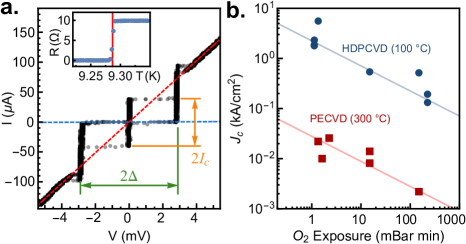
We verify the expected Josephson junction behavior [37] in our devices by measuring their hysteretic current-voltage curves in Fig. 2a. When cooled to \qty860\milli, the un-shunted junction shows a zero-resistance superconducting branch up to the critical current , and an energy gap , corresponding to a critical temperature , in agreement with the transition temperature seen in resistivity measurements. Measuring the asymptotic normal state resistance above the energy gap we find a product of \qty1.5\milli, similar to values reported previously for Nb trilayer junctions [38, 28, 39, 29, 30]. Although measurements of the subgap region were limited by the experiment hardware, no excessive subgap leakage currents are observed.
Using the product found above, we can use room-temperature junction resistances to predict low-temperature properties [40, 41]. Fitting the measured resistance for junctions of varying areas with two free parameters, specific resistivity and junction critical dimension bias (see Appendix D), we obtain the effective junction areas and the specific critical current density for each wafer. This method allows us to easily investigate effects of the fabrication process on junction electrical parameters. For Nb trilayers, the critical current density is sensitive to temperature [38] as well as oxygen exposure , the product of oxygen partial pressure and oxidation time: this relationship has been empirically found to match [38, 42, 28, 43, 44]. In Fig. 2b we plot as a function of for wafers with trilayers grown using various oxidation parameters and fabricated with two spacer deposition methods. For the HDPCVD junctions, we find critical current densities in the \unit\kilo\per\squared range, comparable with other methods [28, 45, 38, 39], and observe reasonable agreement with the oxygen exposure dependence described above. The effect of process temperature is readily apparent when we examine junctions with high-temperature-grown PECVD spacers: compared to HDPCVD junctions, we observe nearly a factor of 50 reduction in . We find this temperature-annealing effect activates above \qty200 (see Appendix E), in agreement with [38], and is likely the result of reduced barrier transparency [46] from diffusion.
With access to wide ranges of , we can use PECVD-annealed junctions to realize qubit junctions with optical lithography. We fabricate microwave transmon qubits [47, 48] with a standard geometry (see Appendix F) capacitively coupled to a coplanar waveguide resonator for dispersive readout. The qubit capacitor, ground plane and readout resonator are defined on either the base electrode or wiring layer, so no additional fabrication steps are needed. Chips with several qubits and their readout resonators sharing a common microwave feedline are characterized at the base stage of a dilution refrigerator (\qtyrange[range-units = single,range-phrase = –]4595\milli). Using microwave spectroscopy [47] we verify our qubits have anharmonicities around \qty140, and couple with strengths of \qtyrange[range-units = single,range-phrase = –]3060 to their readout resonators.
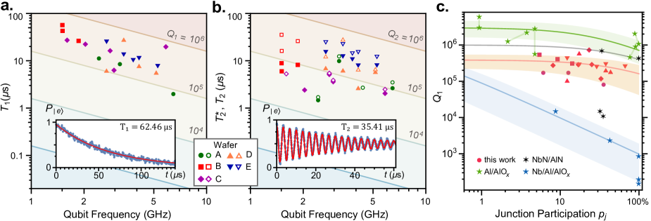
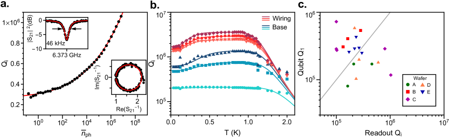
For superconducting qubits, the relaxation time and dephasing time are parameters of particular interest, as they dictate qubit limitations and act as sensitive probes for loss channels. We measure relaxation time by placing each qubit in its excited state and measuring it after time : fitting the exponential decay gives the characteristic time . We perform these measurements for each qubit and show averaged results as a function of qubit frequency in Fig. 3a, finding for our best device. To probe loss channels in detail we use the frequency-independent qubit quality factor , which we find for our devices is on average above : within an order of magnitude of recent aluminum qubits [49, 50, 51, 52, 7] and similar to readout resonator quality factors (see Appendix G). We also perform a Ramsey experiment to measure the dephasing time , and a Hahn-echo experiment to characterize the spin-echo dephasing time . We find that is within a factor of 2 of , and particularly limited at lower qubit frequencies, where the environment two level system (TLS) temperature is higher and system noise is higher. The values, which decouple low frequency noise are noticeably higher, demonstrated in particular by the qubits below \qty2 from wafer B, suggesting that more careful filtering and environment control could reduce dephasing further.
To assess loss contributions from the junction independent of other sources, in Fig. 3c we use the increased junction participation ratio [49, 53] in our devices to examine the effects on . For our devices (red), we estimate an effective junction quality factor of : approximately 100 times greater than previous Nb/Al/ qubits (blue) [9, 10, 11, 12, 13, 14, 15, 16], and much closer to epitaxial NbN junctions (black) [25, 26, 27] and modern aluminum-junction qubits (green) [51, 52, 50, 49]. Extrapolating to lower values, we find our device loss is largely not limited by the junction, indicating that material refinements and device engineering could further improve qubit performance.
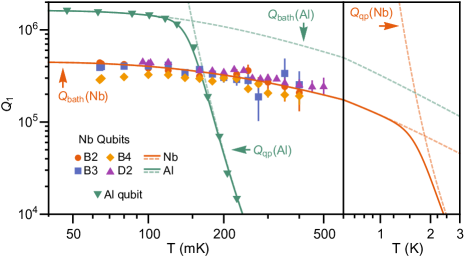
Next we investigate our qubits at increased operating temperatures, shown in Fig 4. We observe a mild decrease in with temperature above 160 mK, consistent with heating from the environment bath [14], but importantly don’t see the drastic temperature dependence expected for quasiparticle-induced loss [54], in line with expectations for niobium. The advantage of higher-temperature junctions is apparent when comparing our qubit performance to an aluminum counterpart: above \qty160\milli, the aluminum qubit is quickly overwhelmed with quasiparticle-induced decoherence, whereas our devices largely retain their properties.
We have described a Nb/Al//Al/Nb trilayer fabrication method demonstrating a 100-fold improvement in junction loss at the single-photon level. By removing lossy dielectric materials wherever possible, we use our low current density junction process to fabricate microwave transmon qubits using I-line photolithography demonstrating qubit quality factors within an order of magnitude of recent aluminum devices. Our qubits have relatively high junction participation ratios, which could either be reduced to improve coherence through material optimization [18], or exploited further to significantly reduce qubit size [24, 49]. Together with this device footprint flexibility, our all-optical qubit process opens the door to large-scale direct integration of scalable quantum processors with digital superconducting logic [21, 22, 23]. Niobium’s higher energy gap significantly reduces sensitivity to quasiparticles for our junctions compared to aluminum analogues, allowing operation at much higher frequencies, and resulting in far less decoherence above \qty160\milli where conventional qubit properties deteriorate. Combined with their low loss, these properties make our trilayer junctions a promising candidate for quantum architectures with lower cooling power requirements, hybrid qubit systems requiring elevated temperatures, and enable new possibilities for nonlinear elements at millimeter-wave frequencies [19, 20], paving the way for higher temperature, higher frequency quantum devices.
The authors thank P. Duda and J. Martinez for assistance with fabrication development, and S. Anferov for assistance with air-free techniques. This work is supported by the U.S. Department of Energy Office of Science National Quantum Information Science Research Centers as part of the Q-NEXT center, and partially supported by the University of Chicago Materials Research Science and Engineering Center, which is funded by the National Science Foundation under Grant No. DMR-1420709. This work made use of the Pritzker Nanofabrication Facility of the Institute for Molecular Engineering at the University of Chicago, which receives support from Soft and Hybrid Nanotechnology Experimental (SHyNE) Resource (NSF ECCS-2025633).
References
- Jeanneret and Benz [2009] B. Jeanneret and S. Benz, Application of the josephson effect in electrical metrology, The European Physical Journal Special Topics 172, 181 (2009).
- Vijay et al. [2009] R. Vijay, M. Devoret, and I. Siddiqi, Invited review article: The josephson bifurcation amplifier, Review of Scientific Instruments 80, 111101 (2009).
- Braginski [2019] A. I. Braginski, Superconductor electronics: Status and outlook, Journal of superconductivity and novel magnetism 32, 23 (2019).
- Vernik et al. [2017] I. V. Vernik, A. F. Kirichenko, O. A. Mukhanov, and T. A. Ohki, Energy-efficient and compact ersfq decoder for cryogenic ram, IEEE Transactions on Applied Superconductivity 27, 1 (2017).
- Likharev and Semenov [1991] K. Likharev and V. Semenov, Rsfq logic/memory family: a new josephson-junction technology for sub-terahertz-clock-frequency digital systems, IEEE Transactions on Applied Superconductivity 1, 3 (1991).
- Tolpygo and Semenov [2020] S. K. Tolpygo and V. K. Semenov, Increasing integration scale of superconductor electronics beyond one million josephson junctions, in Journal of Physics: Conference Series, Vol. 1559 (IOP Publishing, 2020) p. 012002.
- Kjaergaard et al. [2020] M. Kjaergaard, M. E. Schwartz, J. Braumüller, P. Krantz, J. I.-J. Wang, S. Gustavsson, and W. D. Oliver, Superconducting qubits: Current state of play, Annual Review of Condensed Matter Physics 11, 369 (2020).
- Finnemore et al. [1966] D. Finnemore, T. Stromberg, and C. Swenson, Superconducting properties of high-purity niobium, Physical Review 149, 231 (1966).
- Dutta et al. [2004] S. Dutta, H. Xu, A. Berkley, R. Ramos, M. Gubrud, J. Anderson, C. Lobb, and F. Wellstood, Determination of relaxation time of a josephson junction qubit, Physical Review B 70, 140502 (2004).
- Martinis et al. [2002] J. M. Martinis, S. Nam, J. Aumentado, and C. Urbina, Rabi oscillations in a large josephson-junction qubit, Physical review letters 89, 117901 (2002).
- Paik et al. [2008] H. Paik, S. Dutta, R. Lewis, T. Palomaki, B. Cooper, R. Ramos, H. Xu, A. Dragt, J. Anderson, C. Lobb, et al., Decoherence in dc squid phase qubits, Physical Review B 77, 214510 (2008).
- Weides et al. [2011] M. Weides, R. Bialczak, M. Lenander, E. Lucero, M. Mariantoni, M. Neeley, A. O’Connell, D. Sank, H. Wang, J. Wenner, et al., Phase qubits fabricated with trilayer junctions, Superconductor Science and Technology 24, 055005 (2011).
- Kaiser et al. [2010] C. Kaiser, J. Meckbach, K. Ilin, J. Lisenfeld, R. Schäfer, A. Ustinov, and M. Siegel, Aluminum hard mask technique for the fabrication of high quality submicron nb/al–alox/nb josephson junctions, Superconductor science and technology 24, 035005 (2010).
- Lisenfeld et al. [2007] J. Lisenfeld, A. Lukashenko, M. Ansmann, J. Martinis, and A. Ustinov, Temperature dependence of coherent oscillations in josephson phase qubits, Physical review letters 99, 170504 (2007).
- Yu et al. [2004] Y. Yu, D. Nakada, J. C. Lee, B. Singh, D. Crankshaw, T. Orlando, K. K. Berggren, and W. D. Oliver, Energy relaxation time between macroscopic quantum levels in a superconducting persistent-current qubit, Physical review letters 92, 117904 (2004).
- Yu et al. [2005] Y. Yu, W. D. Oliver, D. Nakada, J. C. Lee, K. K. Berggren, and T. Orlando, Energy relaxation times in a nb persistent current qubit, IEEE transactions on applied superconductivity 15, 845 (2005).
- McDermott [2009] R. McDermott, Materials origins of decoherence in superconducting qubits, IEEE Transactions on Applied Superconductivity 19, 2 (2009).
- Verjauw et al. [2021] J. Verjauw, A. Potočnik, M. Mongillo, R. Acharya, F. Mohiyaddin, G. Simion, A. Pacco, T. Ivanov, D. Wan, A. Vanleenhove, et al., Investigation of microwave loss induced by oxide regrowth in high-q niobium resonators, Physical Review Applied 16, 014018 (2021).
- Anferov et al. [2020] A. Anferov, A. Suleymanzade, A. Oriani, J. Simon, and D. I. Schuster, Millimeter-wave four-wave mixing via kinetic inductance for quantum devices, Physical Review Applied 13, 024056 (2020).
- Kumar et al. [2023] A. Kumar, A. Suleymanzade, M. Stone, L. Taneja, A. Anferov, D. I. Schuster, and J. Simon, Quantum-enabled millimetre wave to optical transduction using neutral atoms, Nature 615, 614 (2023).
- Liu et al. [2023] C.-H. Liu, A. Ballard, D. Olaya, D. R. Schmidt, J. Biesecker, T. Lucas, J. Ullom, S. Patel, O. Rafferty, A. Opremcak, et al., Single flux quantum-based digital control of superconducting qubits in a multi-chip module, arXiv preprint arXiv:2301.05696 (2023).
- Leonard Jr et al. [2019] E. Leonard Jr, M. A. Beck, J. Nelson, B. G. Christensen, T. Thorbeck, C. Howington, A. Opremcak, I. V. Pechenezhskiy, K. Dodge, N. P. Dupuis, et al., Digital coherent control of a superconducting qubit, Physical Review Applied 11, 014009 (2019).
- McDermott and Vavilov [2014] R. McDermott and M. Vavilov, Accurate qubit control with single flux quantum pulses, Physical Review Applied 2, 014007 (2014).
- Zhao et al. [2020] R. Zhao, S. Park, T. Zhao, M. Bal, C. McRae, J. Long, and D. Pappas, Merged-element transmon, Physical Review Applied 14, 064006 (2020).
- Nakamura et al. [2011] Y. Nakamura, H. Terai, K. Inomata, T. Yamamoto, W. Qiu, and Z. Wang, Superconducting qubits consisting of epitaxially grown nbn/aln/nbn josephson junctions, Applied Physics Letters 99, 212502 (2011).
- Yu et al. [2002] Y. Yu, S. Han, X. Chu, S.-I. Chu, and Z. Wang, Coherent temporal oscillations of macroscopic quantum states in a josephson junction, Science 296, 889 (2002).
- Kim et al. [2021] S. Kim, H. Terai, T. Yamashita, W. Qiu, T. Fuse, F. Yoshihara, S. Ashhab, K. Inomata, and K. Semba, Enhanced coherence of all-nitride superconducting qubits epitaxially grown on silicon substrate, Communications Materials 2, 1 (2021).
- Grönberg et al. [2017] L. Grönberg, M. Kiviranta, V. Vesterinen, J. Lehtinen, S. Simbierowicz, J. Luomahaara, M. Prunnila, and J. Hassel, Side-wall spacer passivated sub-m josephson junction fabrication process, Superconductor Science and Technology 30, 125016 (2017).
- Tolpygo et al. [2015] S. K. Tolpygo, V. Bolkhovsky, T. J. Weir, L. M. Johnson, M. A. Gouker, and W. D. Oliver, Fabrication process and properties of fully-planarized deep-submicron nb/al– josephson junctions for vlsi circuits, IEEE Transactions on Applied Superconductivity 25, 1 (2015).
- Bumble et al. [2009] B. Bumble, A. Fung, A. B. Kaul, A. W. Kleinsasser, G. L. Kerber, P. Bunyk, and E. Ladizinsky, Submicrometer integrated circuit fabrication process for quantum computing applications, IEEE transactions on applied superconductivity 19, 226 (2009).
- Braginski et al. [1986] A. Braginski, J. Talvacchio, M. Janocko, and J. Gavaler, Crystalline oxide tunnel barriers formed by thermal oxidation of aluminum overlayers on superconductor surfaces, Journal of applied physics 60, 2058 (1986).
- Tolpygo et al. [2010] S. K. Tolpygo, D. Amparo, R. T. Hunt, J. A. Vivalda, and D. T. Yohannes, Diffusion stop-layers for superconducting integrated circuits and qubits with nb-based josephson junctions, IEEE transactions on applied superconductivity 21, 119 (2010).
- Note [1] Exposed with a \qty375 laser.
- Coburn and Winters [1979] J. W. Coburn and H. F. Winters, Plasma etching—a discussion of mechanisms, Journal of vacuum Science and Technology 16, 391 (1979).
- Note [2] Transene AlPAD Etch 639.
- Dunsworth et al. [2018] A. Dunsworth, R. Barends, Y. Chen, Z. Chen, B. Chiaro, A. Fowler, B. Foxen, E. Jeffrey, J. Kelly, P. Klimov, et al., A method for building low loss multi-layer wiring for superconducting microwave devices, Applied Physics Letters 112, 063502 (2018).
- Stewart [1968] W. Stewart, Current-voltage characteristics of josephson junctions, Applied physics letters 12, 277 (1968).
- Morohashi and Hasuo [1987] S. Morohashi and S. Hasuo, Experimental investigations and analysis for high-quality nb/al-alo x/nb josephson junctions, Journal of applied physics 61, 4835 (1987).
- Tolpygo and Amparo [2010] S. K. Tolpygo and D. Amparo, Fabrication-process-induced variations of nb/al/alox/nb josephson junctions in superconductor integrated circuits, Superconductor Science and Technology 23, 034024 (2010).
- Golubov et al. [2004] A. A. Golubov, M. Y. Kupriyanov, and E. Il’Ichev, The current-phase relation in josephson junctions, Reviews of modern physics 76, 411 (2004).
- Ambegaokar and Baratoff [1963] V. Ambegaokar and A. Baratoff, Tunneling between superconductors, Physical Review Letters 10, 486 (1963).
- Wen-Hui et al. [2009] C. Wen-Hui, Y. Hai-Feng, T. Ye, Y. Hong-Wei, R. Yu-Feng, C. Geng-Hua, and Z. Shi-Ping, Nb/al-alox/nb junctions with controllable critical current density for qubit application, Chinese Physics B 18, 5044 (2009).
- Sugiyama et al. [1995] H. Sugiyama, A. Fujimaki, and H. Hayakawa, Characteristics of high critical current density josephson junctions with nb/alo/sub x//nb trilayers, IEEE Transactions on Applied Superconductivity 5, 2739 (1995).
- Kleinsasser et al. [1995] A. W. Kleinsasser, R. E. Miller, and W. H. Mallison, Dependence of critical current density on oxygen exposure in nb-alo/sub x/-nb tunnel junctions, IEEE transactions on applied superconductivity 5, 26 (1995).
- Anders et al. [2009] S. Anders, M. Schmelz, L. Fritzsch, R. Stolz, V. Zakosarenko, T. Schönau, and H. Meyer, Sub-micrometer-sized, cross-type nb–alox–nb tunnel junctions with low parasitic capacitance, Superconductor Science and Technology 22, 064012 (2009).
- Senapati et al. [2010] K. Senapati, M. G. Blamire, and Z. H. Barber, Phase periodic conductance oscillations at subgap andreev resonances in nb–al–alo x–al–nb tunnel junctions, Applied Physics Letters 97, 162503 (2010).
- Koch et al. [2007] J. Koch, M. Y. Terri, J. Gambetta, A. A. Houck, D. I. Schuster, J. Majer, A. Blais, M. H. Devoret, S. M. Girvin, and R. J. Schoelkopf, Charge-insensitive qubit design derived from the cooper pair box, Physical Review A 76, 042319 (2007).
- Barends et al. [2013] R. Barends, J. Kelly, A. Megrant, D. Sank, E. Jeffrey, Y. Chen, Y. Yin, B. Chiaro, J. Mutus, C. Neill, et al., Coherent josephson qubit suitable for scalable quantum integrated circuits, Physical review letters 111, 080502 (2013).
- Mamin et al. [2021] H. Mamin, E. Huang, S. Carnevale, C. Rettner, N. Arellano, M. Sherwood, C. Kurter, B. Trimm, M. Sandberg, R. Shelby, et al., Merged-element transmons: Design and qubit performance, Physical Review Applied 16, 024023 (2021).
- Saxberg et al. [2022] B. Saxberg, A. Vrajitoarea, G. Roberts, M. G. Panetta, J. Simon, and D. I. Schuster, Disorder-assisted assembly of strongly correlated fluids of light, Nature 612, 435 (2022).
- Place et al. [2021] A. P. Place, L. V. Rodgers, P. Mundada, B. M. Smitham, M. Fitzpatrick, Z. Leng, A. Premkumar, J. Bryon, A. Vrajitoarea, S. Sussman, et al., New material platform for superconducting transmon qubits with coherence times exceeding 0.3 milliseconds, Nature communications 12, 1 (2021).
- Premkumar et al. [2021] A. Premkumar, C. Weiland, S. Hwang, B. Jäck, A. P. Place, I. Waluyo, A. Hunt, V. Bisogni, J. Pelliciari, A. Barbour, et al., Microscopic relaxation channels in materials for superconducting qubits, Communications Materials 2, 1 (2021).
- Wang et al. [2015] C. Wang, C. Axline, Y. Y. Gao, T. Brecht, Y. Chu, L. Frunzio, M. Devoret, and R. J. Schoelkopf, Surface participation and dielectric loss in superconducting qubits, Applied Physics Letters 107, 162601 (2015).
- Mattis and Bardeen [1958] D. C. Mattis and J. Bardeen, Theory of the anomalous skin effect in normal and superconducting metals, Physical Review 111, 412 (1958).
- Williamson [1970] S. Williamson, Bulk upper critical field of clean type-ii superconductors: V and nb, Physical review B 2, 3545 (1970).
- Lykov [1993] A. Lykov, The superconducting mixed state of artificial microstructures, Advances in Physics 42, 263 (1993).
- Connelly and Geiger [1996] N. G. Connelly and W. E. Geiger, Chemical redox agents for organometallic chemistry, Chemical Reviews 96, 877 (1996).
- Tasker et al. [1994] S. Tasker, R. Chambers, and J. Badyal, Surface defluorination of ptfe by sodium atoms, The Journal of Physical Chemistry 98, 12442 (1994).
- Thomas III and Hammer [1987] J. Thomas III and L. Hammer, An x-ray photoelectron spectroscopy study of sulfur hexafluoride etchant residue on silicon and silicon dioxide, Journal of Vacuum Science & Technology B: Microelectronics Processing and Phenomena 5, 1617 (1987).
- Mogab et al. [1978] C. Mogab, A. Adams, and D. Flamm, Plasma etching of si and sio2—the effect of oxygen additions to cf4 plasmas, Journal of applied physics 49, 3796 (1978).
- Stefanazzi et al. [2022] L. Stefanazzi, K. Treptow, N. Wilcer, C. Stoughton, C. Bradford, S. Uemura, S. Zorzetti, S. Montella, G. Cancelo, S. Sussman, et al., The qick (quantum instrumentation control kit): Readout and control for qubits and detectors, Review of Scientific Instruments 93, 044709 (2022).
- Khalil et al. [2012] M. S. Khalil, M. J. A. Stoutimore, F. C. Wellstood, and K. D. Osborn, An analysis method for asymmetric resonator transmission applied to superconducting devices, Journal of Applied Physics 111, 054510 (2012).
- Wang et al. [2009] H. Wang, M. Hofheinz, J. Wenner, M. Ansmann, R. C. Bialczak, M. Lenander, E. Lucero, M. Neeley, A. D. O’Connell, D. Sank, et al., Improving the coherence time of superconducting coplanar resonators, Applied Physics Letters 95, 233508 (2009).
Appendix A Fabrication Methods
| T(\qty) | Pressure | ICP/Bias Power | \ceCl2 | \ceBCl3 | \ceAr | \ceCF4 | \ceCHF3 | \ceSF6 | \ceO2 | etch time | etch rate | |
|---|---|---|---|---|---|---|---|---|---|---|---|---|
| Etch 1 (Fig. 1b) | 5 mT | \qty400 / \qty50 | 30 | 30 | 10 | - | - | - | - | 50-\qty60 | ||
| Etch 2 (Fig. 1d) | 30 mT | \qty500 / \qty60 | - | - | 10 | 30 | 20 | - | - | 120-\qty140 s | ||
| Etch 3 (Fig. 1f) | 5 mT | \qty400 / \qty60 | - | - | 7 | - | 20 | 40 | 4 | 65-\qty90 |
C-plane polished sapphire wafers are ultrasonically cleaned in toluene, acetone, methanol, isopropanol and de-ionized (DI) water, then etched in a piranha solution kept at \qty40 for 2 minutes and rinsed with de-ionized water. Immediately following, the wafers are loaded into a Plassys MEB550S electron-beam evaporation system, where they are baked at \qty200 under vacuum for an hour to help remove water and volatiles. When a sufficiently low pressure is reached (), titanium is electron-beam evaporated to bring the load lock pressure down even further. The trilayer is now deposited by first evaporating \qty80 of Nb at while rotating the substrate. After cooling for a few minutes, \qty8 of aluminum is deposited while rotating the substrate at a shallow angle (10 degrees) to improve conformality. The aluminum is lightly etched with a \qty400 \ceAr+ beam for \qty10, then oxidized with a mixture of \ceO2:\ceAr at a static pressure. After pumping to below (), titanium is again used to bring the vacuum pressure down to the low range. We note that the pressure for the remainder of the trilayer deposition is higher than for the first Nb layer. The second \qty3 layer of Al is evaporated vertically while rotating the substrate to minimize void formation in the following layer. The counterelectrode is then formed by evaporating \qty150 of Nb at . The substrate is allowed to cool in vacuum for several minutes, and we attempt to form a thin protective coating of pure \ceNb2O5 by briefly oxidizing the top surface at for \qty30.
The wafers are mounted on a silicon handle wafer using AZ1518 photoresist cured at \qty115, then coated with \qty1 of AZ MiR 703 photoresist and exposed with a \qty375 laser in a Heidelberg MLA150 direct-write system. The assembly is hardened for etch resistance by a \qty1min bake at \qty115 then developed with AZ MIF 300, followed by a rinse in DI water. The entire trilayer structure is now etched in a chlorine inductively coupled plasma reactive ion etcher (Etch 1 in Table 1). The plasma conditions are optimized to be in the ballistic ion regime, which gives high etch rates with minimal re-deposition. Immediately after exposure to air, the wafer is quenched in DI water: this helps prevent excess lateral aluminum etching by quickly diluting any surface \ceHCl (formed by adsorbed \ceCl reacting with water vapor in the air). The remaining photoresist is thoroughly dissolved in a mixture of \qty80 n-methyl-2-pyrrolidone with a small addition of surfactants, which also removes the substrate from the handle wafer.
The wafer is ultrasonically cleaned with acetone and isopropanol, then \ceSiO2 spacer is grown by either HDPCVD or PECVD. For PECVD, \ceSiH4 and \ceN2O are reacted in a \qty100 plasma with the chamber at \qty300. The complete process (including chamber cleaning pumping and purging steps) takes approximately 15 minutes. For HDPCVD, the wafer is mounted on a silicon handle wafer using Crystalbond 509 adhesive softened at \qty135, then the spacer is deposited with a \ceSiH4 \ceO2 and \ceAr plasma, with the substrate heated to \qty90. The wafers are now etched in a fluorine reactive ion etch (Etch 2 in Table 1). This etch is optimized to be directional but in the diffusive regime to promote chemical selectivity while enabling the formation of the spacer structure. At this point minimizing oxide formation is crucial since the top surface of the trilayer is exposed and will need to form a good contact to the wiring layer, so immediately following the completion of the etch, wafers are separated from the handle wafer by heating to \qty135, ultrasonically cleaned of remaining adhesive in \qty40 acetone and isopropanol, then immediately placed under vacuum in the deposition chamber, where they are gently heated to \qty50 for 30 min to remove remaining volatiles.
The contaminated and oxidized top surface of the counter electrode is etched with a \qty400 \ceAr+ beam for \qty5min, which is sufficient to remove any residual resistance from the contact. After pumping to below (), titanium is used to bring the vacuum pressure down to the low range. The wiring layer is now formed by evaporating \qty160 of Nb at . The substrate is allowed to cool in vacuum for several minutes, and the wiring layer is briefly oxidized with \ceO2:\ceAr at for \qty30 to promote a thin protective coating of pure \ceNb2O5. The wafers are again mounted on a handle wafer, coated with AZ MiR 703 photoresist and exposed with a \qty375 laser. The assembly is hardened for etch resistance by a \qty1min bake at \qty115 before development. The final structure is now defined with a fluorine reactive ion etch (Etch 3 in Table 1). This step proves to be highly problematic as it easily forms inert residues, and needs to be highly chemically selective in order to avoid etching through the aluminum, so the plasma is operated in a low-density ballistic regime with the addition of \ceO2 which helps passivate exposed aluminum and increase selectivity. The etch time is calculated for each wafer based on visual confirmation when the bare wiring layer is etched through. We remove crosslinked polymers from the photoresist surface with a mild \qty180 room temperature oxygen plasma that minimally oxidizes the exposed Nb (though find this is not very effective). The remaining resist is now fully dissolved in \qty80 n-methyl-2-pyrrolidone with surfactants.
With the junctions now formed, the wafer is ultrasonically cleaned with acetone and isopropanol, coated with a thick protective covering of photoresist (MiR 703) cured at \qty115, and diced into \qty7 chips. The protective covering is now dissolved in \qty80 n-methyl-2-pyrrolidone with surfactants (we find this can also help remove stubborn organic residues from previous steps), and the chips are given a final ultrasonic clean with with acetone and isopropanol. The remaining silicon spacer is now dissolved by a short 10-15 s etch in a mixture of ammonium fluoride and acetic acid (AlPAD Etch 639), quenched in de-ionized water, then carefully dried from isopropanol to preserve the now partially suspended wiring layer. The finished chips are packaged and cooled down within a couple hours from this final etch to minimize any \ceNbO_x regrowth from air exposure.
Appendix B Junction Superconductor Properties
Josephson junction properties are largely determined by the characteristics of the two superconductors and the insulating oxide barrier that separates them, so the initial formation of the trilayer materials is crucial for the device quality. As niobium sets the limit of superconducting properties and losses in our junctions and qubits, it is crucial to begin with a high-quality and thus high-purity material. Maintaining material purity presents a challenge for any thin film deposition technique, made difficult in particular by the incorporation of contaminants into the film during growth. This contamination can be addressed with two main approaches: first by reducing the flux of contaminants (achieved by reducing the vacuum pressure during the deposition process), but also by reducing the duration of exposure, which can be controlled by the deposition rate.
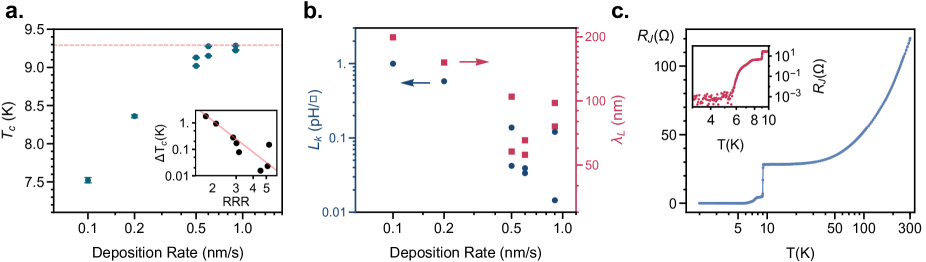
For electron beam evaporation (the deposition technique used here) vacuum pressures are reduced as low as possible during deposition, however are limited to the \qtye-8\milli¯ range by the hardware. With the contaminant flux fixed by the deposition system vacuum pressure, we explore the effect of deposition rate on Nb purity. By measuring the resistivity of a film with a known geometry at varying temperatures, we obtain a wealth of information about the film properties. In Fig. A1a we plot the superconducting transition temperature (proportional to the superconducting gap ) as a function of metal deposition rate. We observe that higher rates yield increased transition temperatures, which approach those found in bulk high-purity Nb [55], indicating that the films are increasingly pure. Indeed, we can also correlate the residual resistivity ratio , an indicator of superconductor quality, with deviations of measured critical temperature the bulk value , supporting the notion that higher deposition rates yield higher-quality films. Due to the extreme local temperatures required, practical considerations and stability concerns put a limit on feasible deposition rates. Nonetheless, despite variations induced by vacuum conditions, we find that rates above \qty0.6/ are required to deposit a film with high purity.
We can go further to examine the degree of disorder in the superconductor by probing the kinetic sheet inductance where is extracted from the film thickness , and the resistivity just above the superconducting transition. The sheet inductance also yields the London magnetic penetration depth . In Fig. A1b we find that both and are also reduced with films deposited at higher rates. Lower kinetic inductance and shorter London lengths indicate a lower degree of disorder in the superconductor, suggesting that increased deposition rates bring the material further away from the disordered dirty superconductor limit () [56].
We verify the superconducting contact quality between the wiring layer and the counter-electrode, as well as the junction tunnel barrier transparency by measuring the voltage accross a chain of 12 junctions in series, through which we send a fixed excitation current of \qty10. In Fig. A1c we plot the per-junction specific resistance as a function of temperature, showing the immediately apparent superconducting transition above \qty9. Immediately below the transition, the superconducting gap is still relatively low, and the junction critical currents fall below the excitation current, so a small resistance is observed. However as we decrease the temperature, we find that the resistance shrinks by several orders of magnitude (below the noise floor of the instrument). This indicates that the sum of any remaining resistance channels in a single junction is likely well below the m range, suggesting a superconducting contact between the Nb wiring layer and the Nb counter-electrode.
Appendix C Lossy Plasma Etch Residues
By virtue of size, the electric field concentration in a junction is orders of magnitude higher than in the qubit capacitor (or any planar structure such as the resonator capacitor), meaning the participation ratio [53] of the junction side surfaces will also be much higher. As such, our junction loss is likely still limited by the presence of lossy dielectrics formed on the sides of the junction, which for our design are primarily either spacer material, metal oxides, or residues left by the reactive ion etching process. As we cannot use more aggressive spacer [36] or oxide removal methods [18] without further risking the integrity of the aluminum junction barrier, we instead study the etch residues and discuss mitigation strategies.
Alongside the desired chemical and mechanical processes that remove niobium, reactive ion etching hosts a variety of simultaneous mechanisms that can grow material: etched material can either be re-deposited by sputtering, low-energy reaction products can re-adsorb onto exposed surfaces, and components in the plasma can react with exposed material [34]. The products of all of these mechanisms tend to be much more difficult to remove, so end up staying behind after the photoresist is dissolved, particularly on vertical walls not directly exposed to plasma bombardment during the etch. While the deposited material passivates the walls of the etched region during the etch and can produce high-aspect ratio features, for our junctions its critical to reduce any excess dielectrics, so we explore ways to understand and mitigate these residues in order to reduce loss.
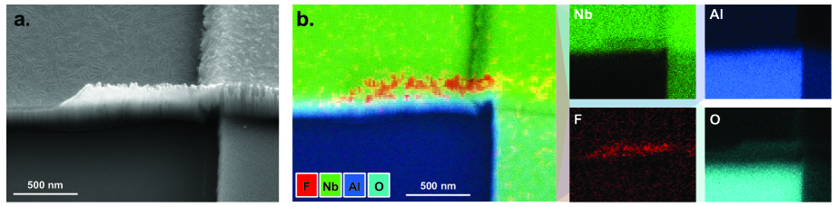
In Fig. A2a we show an example of a dielectric residue located on the side of a junction, which has not been removed throughout the entire fabrication process. This material must be formed during the third dry etch (Fig. 1f) since it covers and extends off the sides of the Nb wiring and counterelectrode layers. The residues appear to be present on all vertical surfaces exposed by the etch, visible as striations on the junction sides. To determine the deposition mechanism for this residue, we probe the chemical composition of the residue using energy dispersive spectroscopy (EDS). A composite map of normalized element composition is overlaid on the same image of the residue in Fig. A2b, with individual normalized element concentration maps shown to the right. As expected, we observe high Nb concentrations in the metal regions, and high aluminum and oxygen concentrations in the sapphire region, but more importantly we observe a significant concentration of fluorine in the residue (carbon is also observed in this region as well, but cannot be quantified due to high background carbon levels). This heavily suggests the residue is some kind of fluorocarbon polymer.
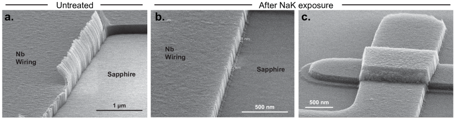
Fluorocarbons are chemically inert and robust against most standard solvents, acids, or oxygen plasma, and the residues remain largely unaffected by these conditions. However, fluorocarbon polymers are susceptible to defluorination by strong alkali reductants such as sodium-potassium amalgam (NaK) [57, 58]. In Fig. A3a we show a device with particularly extensive residues covering and extending off the sides of the wiring layer. In an oxygen-free dry nitrogen glovebox, we immerse the sample surface in a sodium-potassium amalgam (NaK) for \qty15min, rinse with tetrahydrofuran, move the sample into air, finish rinsing with acetone and isopropanol, then image the residues. In Fig. A3b-c we observe that the residue material is largely removed: the overhanging features have been removed, as well as the material on metal sides, with the original extent of the residue (about \qty30) apparent by the indentation left on the sapphire by the residue during the etch. This corroborates the hypothesis that these residues are composed of fluorocarbons, since the material could be removed upon treatment with NaK, wherein the amalgam cleaves the problematic C-F bonds and allows the remaining residues to become soluble in organic solvents.
While this NaK treatment appears promising on the microscopic scale, in practice the amalagam is difficult to keep clean, and leaves behind significant quantities of dust and salt deposits on the chip surface. A more practical method to post-clean any residues left behind by the etch might be to instead use a solution with a high reducing potential such as sodium napthalenide [57], commonly used as a surface treatment for PTFE. Regardless, the best way to remove the residues is to not form them in the first place, which is achieved by optimizing the etch plasma conditions. First, we remove obvious residue sources by ensuring the plasma chamber is thoroughly cleaned with oxygen, and no fluorinated vacuum oils are present in the system. We find that using gas constituents with low hydrogen and carbon content (eg. \ceSF6 or \ceCF4) significantly reduces the residue growth: in particular we find \ceCHF3 and \ceC4F8 readily polymerize. However, we note that using too much \ceSF6 can lead to the incorporation of sulfur [59] into any exposed \ceSiO2, which forms an even more inert residue and should be avoided. The addition of \ceO2 in the plasma can also help increase the carbon-fluorine ratio of the plasma [60], but also increases resist etch rate and passivates exposed metal. Using a low density plasma with a long mean free path for the radicals is key to increasing the etch rate and reducing re-deposition, as it increases the effective reactant and product temperature. Residue formation is also particularly sensitive to substrate temperature. With the substrate too cold, the reaction product temperature becomes low enough to allow recondensing, leading to increased fluorocarbon deposition. If the substrate is too hot, reactivity of the photoresist polymers is increased, promoting crosslinking, polymerization, and fluorination: thus good thermal contact between the substrate and the carrier wafer is essential, as the high temperature plasma can otherwise significantly heat the substrate. Finally, we observe the residue formation accelerates when the insulating substrate is exposed (likely a result of screening charges focusing the plasma towards remaining metal), so we ensure the etch is stopped within \qty15 of completion.
Appendix D Junction Area Dependence
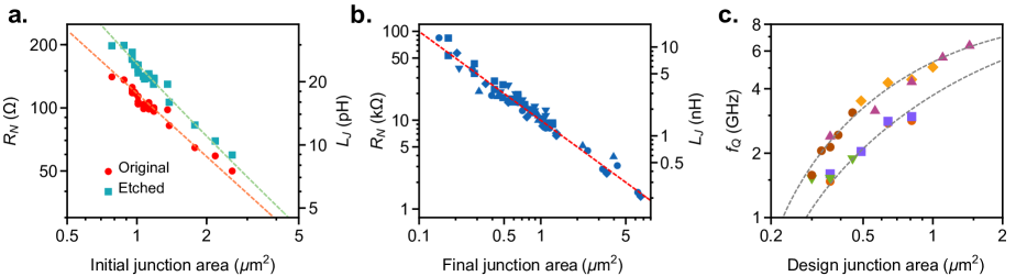
Having verified the relationship between the normal state resistance , the critical current and the gap energy [41] (see Fig. 2), we can use room temperature resistance measurements to efficiently predict cryogenic juction properties. In Fig. A4a, we show room temperature junction resistance and junction inductance (calculated from resistance using the product), plotted as a function of junction area (corrected for lithographic reduction). The original un-treated (see Fig. 1f) junction resistances are in good agreement with the expected inverse dependence on junction area, enabling us to fit the original critical current density. After etching the spacer (see Fig. 1g) some of the aluminum is removed as well, and the resistance increases since the effective junction dimensions have shrunk. By fitting the etched junctions, we extract an dimension reduction of approximately \qty160, which corresponds to about \qty80 of aluminum that gets removed by the etch. We note that this sets a practical limit on how small the junction can be before etch effects become more significant than lithographic definition of junction area.
Fitting junction resistances as a function of the final junction area (taking into account the dimension reductions) yields the true critical current density for the final junctions (Fig. A4b). We repeat these measurements for wafers with different processing conditions to populate Fig. 2b. A spread (typically between 5-10%) is noticeable in our junction resistance for a given junction area. While higher than typical niobium trilayer junction non-uniformity [29, 30], our junction variance can primarily be attributed to relatively large geometric deviations due to the limits of our lithographic resolution, which is compounded by fluctuations in the etch dynamics that determine the final junction area. Because of this we cannot probe the uniformity of the trilayer barrier itself, however estimate that it behaves similarly as in other trilayer junctions investigated, implying that our junction parameter spread could likely be reduced with higher resolution lithography methods and a more selective spacer removal technique. We test the functional limits of our junction reproducibility by measuring deviations of qubit frequencies across different chips from different wafers. In Fig. A4c, we show qubit frequencies (determined by junction inductance) as a function of design qubit junction area for devices with two different qubit capacitor designs. After determining the qubit capacitance and applying the estimated junction area reductions, we find the measured frequencies are self-consistent within 10 percent or so, even across separate wafers.
Appendix E Junction Annealing Mechanism
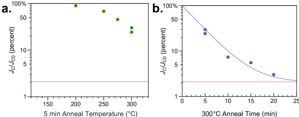
The effect of process temperature is readily apparent when comparing the resulting critical current densities of junctions with PECVD spacers (deposited at \qty300) and those with HDPCVD-grown spacers (\qty90). In Fig. 2b, for the high temperature PECVD junctions, we observed an approximately 2.3% reduction in . We investigate this effect in more detail by annealing finished low temperature (HDPCVD) junctions with initial in a dry \ceAr atmosphere, then re-measuring their critical current density.
In Fig A5a, we plot the annealed as a percentage of the untreated , and confirm that the annealing effect activates above \qty200, in agreement with [38]. In Fig. A5b we show the critical current density of junctions annealed at \qty300 for various lengths of time. After about \qty20min (the approximate time wafers spend at \qty300 during PECVD) we find that the current density reduction approaches the measured ratio between the PECVD and HDPCVD junctions. This suggests the high-temperature process dynamically anneals the junction barrier, likely increasing mobility and in the oxide barrier which enables diffusion and reduces pinhole density [46]. Qualitatively, this process appears to be exponential in time, so we overlay a saturating exponential fit of the form , where is the observed reduction factor, and obtain a critical time . The observed annealing effect is consistent with the critical current densities measured in Ref. [28] which do not exceed \qty190 during the fabrication process. With this in mind, our PECVD process could be modified to produce high critical current density junctions by either reducing the deposition temperature below \qty200 or to a lesser extent by limiting the time spent at elevated temperatures.
Appendix F Qubit Geometry and Experimental Setup
The qubit, readout resonator and other structures are formed in the same steps as the junction. We base our design on a qubit geometry [48] popular for it’s reduced radiation profile, a result of the cross-shaped coplanar qubit capacitor whose local electric dipole moments act to cancel each other out far away. In our case, the cross shape (typically used to implement qubit-qubit coupling or additional charge drives) isn’t strictly necessary and a coplanar capacitor composed of any two-dimensional shape would work as well. We also make an effort to minimize coupling to lossy two-level systems in surface dielectrics by rounding sharp corners where possible in the geometry. This reduces electric field concentration at specific points in the capacitor, leaving a weaker and more homogenous electric field which should couple less strongly to individual two-level systems.
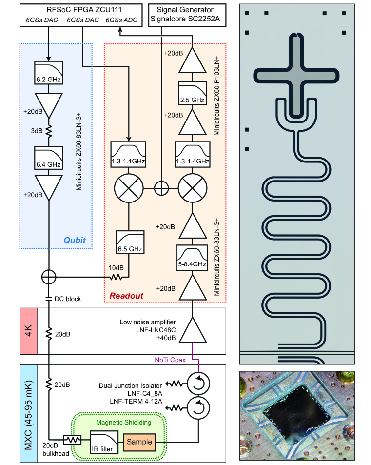
An example of our qubit geometry is shown in a composite microscope image on the top right of Fig. A6, imaged after Etch 3 (Fig. 1f). The niobium and un-etched aluminum have visibly different colors, allowing us to distinguish between the wiring layer and the base electrode. In our geometry, the qubit capacitor is formed with both layers, while the rest of the circuit and the majority of the chip (ground plane, readout resonator and coupling waveguides) is formed with just one layer. We find that the wiring layer readout resonators exhibit lower loss (See Appendix G), so typically pick the wiring layer for the ground plane. However having measured devices with both configurations (majority wiring layer and majority base electrode), we don’t find extreme differences in qubit properties, where the fields participate in both layers regardless of orientation. As an example, compare base-electrode ground plane wafer D with wiring ground plane wafer A in Fig. 3a, whose qubit quality factors are similar.
The qubits are capacitvely coupled to a meandered quarter wave coplanar waveguide resonator, which is in turn inductively coupled to a transmission line for readout. For simplicity, we couple directly to the readout resonator without additional purcell filtering. Chips containing up to 6 qubits and resonators are mounted in a copper circuit board shown in the bottom right of Fig A6, which is in turn bolted to a copper post thermalizing the assembly to the base temperature of an Oxford Triton 200 dilution refrigerator with minimum mixing chamber temperatures between \qtyrange[range-units = single,range-phrase = –]4595\milli. The mounted assembly is encased in two layers of Mu-metal magnetic shielding to reduce decoherence from stray magnetic fields, the qubits are isolated from microwave noise through an Eccosorb CR-110 high-frequency absorbing filter as 60 dB of cryogenic attenuation which keep the input noise close to the mixing chamber temperature. Transmitted microwave signals pass through two wideband circulators (isolating the qubits from microwave noise from the output side) into a low-loss superconducting NbTi coaxial cable, then are amplified by a low noise cryogenic amplifier followed by additional room temperature amplification.
Resonators and qubit transitions are characterized with single and two-tone spectroscopy using a Agilent E5071C network analyzer. For pulsed qubit measurements, we use a Quantum Instrument Control Kit [61] based on the Xilinx RFSoC ZCU111 FPGA. Qubit pulses are directly synthesized by the FPGA, while measurement pulses are generated with a heterodyne conversion setup, as shown in Fig. A6. With the spectral layout of each device determined, we select filter networks to minimize unwanted images and harmonics from the FPGA for both the qubit and readout pulses, with a broadband example configuration shown in Fig. A6. The FPGA and carrier signal generator are clocked to a 10 MHz rubidium source for frequency stability.
Appendix G Material Loss Probed by Resonator Quality Factor
To compare qubit loss contributions from material sources with contributions from the junction itself, we measure quality factors for readout resonators subject to the same fabrication conditions, but with no qubits attached. A typical normalized transmission spectrum of a resonator taken at a low average photon number () is shown in the inset of Fig. A7a. On resonance, we observe a dip in magnitude, which at low powers is described well by [62]:
| (1) |
where and the coupling quality factor has undergone a complex rotation due to minor impedance mismatches. We plot fitted internal quality factors in Fig. A7a, finding that increases with power. This behavior is entirely captured by a power dependent saturation mechanism [63], suggesting the dominant loss mechanism in the resonators arises from coupling to two-level systems.
We futher investigate limits on the resonator loss by using increased temperatures to further saturate the two-level systems. In Fig. A7b we plot measured at as a function of temperature (grouped by fabrication layer), with solid lines corresponding to a model of the form
| (2) |
where is the saturating loss mechanism from two-level systems [63], is a temperature independent upper bound arising from other sources of loss, and the conduction loss is given by [54]:
| (3) |
where and are the real and imaginary parts respectively of the complex surface impedance, calculated by numerically integrating the Mattis-Bardeen equations for and [54]. is constrained to the values measured in Appendix B, and is used as a fit parameter.
Comparing resonators formed during different steps in the fabrication process, we observe that resonators made from the wiring layer exhibit consistently higher quality factors, while resonators from the base layer are lossier and much more variable. Since the sides of the base layer have been exposed to more fabrication steps than the wiring layer, the surface niobium of this layer has a much longer chance to oxidize, and has the additional potential to host lossy dielectrics from un-removed spacer material. Thus, while we have improved losses in the wiring layer to about by reducing fluorocarbon formation, our devices are still loss-limited to approximately by two-level systems in the surfaces of the base electrode.
To investigate the relationship between qubit and readout resonator decoherence, we also measure quality factors of the readout resonator for each qubit. At single-photon powers, the readout resonator is maximally susceptible to material-based loss from two-level systems in its surface, but due to the hybridization of its electric field with the qubit mode will also interact with the materials in the qubit. In Fig. A7c we compare qubit quality factors with the single-photon readout quality factor for each of the devices from Fig. 3. On average, we observe that the two quality factors are close to a one to one relationship (as indicated by the grey line), with device variations within a factor of 3 or so. While a direct correlation between the two cannot be extracted from this data, this is to be expected for loss dominated by inhomogeneous material defect distributions between the resonator and qubit. Nevertheless, the similarity of the two quality factors leads us to conclude the qubit and resonator are likely limited by similar decoherence mechanisms.