Resonant Anti-Reflection Metasurface for Infrared Transmission Optics
Abstract
A fundamental capability for any transmissive optical component is anti-reflection, yet this capability is challenging to achieve in a cost-efficient manner over longer infrared wavelengths. We demonstrate that Mie resonant nanophotonic structures enhance transmission in Silicon, allowing it to function as an effective optical material over long-wave infrared wavelengths. This approach enables a window optic with up to 40% greater transmission than equal thickness unpatterned Si. Imaging comparisons with unpatterned silicon and off-the-shelf Germanium optics are shown, as well as basic broadband slant edge MTF measurements. Overall, we demonstrate how Mie-resonant structures can be used to improve optical transmission through window optics of arbitrary lithographically patternable optical media, and highlight their possible use in imaging applications.
keywords:
metasurface, mie resonance, transmission enhancementThe University of California, Los Angeles] Department of Materials Science and Engineering, University of California, Los Angeles, Los Angeles, CA 90024 The University of California, Los Angeles] Department of Materials Science and Engineering, University of California, Los Angeles, Los Angeles, CA 90024 The University of California, Los Angeles] Department of Materials Science and Engineering, University of California, Los Angeles, Los Angeles, CA 90024 \abbreviationsMTF,LWIR
1 Introduction
Increasing transmission efficiency of optical components is broadly desirable in optical system design across all wavelengths. Over long-wave infrared wavelengths, and for applications such as thermal imaging, high transmission efficiency is key for desirable performance due to the intensity-sensing nature of microbolometer array based detectors1, 2. Single or multi-layer thin film interference coatings are today’s standard for anti-reflection and transmission enhancement, and considerable study has been devoted to their development3, 4, 5. However, this approach requires a materials specific coating stack engineering, which can be difficult and time consuming depending on the system.6, 7, 8, 9, 10, 11 This is because coating materials with desirable refractive index and absorption over a given band may not exist, and must be mechanically compatible with other stack materials. These difficulties are compounded by the desire for stacks which achieve some combination of durability, angular acceptance, and polarization insensitivity. Over longer wavelengths the thicknesses of the layers and overall stack increase substantially, resulting in both added costs and limits to performance.
An alternative approach to anti-reflection is to use gradient index structures, which can be achieved in a variety of ways. To enable a gradual change in the refractive index along a depth dimension, gradient index structures are typically achieved using either depth modulated material aggregate/sol-gel based coatings or alternatively, by using so called ”moth-eye” anti-reflective structures. In the aggregate approach, nanoparticles are aggregated or created using processed chemical precursors, with sol-gels generally used to tailor particle densities at the interface in order to achieve a gradient index12, 13, 14, 15, 16. Other recent methods have used spinodal separation methods followed by etching to create porous structures17, 18. In contrast, moth-eye geometries take advantage of sub-wavelength porous or high aspect ratio cone and pillar geometries which are fabricated by directly etching the surface of a substrate, and which can be treated as effective media used to minimize index mismatch between air and the substrate interface19, 20, 21, 22, 23, 24, 25, 26. While these approaches can compete with and even exceed thin film coating based approaches in terms of raw transmissivity, there is evidence that in the case of random structures, diffuse scattering can be significant depending on their geometry27, 28 which would cause reduced contrast when imaging. Additionally, the geometries of these structures often result in increased mechanical fragility and susceptibility to environmental contamination and abrasion, which can greatly reduce their performance in outdoor or other harsh environments.29, 30, 31, 32
More recently, another approach to anti-reflection has emerged using resonant photonic structures at the interface between two media to more efficiently couple light into a substrate. Unlike gradient index-based approaches, resonant anti-reflection approaches use sub-wavelength photonic structures that are durable, robust, and more easily fabricable. Early work investigated using metallic surface resonator elements which leveraged a dipole resonance to achieve anti-reflection and preferentially forward scatter light33, 34, 35. Later work introduced an alternative method, employing all dielectric Mie-resonant structures36, 37, 38, 39, 40 as opposed to plasmonic resonators. This approach had the advantage of only requiring a high index dielectric substrate material and has primarily been explored over visible and UV wavelengths for absorption enhancement in solar cells41. All dielectric anti-reflection is enabled as a result of destructive interference between excited electric and magnetic dipole moments within the structure 42, also referred to as the substrate-mediated Kerker effect43. Theoretical conditions to maximize the effectiveness of this resonance-based approach have also been established44. Further developments enhanced the bandwidth of anti-reflection using multi-resonant surfaces45, as well as the previously-discovered effective index support46 of Fabry-Perot resonances47. While actively explored for solar absorption enhancement, to our knowledge, resonant anti-reflective approaches have not been demonstrated for transmission optics. A key challenge is that for transmission, as opposed to absorption, anti-reflection must enable preservation of the incident wavefront through the optical element and back out to free space. Such a capability is of particular interest to long-wave infrared optical components, where anti-reflection via either a conventional thin film or gradient index approach is more challenging because of the thicknesses involved.
Motivated by this opportunity, here we propose and experimentally demonstrate a resonant-anti reflection approach to maximize transmission through an optical component while maintaining overall image quality. We optimize and engineer Mie-resonant nanophotonic structures, demonstrating first through simulations that the overall phase front of incident light is preserved, enabling the key capability required for use as a transmission component. We then fabricate the nanophotonic structures at the wafer-scale on both sides of a DSP Si wafer, demonstrating strong anti-reflection and transmission over the LWIR wavelength band, with up to 40% transmission enhancement through the wafer relative to bare Si. We furthermore measure and calculate a modulation transfer function (MTF) of the Mie-resonant-structure coated Si wafer and demonstrate image quality preservation, enabling utilization of these approach even for high-resolution imaging applications. Remarkably, our approach delivers capabilities with Silicon on par with best in class AR-coated Germanium windows, enabling the potential for low-cost window optics for infrared and thermal imaging applications.
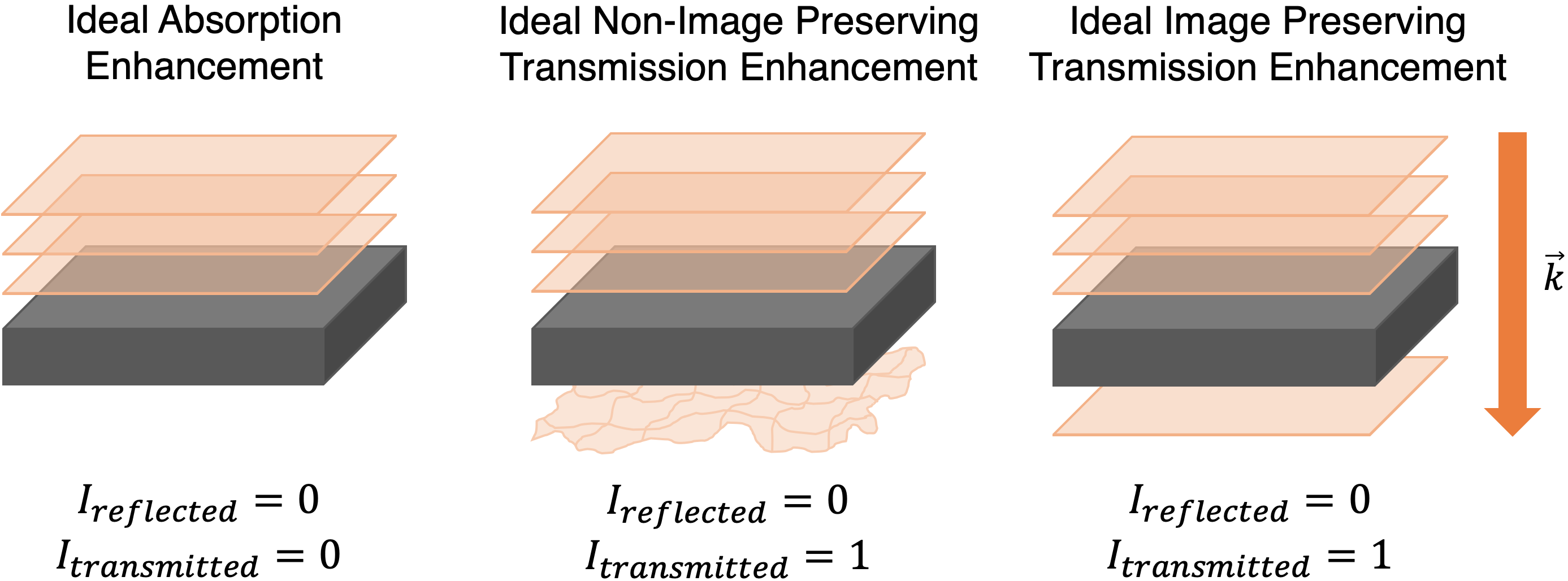
Mie-resonant anti-reflection has been actively explored for absorption enhancement, but there are important considerations that differentiate that application from imaging transmission enhancement. Broadly, we group the goals of anti-reflection and surface impedance matching into three main types, depicted in Fig. 1. The first type is absorption enhancement, motivated by applications such as solar cells. Here, the back plane of the solar cell is typically assumed to be a diffuse and fully reflective surface, and transmission through this surface is not considered. Light is intended to be coupled into the media and absorbed as efficiently as possible to generate greater photocurrent. The case in which back plane transmission is desirable (such as multi junction cells), but only maximization of optical power of a given band with no regards to image preservation, constitutes the second type. The final type occurs when power is maximized while also ensuring image preservation. The concept of ”image preservation” is meant to convey that the the wavefront integrity is preserved and not degraded to a degree which makes resolving an object impossible. Our investigation focuses on the image preserving case, which has not been explored in the LWIR range using a resonant based approach to our knowledge.
Dielectric Mie resonators can allow for excellent anti-reflection through the unique forward scattering phenomena enabled by an ensemble response of individual resonators. In our case, a subwavelength periodic array of resonators causes enhanced transmission through the interfaces of silicon at the LWIR wavelengths which maintains the integrity of the overall input wavefront. This approach is in principle highly broadband, omni-directional, and has minimal polarization sensitivity, all of which are desirable properties for an imaging optic. Additionally, the approach is entirely binary, enabling fabrication by conventional photolithographic means. We note that going against conventional Fresnel-law-based intuition, the all dielectric Mie-resonant approach relies on a large index contrast in order to produce high quality suppression of reflections. Optical materials generally used for transmission optics in the LWIR wavelengths such as Germanium and as we will demonstrate, Silicon, have suitably high refractive indices. This presents a unique opportunity to use the resonant approach to enable higher transmission efficiency in these wavelengths despite the large index contrast which would generally result in poorer reflective performance.
To investigate the effectiveness of this approach we opted to use Silicon as our material system, due to its wide availability, fabrication maturity, and its low overall transmission in the LWIR48, 49 ( 50% through a 500 thick bare substrate over the full band) which allows for significant and easily noticeable performance improvement. To demonstrate our approach, we chose to apply it to arguably the simplest optical component, a basic window. Window optics provide a clear and useful proof of concept platform for our approach. They are broadly employed in optical systems to prevent contact of more sensitive components with the environment, and act to prevent ingress of dust and humidity to the rest of a lens column. In short, they are ubiquitous and often necessary in optical systems.
Silicon’s relatively high intrinsic absorptivity in the LWIR means that it has not typically been used for imaging or window optics in the face of higher performance Ge, ZnSe, or ZnS alternatives. We note however that in the case of windows, large thicknesses may not be essential in fulfilling their protective functionality (i.e. when impact resistance or high pressure tolarance is not a necessary function of the window). In cases where imaging is desirable, more recent advances in metasurface design demonstrate that thin and flat focusing optical systems are possible, limiting the effects of silicon’s intrinsic absorptivity on optical performance.
We first numerically investigated and optimized resonant anti-reflective designs scaled for Silicon’s index and the LWIR wavelength range, evaluating a range of different lattice and feature geometries assuming 2 identically patterned interfaces. We simulated the designs using rigorous coupled-wave analysis (RCWA) while assuming fabricable critical feature sizes based on available tooling. To facilitate the optimization we developed a custom figure of merit shown as eq. (1) which rewarded integrated spectral transmittance through the optic while inflicting a severe penalty on unfabricable designs:
| (1) |
The result of this optimization, shown schematically in Fig. 2a, yielded the best performance of the designs explored within typical wafer-scale fabrication limits. We note here that the added integral term sought to reward higher transmission at more energetic wavelengths, but in principal, resonator size could be tailored to move the peak to longer wavelengths as well. E-field component plots for a demonstrative 16 m thick Si substrate are shown in Fig. 2b, which show the aspect of our design that is of particular importance to our application: the coherent character of the forward scattered waves through the interface, resulting from the overlap of electric and magnetic dipole resonance overlaps present. This phenomena occurs both when the waves are scattered into and out of the patterned high index media. Simulated spectral transmission comparisons are shown in Fig. 2c, highlighting the transmission performance increase we expect from our approach.
We highlight a portion of the optimization landscape in Fig. 2d, which shows a slice of the 3D optimization (Feature height, period, and feature width) at a feature height of . The y axis shows the trench width between each resonant element (the critical feature in terms of fabrication) while the x axis shows the multiplier of the trench width to determine the period. The period for a tile is then given by multiplying the x and y axis values for that tile. Our approach scans a large number of features while ensuring feature conflicts do not occur, such as a period which is lower in magnitude than a feature, which could yield unphysical simulation results.
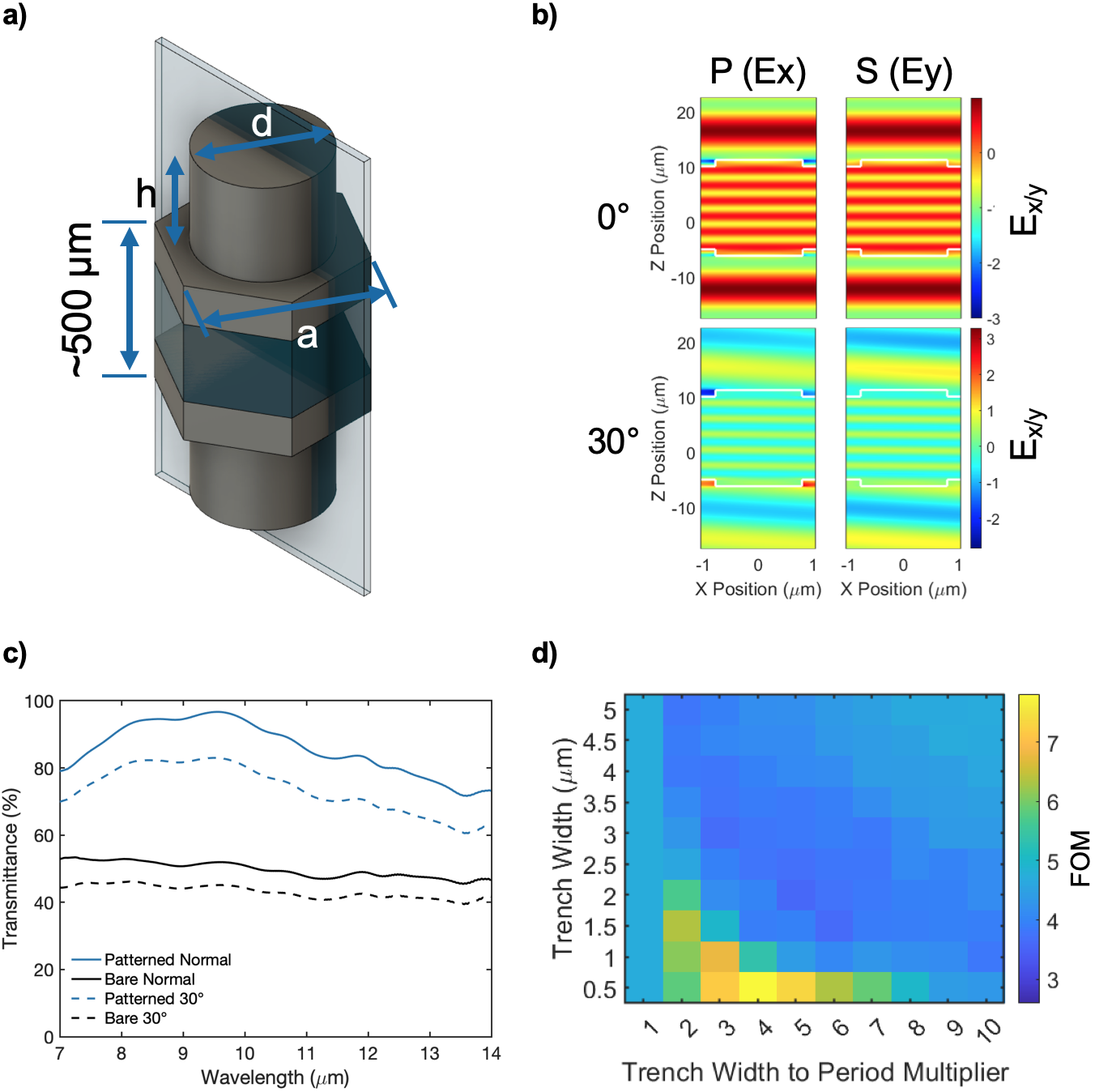
We fabricaated the optimal design on float zone process grown 500 thick double side polished intrinsic Si substrates. We lithographically patterned the optimized Mie-resonant photonic structures of hexagonally packed cylindrical pillars with a periodicity of , a height of , and a diameter of onto both sides of double side polished (DSP) Si wafers (see Materials and Methods). A high magnification SEM image of the design tilted at is shown in Fig. 3a showing good consistency and overall design fidelity.
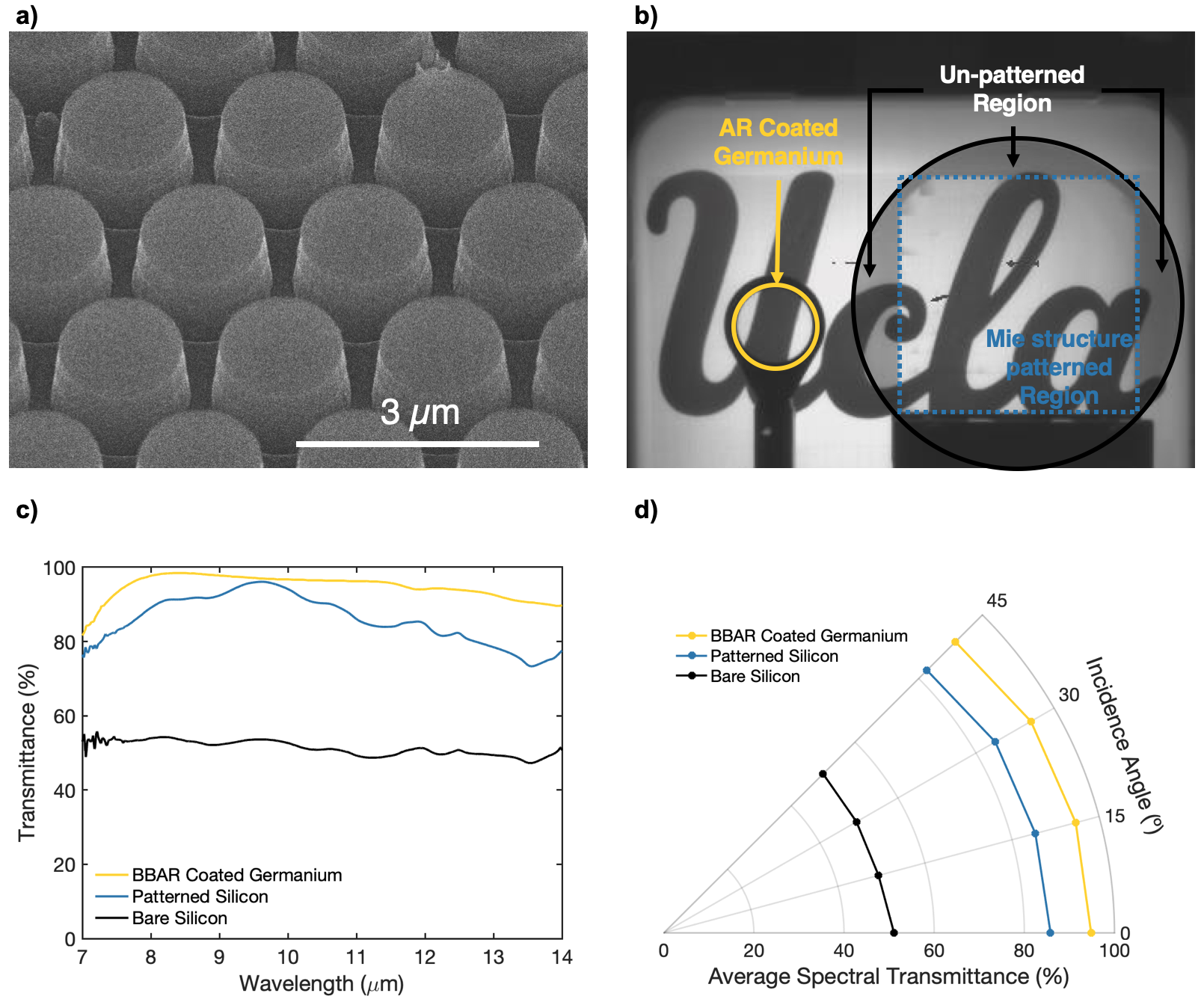
LWIR spectral measurements of the device can be seen in Fig. 3b, comparing the performance of a bare intrinsic Si wafer, a patterned intrinsic Si window, and a Ge optic. As the design is highly periodic, diffraction is a possible concern in terms of imaging, but we note that the patterned features are small enough with respect to the 7-14 band that they fall outside the diffractive regime for all incidence angles ( for the entire band). This lack of diffractive behavior can be observed in the E-field component plots in each polarization for 2 cross sectional cuts of the unit cell in Fig. 2b, showing no diffractive behavior in the propagation of the waves in either polarization or at angular incidence. Finally, as the window optic will be used in an imaging system, its transmission spectra is only a proxy for its true performance. In reality, if the surface relief structure causes undesirable scattering based effects, these will only manifest when imaging through the device. As an initial test, an image of a thermal target was taken through the patterned device, as shown in Fig. 3c. The square patterned area has a dotted outline, with wafer segments outside of this being unpatterned. A Ge LWIR AR coated window is also shown as a comparison, with areas outside both window regions acting as a control. A clear difference in transmission can be seen between these areas while imaging integrity is maintained.
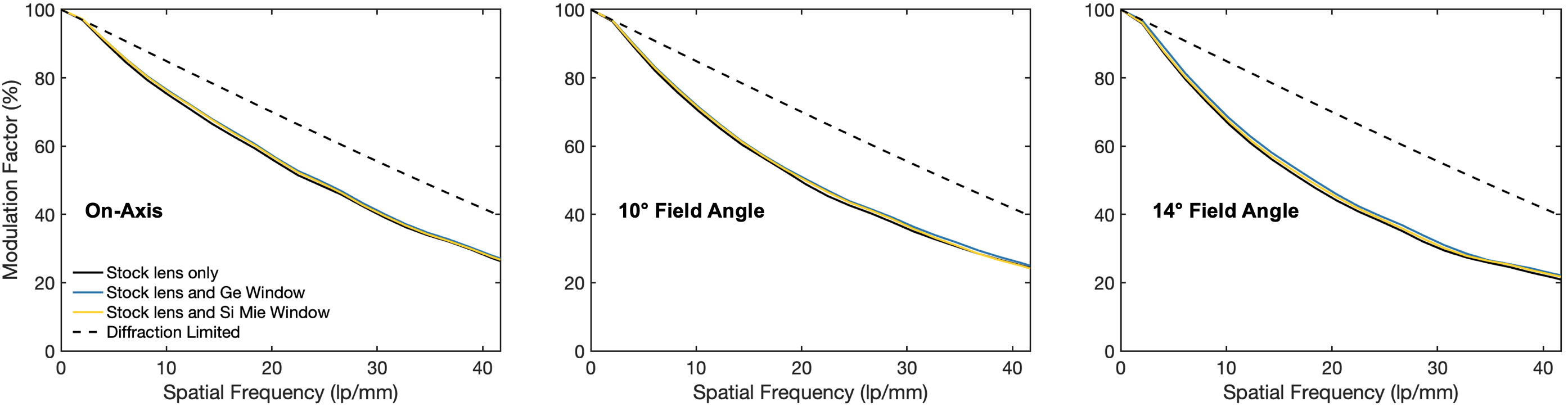
As a final and more quantitative demonstration of imaging performance, we performed a tangential broadband modulation transfer function (MTF) measurement using a slanted edge target through our patterned Silicon optic, an AR coated Germanium window, and with no window. Images were then taken at (on-axis), ( 70% field), and (Full-field) field angles. While the full field of view is around , enough of each side of the slant target needed to be visible in the image for proper measurement. Analysis and MTF calculation was done using sfrmat5, a publically available code used for MTF measurement of systems using slant edge targets.50 Comparisons at each field angle are shown in Fig. 4, showing that the MTF is comparable between our photonic Si optic, the commercial Ge optic, and the case without a window at all 3 field angles. We note that while this measurement was performed in as controlled a manner as possible with available equipment, it is primarily meant to demonstrate the comparison of our optic to notable alternatives, and not to serve as rigorously accurate MTF data. Additionally, while the response for each case is close, careful observation shows that the MTF with window optics added is higher than without, which we attribute to the frequency filtering of the window preferentially rejecting poorly corrected source wavelengths from entering the rest of the imaging system. The maximum effect with the added window over all plotted frequency points and angles only amounts to a difference of 3.6% in modulation factor.
In conclusion, we have demonstrated method based on resonant forward scattering microstructures to increase transmission in Si optical components over LWIR wavelengths. We show a performance increase of up to 40% with comparable performance to Ge at shorter wavelengths, where optical power incident on the detector is greatest. An intriguing future possibility exists in combining this high transmission patterning approach with focusing metasurface patterns on the opposing side of the same substrate to allow the use of Si LWIR optics, making it a viable alternative material platform in systems where throughput requirements are not as stringent. Additionally, the use of the Si in this configuration gives intriguing possibilities for its use in active opto-electronic systems over long-wave infrared wavelengths.
2 Supporting Information
Contains additional information on experimental setup and detailed fabrication methods.
This material is based upon work supported by the National Science Foundation (NSF CAREER) under Grant No. 2146577, the DARPA Young Faculty Award (W911NF2110345), and the Sloan Research Fellowship (Alfred P. Sloan Foundation). J.B. was supported by a National Science Foundation Graduate Research Fellowship under grants DGE-1650605 and DGE-2034835, as well as the NSF funded UCLA NRT-INFEWS Program under grant number (INFEWS)-DGE-1735325. Additionally, this work used computational and storage services associated with the Hoffman2 Shared Cluster provided by UCLA Office of Advanced Research Computing’s Research Technology Group. Fabrication of the devices shown in this work was done in the UCLA Nanolab Nanoelectronics Research Facility.
References
- Rogalski 2010 Rogalski, A. Infrared detectors; CRC press, 2010; pp 104–137
- Yadav et al. 2022 Yadav, P. V.; Yadav, I.; Ajitha, B.; Rajasekar, A.; Gupta, S.; Ashok Kumar Reddy, Y. Advancements of uncooled infrared microbolometer materials: A review. Sensors and Actuators A: Physical 2022, 342, 113611
- Dobrowolski 2010 Dobrowolski, J. A. In Handbook of Optics: Volume IV - Optical Properties of Materials, Nonlinear Optics, Quantum Optics, 3rd ed.; Bass, M., Ed.; McGraw-Hill Education: New York, 2010
- Musset and Thelen 1970 Musset, A.; Thelen, A. In IV Multilayer Antireflection Coatings; Wolf, E., Ed.; Progress in Optics; Elsevier, 1970; Vol. 8; pp 201–237
- Kaiser and Pulker 2013 Kaiser, N.; Pulker, H. K. Optical interference coatings; Springer, 2013; Vol. 88
- Raut et al. 2011 Raut, H. K.; Ganesh, V. A.; Nair, A. S.; Ramakrishna, S. Anti-reflective coatings: A critical, in-depth review. Energy and Environmental Science 2011, 4, 3779–3804
- Shanbhogue et al. 1997 Shanbhogue, H. G.; Nagendra, C. L.; Annapurna, M. N.; Kumar, S. A.; Thutupalli, G. K. M. Multilayer antireflection coatings for the visible and near-infrared regions. Applied Optics 1997, 36, 6339
- Wang et al. 2021 Wang, H.; Zheng, Z.; Ji, C.; Jay Guo, L. Automated multi-layer optical design via deep reinforcement learning. Machine Learning: Science and Technology 2021, 2, 025013
- Hedayati and Elbahri 2016 Hedayati, M. K.; Elbahri, M. Antireflective coatings: Conventional stacking layers and ultrathin plasmonic metasurfaces, a mini-review. Materials 2016, 9
- Hossain et al. 2019 Hossain, J.; Mondal, B. K.; Mostaque, S. K.; Ahmed, S. R. A.; Shirai, H. Optimization of multilayer anti-reflection coatings for efficient light management of PEDOT:PSS/c-Si heterojunction solar cells. Materials Research Express 2019, 7, 0–9
- Berning 1962 Berning, P. H. Use of Equivalent Films in the Design of Infrared Multilayer Antireflection Coatings. J. Opt. Soc. Am. 1962, 52, 431–436
- Bautista and Morales 2003 Bautista, M. C.; Morales, A. Silica antireflective films on glass produced by the sol–gel method. Solar Energy Materials and Solar Cells 2003, 80, 217–225
- Mizoshita et al. 2015 Mizoshita, N.; Ishii, M.; Kato, N.; Tanaka, H. Hierarchical Nanoporous Silica Films for Wear Resistant Antireflection Coatings. ACS Applied Materials & Interfaces 2015, 7, 19424–19430
- Zhang et al. 2014 Zhang, Y.; Zhao, C.; Wang, P.; Ye, L.; Luo, J.; Jiang, B. A convenient sol–gel approach to the preparation of nano-porous silica coatings with very low refractive indices. Chemical Communications 2014, 50, 13813–13816
- Mahadik et al. 2015 Mahadik, D. B.; Lakshmi, R. V.; Barshilia, H. C. High performance single layer nano-porous antireflection coatings on glass by sol–gel process for solar energy applications. Solar Energy Materials and Solar Cells 2015, 140, 61–68
- Wang et al. 2020 Wang, J.; Zhang, H.; Wang, L.; Yang, K.; Cang, L.; Liu, X.; Huang, W. Highly Stable and Efficient Mesoporous and Hollow Silica Antireflection Coatings for Perovskite Solar Cells. ACS Applied Energy Materials 2020, 3, 4484–4491
- Zhang 2022 Zhang, Z. Antireflective film of porous silica. Journal of the Optical Society of America A 2022, 39, 1172–1178
- Zhang 2022 Zhang, Z. Dust proof properties of spinodal porous surfaces. Journal of the Optical Society of America A 2022, 39, 866–872
- Huang et al. 2007 Huang, Y.-F.; Chattopadhyay, S.; Jen, Y.-J.; Peng, C.-Y.; Liu, T.-A.; Hsu, Y.-K.; Pan, C.-L.; Lo, H.-C.; Hsu, C.-H.; Chang, Y.-H.; Lee, C.-S.; Chen, K.-H.; Chen, L.-C. Improved broadband and quasi-omnidirectional anti-reflection properties with biomimetic silicon nanostructures. Nature Nanotechnology 2007, 2, 770
- Southwell 1983 Southwell, W. H. Gradient-index antireflection coatings. 1983, 8, 584–586
- Sun et al. 2008 Sun, C. H.; Jiang, P.; Jiang, B. Broadband moth-eye antireflection coatings on silicon. Applied Physics Letters 2008, 92, 2006–2009
- Yuan et al. 2009 Yuan, H.-C.; Yost, V. E.; Page, M. R.; Stradins, P.; Meier, D. L.; Branz, H. M. Efficient black silicon solar cell with a density-graded nanoporous surface: Optical properties, performance limitations, and design rules. Applied Physics Letters 2009, 95, 123501
- Branz et al. 2009 Branz, H. M.; Yost, V. E.; Ward, S.; Jones, K. M.; To, B.; Stradins, P. Nanostructured black silicon and the optical reflectance of graded-density surfaces. Applied Physics Letters 2009, 94, 231121
- Koynov et al. 2006 Koynov, S.; Brandt, M. S.; Stutzmann, M. Black nonreflecting silicon surfaces for solar cells. Applied Physics Letters 2006, 88, 203107
- Zhu et al. 2009 Zhu, J.; Yu, Z.; Burkhard, G. F.; Hsu, C.-M.; Connor, S. T.; Xu, Y.; Wang, Q.; McGehee, M.; Fan, S.; Cui, Y. Optical Absorption Enhancement in Amorphous Silicon Nanowire and Nanocone Arrays. Nano Letters 2009, 9, 279–282
- Zhu et al. 2010 Zhu, J.; Hsu, C.-M.; Yu, Z.; Fan, S.; Cui, Y. Nanodome Solar Cells with Efficient Light Management and Self-Cleaning. Nano Letters 2010, 10, 1979–1984
- Sánchez-Gil and Nieto-Vesperinas 1991 Sánchez-Gil, J. A.; Nieto-Vesperinas, M. Light scattering from random rough dielectric surfaces. Journal of the Optical Society of America A 1991, 8, 1270–1286
- Gonzalez et al. 2014 Gonzalez, F. L.; Morse, D. E.; Gordon, M. J. Importance of diffuse scattering phenomena in moth-eye arrays for broadband infrared applications. Optics Letters 2014, 39, 13
- Yoo et al. 2019 Yoo, Y. J.; Kim, Y. J.; Kim, S.-Y.; Lee, J. H.; Kim, K.; Ko, J. H.; Lee, J. W.; Lee, B. H.; Song, Y. M. Mechanically robust antireflective moth-eye structures with a tailored coating of dielectric materials. Optical Materials Express 2019, 9, 4178
- García et al. 2011 García, M.; Marroyo, L.; Lorenzo, E.; Pérez, M. Soiling and other optical losses in solar-tracking PV plants in navarra. Progress in Photovoltaics: Research and Applications 2011, 19, 211–217
- Sarkı n et al. 2020 Sarkı n, A. S.; Ekren, N.; Sağlam, c. A review of anti-reflection and self-cleaning coatings on photovoltaic panels. Solar Energy 2020, 199, 63–73
- Lu et al. 2020 Lu, H.; Cai, R.; Zhang, L.-Z.; Lu, L.; Zhang, L. Experimental investigation on deposition reduction of different types of dust on solar PV cells by self-cleaning coatings. Solar Energy 2020, 206, 365–373
- Catchpole and Polman 2008 Catchpole, K. R.; Polman, A. Design principles for particle plasmon enhanced solar cells. Applied Physics Letters 2008, 93
- Atwater and Polman 2010 Atwater, H. A.; Polman, A. Plasmonics for improved photovoltaic devices. Nature Materials 2010, 9, 205–213
- Spinelli et al. 2011 Spinelli, P.; Hebbink, M.; De Waele, R.; Black, L.; Lenzmann, F.; Polman, A. Optical impedance matching using coupled plasmonic nanoparticle arrays. Nano Letters 2011, 11, 1760–1765
- Brongersma et al. 2014 Brongersma, M. L.; Cui, Y.; Fan, S. Light management for photovoltaics using high-index nanostructures. Nature Materials 2014, 13, 451–460
- Jahani and Jacob 2016 Jahani, S.; Jacob, Z. All-dielectric metamaterials. Nature Nanotechnology 2016, 11, 23–36
- Kivshar and Miroshnichenko 2017 Kivshar, Y.; Miroshnichenko, A. Meta-Optics with Mie Resonances. Opt. Photon. News 2017, 28, 24–31
- Kuznetsov et al. 2016 Kuznetsov, A. I.; Miroshnichenko, A. E.; Brongersma, M. L.; Kivshar, Y. S.; Luk’yanchuk, B. Optically resonant dielectric nanostructures. Science 2016, 354
- Pala et al. 2016 Pala, R. A.; Butun, S.; Aydin, K.; Atwater, H. A. Omnidirectional and broadband absorption enhancement from trapezoidal Mie resonators in semiconductor metasurfaces. Scientific Reports 2016, 6, 1–7
- Spinelli et al. 2012 Spinelli, P.; Verschuuren, M. A.; Polman, A. Broadband omnidirectional antireflection coating based on subwavelength surface Mie resonators. Nature Communications 2012, 3, 692–695
- van de Groep and Polman 2013 van de Groep, J.; Polman, A. Designing dielectric resonators on substrates: Combining magnetic and electric resonances. Optics Express 2013, 21, 26285
- Baryshnikova et al. 2016 Baryshnikova, K. V.; Petrov, M. I.; Babicheva, V. E.; Belov, P. A. Plasmonic and silicon spherical nanoparticle antireflective coatings. Scientific Reports 2016, 6, 1–11
- Wang et al. 2014 Wang, K. X.; Yu, Z.; Sandhu, S.; Liu, V.; Fan, S. Condition for perfect antireflection by optical resonance at material interface. Optica 2014, 1, 388
- Pecora et al. 2018 Pecora, E. F.; Cordaro, A.; Kik, P. G.; Brongersma, M. L. Broadband Antireflection Coatings Employing Multiresonant Dielectric Metasurfaces. ACS Photonics 2018, 5, 4456–4462
- Motamedi et al. 1992 Motamedi, M. E.; Southwell, W. H.; Gunning, W. J. Antireflection surfaces in silicon using binary optics technology. Applied Optics 1992, 31, 4371–4376
- Cordaro et al. 2019 Cordaro, A.; Van De Groep, J.; Raza, S.; Pecora, E. F.; Priolo, F.; Brongersma, M. L. Antireflection High-Index Metasurfaces Combining Mie and Fabry-Pérot Resonances. ACS Photonics 2019, 6, 453–459
- Chandler-Horowitz and Amirtharaj 2005 Chandler-Horowitz, D.; Amirtharaj, P. M. High-accuracy, midinfrared () refractive index values of silicon. Journal of Applied Physics 2005, 97
- Palik 1998 Palik, E. D. Handbook of optical constants of solids; Academic press, 1998; Vol. 3
- Burns and Williams 2018 Burns, P. D.; Williams, D. Camera resolution and distortion: Advanced edge fitting. IS and T International Symposium on Electronic Imaging Science and Technology 2018, 1–5