Design and optimization of a 100 keV DC/RF ultracold electron source
Abstract
An ultracold electron source based on near-threshold photoionization of a laser-cooled and trapped atomic gas is presented in this work. Initial DC acceleration to 10 keV and subsequent acceleration of the created bunches to 100 keV by RF fields makes the design suitable to serve as injector for accelerator-based light sources, single-shot ultrafast protein crystallography, applications in dielectric laser acceleration schemes, and potentially as an injector for free electron lasers operating in the quantum regime. This paper presents the design and properties of the developed DC/RF structure. It is shown that operation at a repetition frequency of 1 kHz is achievable and detailed particle tracking simulations are presented showing the possibility of achieving a brightness that can exceed conventional RF photosources.
keywords:
Ultracold electrons; Laser cooling; RF acceleration; Emittance; Beam brightness1 INTRODUCTION
In recent years an ultrafast and ultracold electron source (UCES) based on two-step, near-threshold photoionization of a laser-cooled and trapped atomic gas has been developed [1, 2, 3, 4, 5, 6, 7, 8]. The goal of a source of this type has been to offer a combination of a high beam quality and high bunch charge.
Sub-ps electron bunches with an energy of 10 keV and normalized transverse emittances in the order of a few nm rad have been measured [8]. Building upon this idea, a source is proposed that combines the benefits provided by the UCES with a radio frequency (RF) structure that increases the bunch energy to 100 keV whilst maintaining the excellent beam quality.
Applications for the proposed source are found in fields such as ultrafast electron diffraction (UED) where ultrafast dynamics of matter at the atomic scale can be studied through pump-probe experiments. A high quality electron bunch in terms of the transverse coherence length is required for such applications [9]. To realize this for a given beam size, an ultracold electron source is needed. The proposed source is capable of producing 10 fC bunches with a transverse normalized emittance in the order of nm rad such that even (single-shot) protein crystallography could be realized.
Furthermore, the design presented in this work may be considered as a suitable injector for an FEL operating in the quantum regime [10], or in the field of dielectric laser acceleration (DLA) where typically low-charge bunches are injected in microscopic structures, where very high transverse quality bunches are required [11].
The main selling point of the proposed source is based on the low transverse emittance of the electron bunches extracted from a laser-cooled atomic gas [8]. The bunches are however extracted at an energy of only 10 keV. Immediate acceleration after extraction should prove beneficial for bunch quality preservation as it reduces beam degradation due to Coulomb interactions.
For the structure presented in this work an emphasis is put on the design being simple, compact, and robust. Having only a few accelerating cells greatly simplifies both the manufacturing process and reduces the cost. Using a single waveguide to supply RF power (which will henceforth be referred to as the ’RF feed’) ensures phase stability and magnetic coupling through the wall connecting the two cells guarantees phase synchronization between the cells. Powering the structure and accelerating electrons from 10 keV to 100 keV requires only a 5 kW solid-state RF amplifier.
This paper presents the design, optimization, EM field simulations, and particle tracking simulations of a hybrid DC/RF structure [12], consisting of a grating magneto-optical trap (MOT) in a static extractor field [13, 14] and a 1-cell standing wave RF cavity. Source requirements and a general overview of the source are presented in Sec. (2), the source design and optimization strategy is presented in Sec. (3) along with electromagnetic field simulations and a thermal analysis. Finally, realistic particle tracking simulations are presented in Sec. (4).
2 SOURCE REQUIREMENTS AND OVERALL DESIGN
The electron source presented in this paper builds on an existing DC electron source, as well as other similar setups [1, 2, 3, 4, 5, 6, 7, 8] and a proposal for a hybrid DC/RF electron source [12]. The applications mentioned in Sec. (1) all require a high bunch quality and common for all applications is the requirement for a low transverse normalized emittance, which is given by the following:
| (1) |
where denotes the averaging of a parameter over the electrons in the bunch, the transverse position, , with the electron rest mass, the speed of light, the Lorentz factor, and the normalized electron bunch’s velocity in the -direction with respect to the speed of light.
The structure presented in this paper is designed to accelerate electron bunches to an energy of 100 keV, a commercially available solid-state RF amplifier (5 kW peak power) should provide the structure with sufficient power to accelerate the bunches to the desired energy, enabling repetition rates of kHz.
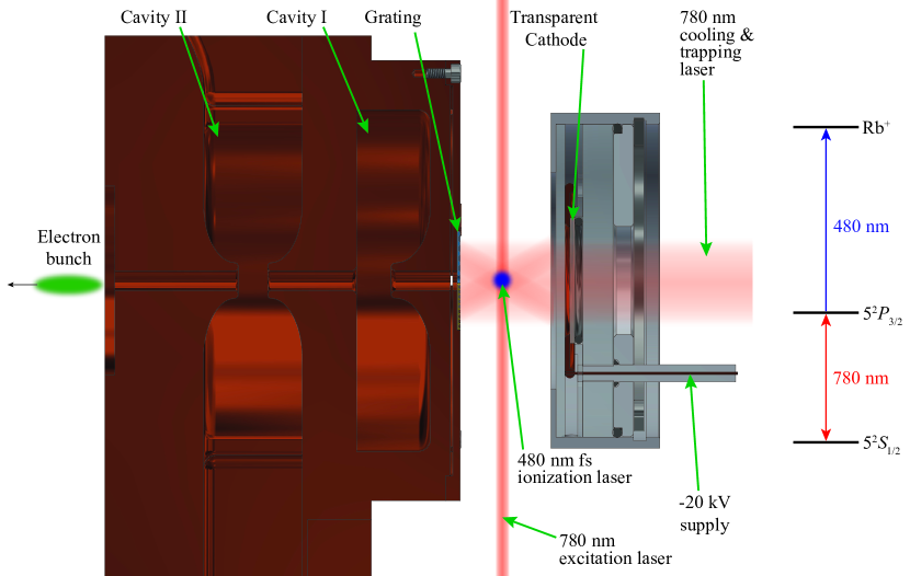
A schematic representation of the proposed source is shown in Fig. (1) with, from left to right: the copper RF structure housing the two cavities and a mounted grating chip, the region in which laser cooling and trapping occurs, and the accelerator module housing the -20 kV cathode. Electron bunches are created in the region between the cathode and the RF structure where the excitation and ionization lasers overlap.
A MOT is created by a single trapping laser beam, which passes through the ITO electrode (transparent cathode). This trapping laser at nm is diffracted on a grating chip consisting of three linear gratings oriented 120 degrees with respect to each other [8, 13]. The diffracted first orders create, together with the incident laser beam, a diamond-shaped region where laser-cooling of the 85Rb atomic gas can be realized (in combination with an anti-Helmholtz magnetic coil configuration (see Fig. (2)).
The atoms are ionized in a two-step process, shown in Fig. (1) on the right. They are first excited by the 780 nm excitation laser (red), which pumps the transition, and the femtosecond (fs) 480 nm ionization laser (blue) which ionizes the laser-cooled and trapped 85Rb gas, resulting in a ps duration electron bunch at an energy of 10 keV [15]. This bunch is then accelerated to 100 keV by the RF part of the source. The RF part is a 1-cell, magnetically coupled (not shown in this figure), standing wave, S-band (2.99855 GHz), -mode accelerator structure.
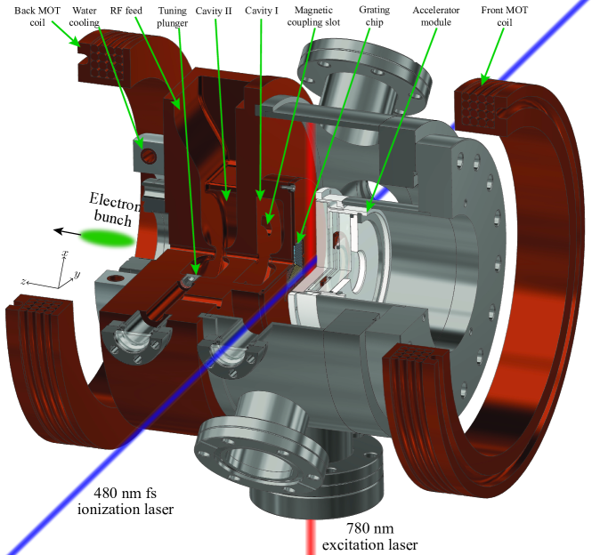
The two cells in the RF structure are magnetically coupled. Coupling through the cavity walls is necessary to minimize the required amount of RF power. Nose-cones in the cells ensure a sufficiently large shunt impedance. Power is fed into the second cell through a coupling slot with a modified WR284 waveguide. An auxiliary waveguide with a similar coupling structure located underneath the feed waveguide significantly reduces any induced dipole fields and also functions as a port for a vacuum pump. A tuning plunger is located in the second acceleration cell, which allows for tuning of the resonant frequency of the structure by 2 MHz. An impression of the source, complete with MOT coils, viewports for the lasers, and water cooling is shown in Fig. (2).
3 ACCELERATOR STRUCTURE
This section will discuss the accelerating structure used in the proposed source and describe the design and optimization of the newly designed RF structure. First, the DC-based UCES is briefly introduced and its merits discussed in section (3.1), followed by the newly designed RF structure, where the geometry, power feed, electromagnetic field distribution, and thermal properties of the source are presented in section (3.2 - 3.5) respectively.
3.1 DC structure
As mentioned earlier, the DC part of the proposed hybrid DC & RF electron source is based on a readily existing source [8]. This source produces electron bunches with a temporal length in the order of picoseconds at electron temperatures of 10 K [14, 15]. It does so through a two-step photoionization process with a broadband fs laser pulse ( nm FWHM). Being able to scan the central wavelength of this broadband spectrum enables the production of low excess energy electrons. The laser cooling takes place in a grating based magneto optical trap [13]. These bunches are created in the center of a static field with a potential of -20 kV applied across a distance of 19.2 mm, resulting in an accelerating gradient of 1.4 MV/m [8].
Creating electrons at higher energies is possible by increasing this acceleration voltage. There is however a practical limit for this due to dissimilar Stark shifts of the hyperfine levels of the excited state, which can be avoided by keeping the acceleration potential at MV/m [16, 17]. Therefore the applied potential is limited to -20 kV and additional acceleration is realized through an RF accelerator. The attainable repetition frequency of this source is not limited by the heating of a photo cathode but by the fs laser repetition frequency and the filling time of the MOT from which the electron bunches are extracted, allowing operation at kHz
3.2 RF structure
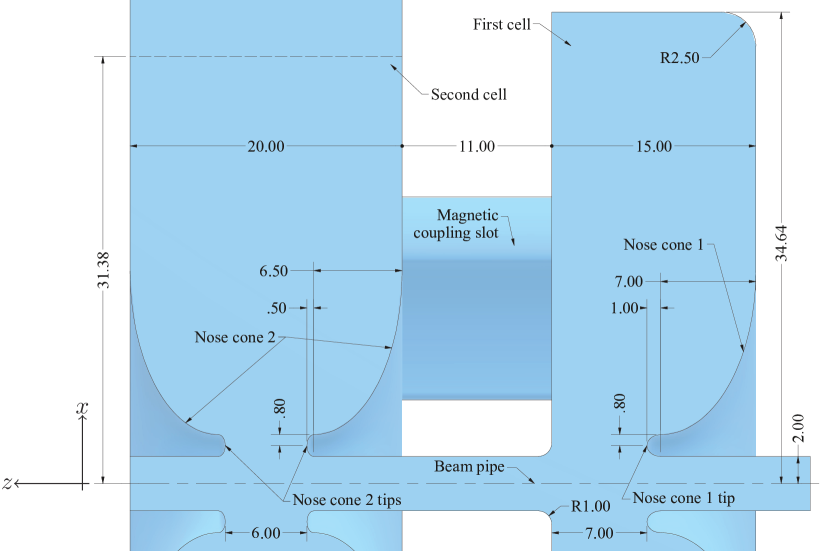
A schematic representation of the RF structure’s geometry in the plane is shown in Fig. (3). A multi-cell structure will always have a number of resonant frequencies equal to the amount of cells. These resonance frequencies will be visible in its absorption spectrum and are shown in Fig. (4), obtained from the frequency domain solver of cst microwave studio [18].
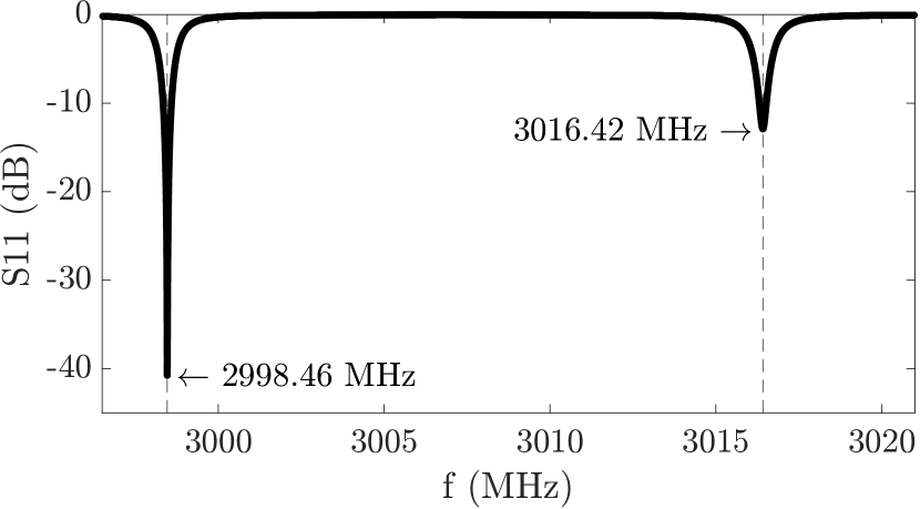
The absorption peak at MHz is the desired -mode of the structure with an input reflection of approximately -40.8 dB. The undesired zero-mode is found at MHz, giving a mode separation of roughly 18 MHz.
The structure shown in Fig. (3) is initially optimized by varying the major axes of the nose cones in order to minimize the power dissipation in the copper, increasing the quality factor of the structure. The width of the cell acceleration gaps (distance between the nosecone and cavity wall for the first cell and the distance between both nose cones for the second cell) is fixed at 7 mm and 6 mm, respectively.
The power dissipation is minimized by varying the minor and major axes of the elliptical nose cone tips. The nose cone structures in both cells are necessary because of the low velocity of the electron bunches (the electrons enter the RF field with ). The nose cones reduce the length along which the electrons are accelerated, ensuring a sufficiently short transit-time. Additionally, the nose cones increase the shunt impedance, utilizing the available power more efficiently.
The nose cones and small pipe radius prohibit coupling along the optical axis of the cavity so magnetic coupling of the cells through the shared side is necessary. These coupling slots are centered at the radial position where the magnetic fields have a large field strength in the TM010-like mode of operation (see Sec. (3.4)). The width of the coupling slots (distance between two two cavities) is of importance for the synchronization of the electron-field interaction between the cavities. The resonance frequency of the structure is set by varying the radii of both cells simultaneously, after which the desired ratio between the on-axis acceleration field strengths is set by varying the radius of the first cell.
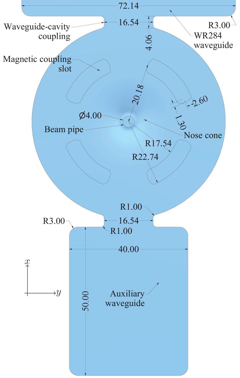
Optimizing the coupling of the RF feed (reduced WR284 waveguide: 72.136 mm by 20 mm) is critical since only a 5 kW (peak) pulsed solid-state amplifier is intended to be used. An - projection of the second cell, the magnetic coupling slots, and waveguide feed is shown in Fig. (5). It also features a coupling structure at the bottom of the cavity, thus minimizing any dipole fields induced by the coupling structure of the RF feed [19]. Optimizing the coupling between the top waveguide and the second cell is done primarily by varying the width of the waveguide coupler (16.54 mm in Fig. (5)), which is the same for both the bottom and top coupler structure. RF power at a frequency of 3 GHz can propagate freely through the top waveguide with a width of 72.136 mm, the bottom auxiliary waveguide width is smaller, resulting in a higher cut-off frequency, preventing it from absorbing RF power.
| Parameter | Value | Unit |
|---|---|---|
| Unloaded Q | 8754 | |
| Operating frequency | 2998.46 | MHz |
| Mode separation | 17.96 | MHz |
| Structure filling time | 0.465 | s |
| RF power | 5 | kW |
| Shunt impedance () | 1.71 | M |
| Duty cycle | 1 | % |
| Repetition frequency | 1 | kHz |
| Average RF power | 50 | W |
| Peak on-axis E field | 8.3 | MV m-1 |
| Peak surface E field | 25 | MV m-1 |
| Field balance | 1.0 : 1.0 | |
| Cooling water temperature | 298.15 | K |
| Steady state temperature | 300.65 | K |
Typically, the edges of the coupling slots (‘waveguide-cavity coupling’ in Fig. (5)) are also optimized in order to minimize the maximum surface magnetic field along the coupling slot, which in turn reduces the steady-state temperature of the coupling slots’ edges. This temperature is typically lowered as the blend radius closer to the cell is increased [20]. Finally, the inner radius, outer radius, and the rounding of the magnetic coupling slots are optimized in such a way that the two cavities are coupled sufficiently and the power dissipation along the edges of the slots does not lead to excessive heating (see Fig. (5)).
Optimizing the coupling slots has consequences for the separation of the frequencies of the two resonant modes. The mode-separation , where for the presented structure is always the higher frequency of the two, has been maximized by variation of the sizes and shapes of the coupling slots. A mode separation of MHz is obtained, with MHz and an unloaded quality factor , resulting in a 1/ filling time of s. The structure will be limited to operation at 1 kHz because of the repetition frequency of the ionization laser and the MOT loading rate.
3.3 Waveguides and higher-order-modes
The design of the proposed DC/RF source features a double coupling design at the second cell. One of these couplers is connected to a WR284 waveguide with a standard length (72.136 mm) and adjusted width of 20 mm. The auxiliary port may also be used as a pump opening and can potentially house a pick-up probe [21].
The auxiliary waveguide has the same width as the feed waveguide, i.e. 20 mm (the same width as the second cell) but a smaller length (40 mm, see Fig. (5)), in order to ensure that the RF power can not propagate in the auxiliary waveguide (f GHz). The suppression of the dipole field is not perfect, resulting in a minor dipole kick due to the power flow from the single waveguide. It however has negligible influence on the beam quality as will be shown in Sec. (4).
3.4 Electromagnetic field distribution
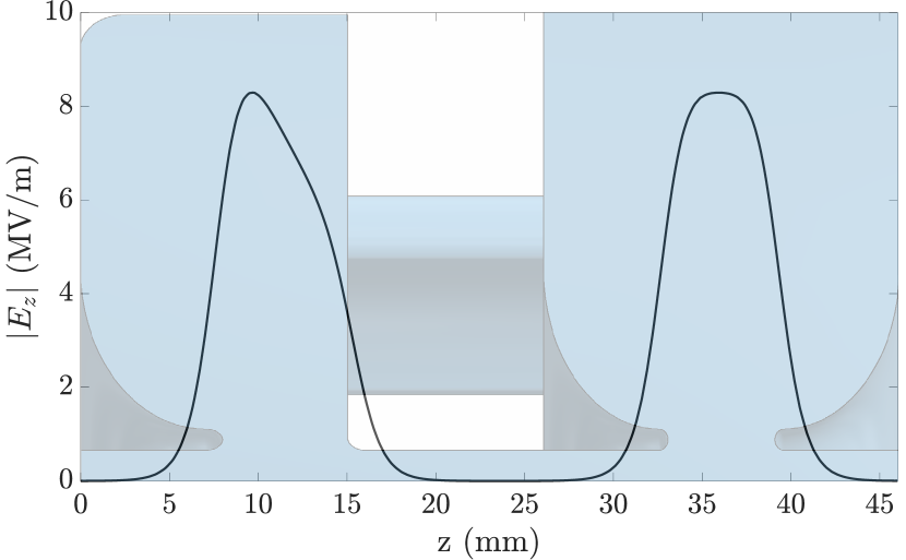
The electromagnetic fields were calculated using the frequency-domain solver in cst microwave studio [18] with a simulated peak input power of 5 kW being delivered to the structure through the feed waveguide (50 W average power at a repetition frequency of 1 kHz with a 10 s pulse length, see Table (1)). The resulting electric field and the transverse magnetic field are shown in Fig. (6).
The on-axis electric field for a peak input power of 5 kW is shown in Fig. (7) along with an impression of the vacuum geometry of the RF accelerator. It is clearly seen that the field profile at the first cell is deformed due to the asymmetric shape of cavity I. On-axis field strengths in excess of 8 MV/m are obtained, which is sufficient for the purposes of this source. The maximum surface electric field strengths are 25 MV/m on the tip of the nose cones, well below breakdown field strengths for S-band normal-conducting copper cavities [22, 23].
3.5 Thermal analysis
During steady state operation with a peak input power of 5 kW, RF pulses with a duration of 10 s, and repetition frequencies of 1 kHz, an average power of 50 W will be dissipated in the RF structure at the resonant frequency. The steady state heating of the RF structure is investigated using cst microwave studio by calculating the power dissipation at the resonant frequency and using the resulting power loss density to calculate the final temperature of the structure for some given duty cycle.
The structure is modeled as pure copper with a thermal conductivity of 401 W K-1m-1 and a specific heat of 390 J K-1kg-1. Fig. (8) shows the steady state temperature of the actively cooled system with the color bar indicating the local temperature.
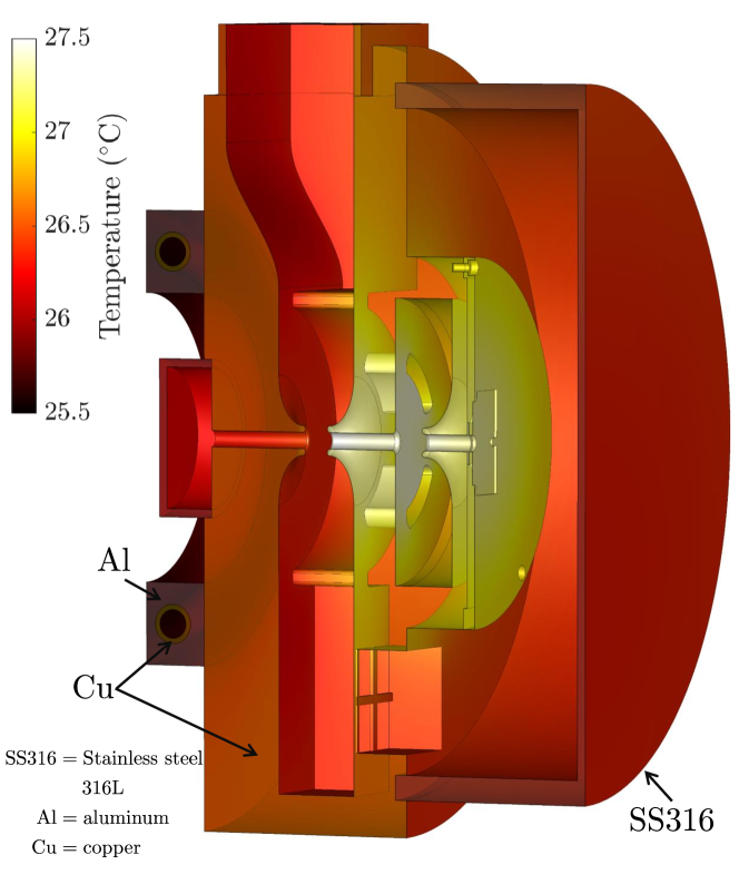
Fig. (8) shows the copper body of the RF structure along with a stainless steel CF160 pipe on the left side, which houses the accelerator module used for the static extraction field, additionally a stainless steel CF40 pipe is simulated on the right as the beginning of the beam pipe system, the cooling channel can be seen here, placed concentrically around the pipe.
In the simulation the boundary conditions of the domain are open and the system is cooled by a hollow toroidal copper cooling channel with an inner radius of 7 mm, covered by an aluminum encasing. Water at a temperature of 25 ∘C flows at a rate of 6 L min-1, which results in a convective heat transfer coefficient of 11103 W m-2 K-1. In this situation the temperature change from the nose cone of the first cell to the right nose cone of the second cell is approximately +1 K. For an ideal copper pillbox cavity oscillating in TM010 mode this would result in a frequency shift of kHz/K at 3 GHz [24]. This gives rise to phase shifts in the order of 3 mrad.
4 PARTICLE TRACKING SIMULATIONS
The simulations presented in this section have all been performed using the general particle tracer (GPT) software [25]. A realistic beamline has been simulated which consists of a set of anti-Helmholtz configured magnetic coils (forming the MOT coils) [26], a DC accelerator module [16], and the -cell RF structure as shown in Fig. (1, 2). Detailed fieldmaps of the DC accelerator module and the RF structure are used and 1.6 fC - 16 fC electron bunches are simulated. The MOT coils used in the simulation have a total of 196 windings each and are supplied with a current of 9.0 A (front coil) and -11.3 A (back coil). Each has a radius of 90 mm and are separated by 180 mm. This creates a magnetic field gradient of mT/m. The DC accelerator that extracts the electron bunches generates a static field of 1.4 MV/m across a gap of 19.2 mm. The electron bunch is extracted from a (rms) ionization volume at a distance of 7.5 mm from the grating chip. The initial isotropic momentum spread is thermal with an electron temperature K.
The ionization process is simulated by creating electrons in the ionization volume according to a Gaussian distribution at a 1 ps rms time scale [15]. Coulomb interactions are taken into account between all individual electrons. The interaction between the electrons and the rubidium ions is neglected in this simulation, which is justified by the fact that the electrons leave the DC field after a fraction of the inverse plasma frequency ns. This implies that the bunches are not significantly affected through disorder-induced heating [27].
The average electric field experienced by the electrons in the simulation and their average kinetic energy is shown in Fig. (9) as a function of the longitudinal position .
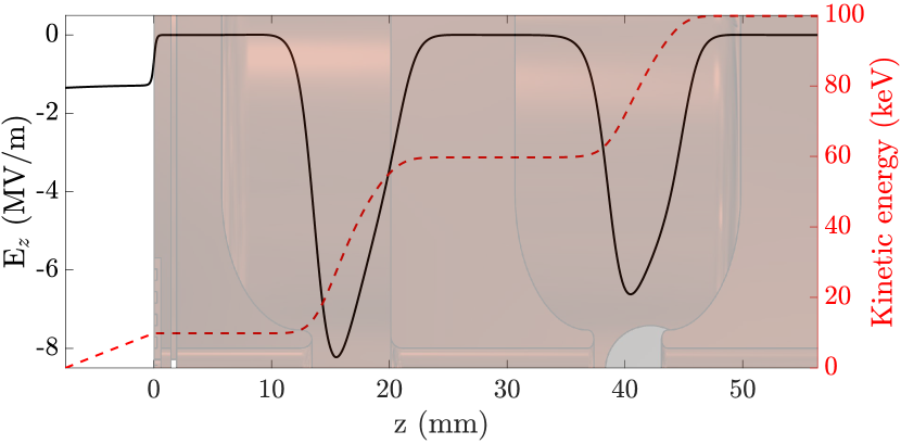
Electrons are accelerated up to 10 keV in the static accelerator field which is located in the white region of the figure. The first and second cell of the RF structure add approximately 50 keV and 40 keV respectively. The difference in experienced field strength and corresponding acceleration in the cells is due to the finite travel time between them, resulting in a phase advance.
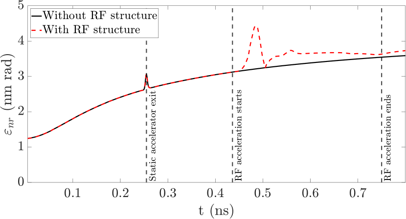
In order to check the influence of the RF structure on the beam quality a simulation is done without the RF fields enabled in the simulation. Comparing the normalized emittance in a transverse direction as a function of the simulation time then gives an indication of the extent with which th RFe accelerator structure influences the transverse bunch dynamics, this is shown in Fig. (10).
Here the normalized transverse emittance in a co-rotating frame is shown,
which has the advantage that artificial emittance growth due to strong and coupling whilst traversing solenoid fields is omitted. This makes it easier to observe the actual emittance growth at the source better [25].
This variable is plotted as a function of simulation time for simulations with and without an RF structure, signified by the dashed red curve and the solid black curve respectively. The exit of the static accelerator is marked by the vertically dashed lines, as well as the beginning and ending of the RF acceleration. These simulations show that there is some minor growth of the beam emittance due to the RF structure: pm rad at the end of the RF acceleration with respect to the non-accelerated case. This implies that the emittance growth in this simulation is driven by non-linear space charge forces, acting mainly on the periphery of the bunch.
The figure of merit to optimize for this source is the reduced transverse brightness, defined as:
| (2) |
where is the total bunch charge and the normalized transverse emittance in the -direction. Bunches with an initial Gaussian distribution in the longitudinal and transverse direction are not the most optimal in terms of suppressing space charge driven emittance growth. This results in a reduced transverse brightness that does not benefit greatly from an increased bunch charge, as this exacerbates these forces. Space charge driven transverse emittance growth can be reduced by increasing the initial longitudinal length of the bunch, resulting in a larger value for the reduced transverse brightness. For 1.6 fC Gaussian bunches this is shown by the solid black and dashed red lines with dots in Fig. (11).
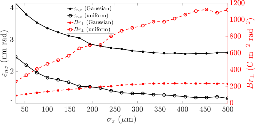
This figure shows the benefit of increasing the bunch length for a fully Gaussian shaped bunch with an initial rms transverse size of 30 m, resulting in a smaller reduced transverse emittance.
Other distributions are more suited to handle space charge driven quality degradation. Bunches with a uniform disk-like profile in the transverse plane (with a radius of 30 m) and a Gaussian longitudinal density profile benefit much more from an increase in the initial rms longitudinal bunch length, as is shown by the solid black and dashed red lines with circles in Fig. (11). Realizing these initial distributions would however require additional optics like spatial light modulators
In fig. (12) the resulting reduced transverse brightness is plotted when scanning the total bunch charge up to 16 fC for transversely Gaussian and transversely uniform bunches, both with an initial rms length of 500 m (Gaussian). From this figure it is seen that the bunches with a uniform transverse density profile perform better, but reach their best performance at a bunch charge at around 1.1 fC with an accompanying of approximately 1060 C m-2 rad-2, whereas the fully Gaussian bunch has its optimum at a bunch charge of roughly 3.7 fC with a corresponding of roughly 272 C m-2 rad-2.
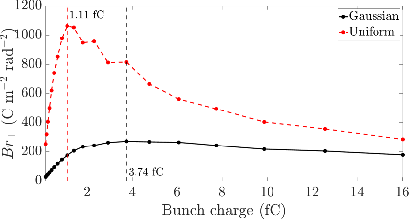
Additional optimization of, among other things, the initial RF phase of the accelerator structure, the field balance, initial bunch length, etc. might result in better performance. It is evident however, from Fig (11) and (12), that a distribution which more closely resembles a homogeneously filled disk in the transverse direction will outperform a simple 3D Gaussian distribution.
5 SUMMARY
The design, optimization, and particle tracking simulations of a compact 1-cell, standing wave RF structure was presented. The RF structure, combined with the UCES [8], results in a hybrid DC/RF structure which was readily proposed [12]. The system presented in this article is capable of accelerating electrons up to 100 keV with minimal normalized transverse emittance growth. The structure is optimized to be resonant at approximately 2.99855 GHz and only requires 5 kW peak input power, easily supplied by commercially available solid-state amplifiers. Thermal simulations show that operation at a repetition frequency of 1 kHz can be sustained with easily manageable temperature rises.
The quality degradation of the electron bunches is observed primarily in the static extractor field of the source, the RF structure itself adds little to the degradation of the bunch. By using a more complex initial transverse distribution of the created bunches, the reduced transverse brightness of this source can exceed the performance of a conventional RF photosource, potentially reaching a reduced transverse brightness of C m-2 rad-2.
Acknowledgments
The author would like to thank A. Rajabi, T.G. Lucas, and W.F. Toonen for their support and fruitful discussions, additionally, thanks to E. Rietman, M. van der Sluis, H. van Doorn, and H. van den Heuvel for their expert technical assistance. This publication is part of the project ColdLight: From laser-cooled atoms to coherent soft X-rays (with project number 741.018.303 of the research programme ColdLight) which is (partly) financed by the Dutch Research Council (NWO).
References
- [1] B. J. Claessens, S. B. Van Der Geer, G. Taban, E. J. D. Vredenbregt, O. J. Luiten, Ultracold electron source, Phys. Rev. Lett. 95 (16) (2005) 1–4. doi:10.1103/PhysRevLett.95.164801.
- [2] G. Taban, M. P. Reijnders, B. Fleskens, S. B. van der Geer, O. J. Luiten, E. J. D. Vredenbregt, Ultracold electron source for single-shot diffraction studies, Europhysics Letters 91 (4) (2010) 46004. doi:10.1209/0295-5075/91/46004.
- [3] A. J. McCulloch, D. V. Sheludko, S. D. Saliba, S. C. Bell, M. Junker, K. A. Nugent, R. E. Scholten, Nat. Phys.doi:doi.org/10.1038/nphys2052.
- [4] W. J. Engelen, M. van der Heijden, D. J. Bakker, E. J. D. Vredenbregt, O. J. Luiten, High-coherence electron bunches produced by femtosecond photoionization., Nat. Commun. 4 (2013) 1693. doi:10.1038/ncomms2700.
- [5] A. J. McCulloch, D. V. Sheludko, M. Junker, R. E. Scholten, High-coherence picosecond electron bunches from cold atoms., Nat. Commun. 4 (2013) 1692.
-
[6]
W. Engelen, E. Smakman, D. Bakker, O. Luiten, E. Vredenbregt,
Effective
temperature of an ultracold electron source based on near-threshold
photoionization, Ultramicroscopy 136 (2014) 73–80.
doi:https://doi.org/10.1016/j.ultramic.2013.07.017.
URL https://www.sciencedirect.com/science/article/pii/S0304399113002039 - [7] R. W. Speirs, C. T. Putkunz, A. J. McCulloch, K. A. Nugent, B. M. Sparkes, R. E. Scholten, Single-shot electron diffraction using a cold atom electron source, J. Phys. B At. Mol. Opt. Phys. 48 (21) (2015) 214002. doi:10.1088/0953-4075/48/21/214002.
-
[8]
J. G. H. Franssen, T. C. H. de Raadt, M. A. W. van Ninhuijs, O. J. Luiten,
Compact
ultracold electron source based on a grating magneto-optical trap, Phys.
Rev. Accel. Beams 22 (2019) 023401.
doi:10.1103/PhysRevAccelBeams.22.023401.
URL https://link.aps.org/doi/10.1103/PhysRevAccelBeams.22.023401 - [9] A. H. Zewail, Four-dimensional electron microscopy, Science 328 (5975) (2010) 187–193. doi:10.1126/science.1166135.
- [10] B. H. Schaap, S. Schouwenaars, O. J. Luiten, A raman quantum free-electron laser model, Physics of Plasmas 29 (11) (2022) 113302. doi:10.1063/5.0106439.
- [11] R. Shiloh, T. Chlouba, P. Hommelhoff, Experimental considerations in electron beam transport on a nanophotonic chip using alternating phase focusing, Journal of Vacuum Science&Technology B 40 (2022) 010602. doi:10.1116/6.0001598.
-
[12]
S. van der Geer, E. Vredenbregt, O. Luiten, M. de Loos,
An ultracold electron
source as an injector for a compact sase fel, Journal of Physics B: Atomic,
Molecular and Optical Physics 47 (23) (nov 2014).
doi:10.1088/0953-4075/47/23/234009.
URL https://doi.org/10.1088/0953-4075/47/23/234009 -
[13]
C. C. Nshii, M. Vangeleyn, J. P. Cotter, P. F. Griffin, E. A. Hinds, C. N.
Ironside, P. See, A. G. Sinclair, E. Riis, A. S. Arnold,
A surface-patterned chip as a
strong source of ultracold atoms for quantum technologies, Nature
Nanotechnology 8 (5) (2013) 321–324.
doi:10.1038/nnano.2013.47.
URL http://dx.doi.org/10.1038/nnano.2013.47 - [14] J. G. H. Franssen, T. L. I. Frankort, E. J. D. Vredenbregt, O. J. Luiten, Pulse length of ultracold electron bunches extracted from a laser cooled gas, Struct. Dyn. 4 (4) (2017) 044010. doi:10.1063/1.4978996.
- [15] T. C. H. de Raadt, J. G. H. Franssen, O. J. Luiten, Sub-picosecond ultracold electron source, Physical Review Letters (2023) to be published.
- [16] J. G. H. Franssen, An ultracold and ultrafast electron source, Ph.D. thesis, Eindhoven University of Technology, dissertation (May 2019).
- [17] C. Krenn, W. Scherf, O. Khait, M. Musso, L. Windholz, Stark effect investigations of resonance lines of neutral potassium, rubidium, europium and gallium, Zeitschrift für Physik D Atoms, Molecules and Clusters 41 (4) (1997) 229–233. doi:10.1007/s004600050315.
-
[18]
Dassault Systèmes,
CST
studio suite.
URL https://www.3ds.com/products-services/simulia/?utm_source=cst.com&utm_medium=301&utm_campaign=products - [19] M. Chae, J. Hong, Y. W. Parc, I. Ko, S. Park, H. Qian, W. Huang, C. Tang, Emittance growth due to multipole transverse magnetic modes in an rf gun, Physical Review Special Topics - Accelerators and Beams 14 (10 2011). doi:10.1103/PhysRevSTAB.14.104203.
- [20] L. Xiao, R. Boyce, D. Dowell, Z. Li, C. Limborg-Deprey, J. Schmerge, Dual feed rf gun design for the lcls, in: Proceedings of the 2005 Particle Accelerator Conference, 2005, pp. 3432–3434. doi:10.1109/PAC.2005.1591495.
- [21] D. Dowell, E. Jongewaard, J. Lewandowski, C. Limborg, Z. Li, J. Schmerge, A. Vlieks, J. Wang, L. Xiao, The development of the linac coherent light source rf gun, ICFA Beam Dynamics Newsletter No. 46 46 (2008) 162.
-
[22]
A. Degiovanni, R. Bonomi, M. Garlasché, S. Verdú-Andrés, R. Wegner,
U. Amaldi,
High
gradient rf test results of s-band and c-band cavities for medical linear
accelerators, Nuclear Instruments and Methods in Physics Research Section A:
Accelerators, Spectrometers, Detectors and Associated Equipment 890 (2018)
1–7.
doi:https://doi.org/10.1016/j.nima.2018.01.079.
URL https://www.sciencedirect.com/science/article/pii/S0168900218301128 - [23] A. Vnuchenko, D. Pereira, B. Martinez, S. Benedetti, N. Catalan Lasheras, M. Garlasch, A. Grudiev, G. McMonagle, S. Pitman, i. Syratchev, M. Timmins, R. Wegner, B. Woolley, W. Wuensch, F.-G. Angeles, High-gradient testing of an s-band, normal-conducting low phase velocity accelerating structure, Physical Review Accelerators and Beams 23 (08 2020). doi:10.1103/PhysRevAccelBeams.23.084801.
-
[24]
D. Pozar, Microwave
Engineering, Addison-Wesley series in electrical and computer engineering,
Addison-Wesley, 1990.
URL https://books.google.nl/books?id=0XLFQgAACAAJ - [25] B. van der Geer, M. de Loos, General Particle Tracer - http://www.pulsar.nl.
-
[26]
J. P. McGilligan, P. F. Griffin, R. Elvin, S. J. Ingleby, E. Riis, A. S.
Arnold, Grating chips for
quantum technologies, Scientific Reports 7 (1) (Mar 2017).
doi:10.1038/s41598-017-00254-0.
URL http://dx.doi.org/10.1038/s41598-017-00254-0 -
[27]
T. Killian, T. Pattard, T. Pohl, J. Rost,
Ultracold
neutral plasmas, Physics Reports 449 (4) (2007) 77–130.
doi:https://doi.org/10.1016/j.physrep.2007.04.007.
URL https://www.sciencedirect.com/science/article/pii/S0370157307001937