Terahertz bolometric detectors based on graphene field-effect transistors with the composite h-BN/black-P/h-BN gate layers using plasmonic resonances
Abstract
We propose and analyze the performance of terahertz (THz) room-temperature bolometric detectors based on the graphene channel field-effect transistors (GC-FET). These detectors comprise the gate barrier layer (BL) composed of the lateral hexagonal-Boron Nitride black-Phosphorus/ hexagonal-Boron Nitride (h-BN/b-P/h-BN) structure. The main part of the GC is encapsulated in h-BN, whereas a short section of the GC is sandwiched between the b-P gate BL and the h-BN bottom layer. The b-P gate BL serves as the window for the electron thermionic current from the GC. The electron mobility in the GC section encapsulated in h-BN can be fairly large. This might enable a strong resonant plasmonic response of the GC-FET detectors despite relatively lower electron mobility in the GC section covered by the b-P window BL. The narrow b-P window diminishes the Peltier cooling and enhances the detector performance. The proposed device structure and its operation principle promote elevated values of the room-temperature GC-FET THz detector responsivity and other characteristics, especially at the plasmonic resonances.
I Introduction
The favorable band alignment of the graphene channel (GC) and the black-ArsenicxPhosphorus1-x (b-AsP) layers [1, 2, 3, 4] enables new opportunities for electron and optoelectronic device applications. In particular, we recently proposed the terahertz (THz) bolometric detectors based on the field-effect transistors (FETs) with the b-AsP gate barrier layer (BL) and the metal gate (MG) [5, 6]. The operation of such bolometric detectors is associated with the heating of the two-dimensional electron (hole) system (2DEG) by the THz radiation resulting in the reinforcement of the thermionic electron emission from the GC to the MG via the b-AsP BL. The resonant excitation of the plasmonic oscillations in the GC [7, 8, 9] can result in a substantial rise of the electron heating efficiency and can lead to improvement of the detector characteristics, in particular, enhancement of the detector responsivity. However, the plasmonic resonances are sensitive to electron scattering, limiting the sharpness of the resonances and the responsivity peaks. This problem is linked to the prospects of elevating the room temperature mobility of the GCs contacted with the b-AsP BLs.
In this paper, we propose and evaluate the room-temperature THz bolometric detectors based on the GC-FETs, in which the thermionic electron current passes through a relatively narrow b-P collector window in the primarily h-BN gate BL.
The main part of the GC/BL interface is made of h-BN, so the GC exhibits higher electron mobility in comparison with the GC covered by the b-P gate BL [10, 11, 12, 13, 14, 15].
Using the composite h-BN/b-AsP/h-BN gate BL, one can improve the GC-FET detector performance due to:
(i) a substantial decrease in the plasmonic oscillations damping;
(ii) a weaker hot electron energy flux from the GL via the b-P collector window resulting in the diminishing of the Peltier cooling of the 2DEG [16] because of a smaller length of the b-P section of the BL.
As shown in the following, these features of the GC-FETs with the composite gate BL enable a marked enhancement of the detector performance.
II GC-FET bolometric detector device structure
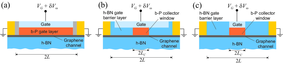
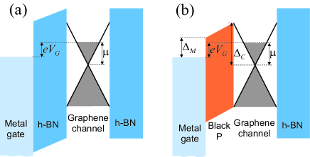
Figure 1 shows the structures of the GC-FET bolometric detectors with different BLs and MGs. The structure of the GC-FET with the uniform b-P gate BL [see Fig. 1(a)] was considered previously [8, 15]. Here, we focus on the GC-FET bolometric detectors operating at room temperature with the composite BLs, schematically shown in Fig. 1(b). The devices with the structures seen in Fig. 1(c) are briefly discussed in the Comments section. The structure of the GC-FET bolometric detectors under consideration [see Fig. 1(b)] comprises the n-doped GC sandwiched between the substrate (h-BN) and the h-BN gate BL with a narrow b-P window. This structure is covered by the MG and supplied by the side contacts (corresponding to the FET source and drain). The length of the collector window is smaller than the length of the GC . Figure 2 shows these GC-FET bolometric detectors band diagram (in the direction perpendicular to the layers). The relatively low energy barrier for the electrons in the GL enables thermionic emission (in the region ) above the energy barrier at the GC/b-P interface. In contrast, this energy barrier in the regions is fairly high, preventing electron emission from this section of the GC.
We assume that the sufficiently high GC doping level provides at the bias voltage the flat-band condition . Here and are the pertinent band offsets, is the electron Fermi energy in the GC, where cm/s is the electron velocity in GCs, is the donor density in the GC (or the density of the remote donors in the substrate near the GC), and is the Planck constant. In the GC-FETs under consideration with the Al MG, meV and meV, so that meV, as shown in Table I. The latter occurs at cm-2 (see Ref. [8] and the references therein). When , the bottom of the b-P BL conduction band is somewhat inclined, as shown in Fig. 2(b). Below we consider the GC-FETs with not too thin BLs in the range of relatively low bias voltages, so that the electron tunneling through the BLs is negligible.
Apart from the bias voltage , the signal voltage generated by the THz radiation received by an antenna is applied between the GL and the MG. Here and are the amplitude and frequency of the THz signal. This connection corresponds to the contact of one antenna lead with the MG and another with both the GC-FET side contacts. The signal voltage excites the ac current along the GC, resulting in electron heating in the GC. The latter stimulates thermionic emission from the GC over the b-P section of the BL.
III Rectified current
The variation of the rectified thermionic gate current, , associated with the incoming THz signal (and averaged over its period and serving as the detector output signal) is presented in the following form:
| (1) |
Here , is the maximal value of the current density from the GC to the MG via the b-P BL, is the lattice temperature, is the averaged electron effective temperature variation, and is the GC width. The maximal electron current density is given by , where is the electron density in the GC, is the electron try-to-escape time, is the electron Fermi energy, and is the electron charge.
IV Electron energy balance in the GC and ac effective temperature
The spatial distribution (along the axis ) of , is described by the one-dimensional electron heat transport equation, which for the device structure under consideration is presented in the following form [15]:
| (2) |
Here is the electron thermal conductivity in the GC per electron (this corresponds to the Wiedemann-Franz relation), is the electron energy relaxation time in the GC, is the Joule power (per GC area unit) associated with the signal electric field, , along the GC caused by the signal voltage at the side contacts and and amplified by the plasmonic effect, , are the Drude ac and dc conductivities, and is the electron scattering frequency in the GC. Due to the smallness of the collector window length, we disregard the energy flux of the electrons transferring from the GC into the MG via this window (i.e.,the Peltier cooling) [9, 15, 16] in comparison with the electron energy relaxation on phonons in the whole GC [17, 18, 19, 20, 21] and the heat absorbed by the side contacts (due to a high electron heat conductivity in GCs [22, 23]).
The quantity is the square of ac electric field modulus averaged over the oscillations. Setting the boundary condition of the ac potential as
| (3) |
and accounting for the excitation of plasmonic oscillations in the gated two-dimensional electron systems (neglecting the role of the short GC b-P region) one can obtain (see Appendix A)
| (4) |
Here and are the effective wavenumber and the plasmonic frequency (corresponding to the symmetric conditions at the contacts), respectively, is the dielectric constant of the BLs, is the GL thicknesses. The second term in the left-hand side of Eq. (2) is associated with the electron energy relaxation due to the interaction with phonons (mainly with the GC and interface phonons [17, 18, 19, 20, 21]), whereas the term in the right-hand side describes the Joule heating by the ac electric field induced by the potential variations at the side contacts (i.e., by the THz radiation).
Solving Eq. (2) with the boundary conditions
| (5) |
we obtain the following spatial distribution:
| (6) |
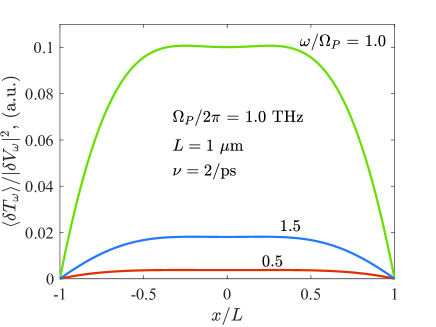
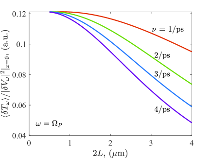
Figure 3 shows the spatial distributions of the temperature signal component obtained using Eq. (6) for different ratios, , of the signal frequency and the plasmonic frequency. It is seen that the deviation of the signal frequency from the plasmonic frequency leads to a marked weakening of the electron heating. The dependences of the (in the GC center) versus the GC length for different values of the electron collision frequency are plotted in Fig. 4. The behavior of these plots is associated with the specifics of the ac electric field distribution (this field is a relatively small in the GC center leading to a decrease of the average field with increasing , and the dependence of the electron heat conductivity on ). As follows from Eq. (6), , where
| (7) |
and the parameter characterize the electron system cooling at the side contacts. The factor and, hence, exhibit a pronounced variation with varying and (via the dependence of on and ), which leads to the features of Fig. 4.
| (meV) | (meV) | (meV) | (m) | (m) | W (nm) | (THz) | (ps) | (ps) | (ps) |
|---|---|---|---|---|---|---|---|---|---|
| 225 | 85 | 140 | 1.0 | 0.05 - 0.15 | 32 - 72 | 1.0 - 1.5 | 0.25 - 1.0 | 10 | 10 |
V Detector responsivity
Equations (1) and (6) result in
| (8) |
We use the following definition of the GC-FET bolometric detector voltage responsivity: , where is the load resistance, and is the THz power collected by the detector antenna.
The dark current is given by [15]
| (9) |
where . Here we accounted for that at . Considering Eq. (9), we find that at (where ),
| (10) |
Accounting for that the antenna aperture , where is the THz radiation wavelength and is the antenna gain [24], for the relation between and the collected power we obtain , where is the speed of light in vacuum. Using the latter and invoking Eq. (7), we obtain
| (11) |
where
| (12) |
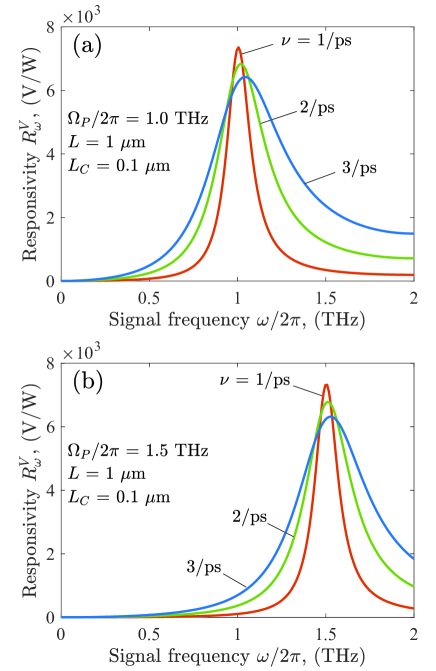
is the responsivity characteristic value. Here is the electron mobility in the GC. At the denominator in the right-hand side describes the resonant frequency dependence of [with maxima of the latter at , is the resonance index]. The quantity is equal to the maximal voltage responsivity at the fundamental resonance [see Eq. (7)]. It is instructive that is independent of the length of the collecting window and the try-to-escape time .
Using the device structure parameters for the detector structure with 2/ps, m, m, and (other parameters are listed in Table I), and accounting for Eqs. (9) - (11), for the resonant responsivity we obtain V/W.
VI Detector noise equivalent power and dark current limited detectivity
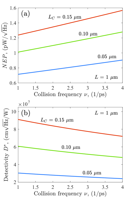
Using Eqs. (9) and (11), we arrive at the following expressions for the GC-FET noise equivalent power (NEP) and the dark-current-limited detectivity () at the fundamental plasmonic resonance ():
| (13) |
| (14) |
respectively, where
The estimates for and of the GC-FET detector with the same parameters as those used for the estimation of yield pW/ and cm/W. These values are about or exceeding the characteristics of other uncooled THz bolometers (see, for example, Refs. [25] and [26]).
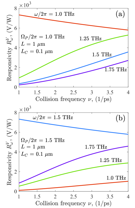
Figure 7 shows and as functions of calculated for the GC-FETs with different lengths, , of the collector window.
VII Comments
Calculating Eq. (9), we disregarded the variation of with increasing bias voltage at not too large bias voltages, . For and the same other parameters as above, meV and meV. Hence, at , one obtains .
According to Eq. (9), the dark current , where is given by Eq. (10). Taking this into account, in particular, for the ratio of in a wide range of and at given by Eq. (14) we obtain . It is worth noting that at smaller gate voltages , the detector detectivity might be limited not by the dark current, but by the Johnson-Nyquist (J-N) noise (see, for example, Ref. [27]). Indeed, the J-N noise is , while the dark current noise is , for the ratio of the pertinent detectivity values we obtain . However, the optimum value of the gate bias would also depend on the exposure level and the readout circuitry (see Ref. [28] for more details).
The present study does not include the consideration of high bias voltages since, in this case, the ”thermionic model” becomes invalid and the electron tunneling from the GC through the b-P BL must be accounted for.
The parameters assumed above correspond to the electron mobility in the GC in the range of cm2/Vs. For the chosen electron density, these values for the room temperature mobility in the GCs, a substantial part of which is encapsulated by b-BN, are fairly realistic (see, for example, Refs. [11, 12, 13]). The elevated values of the GC room-temperature mobility and, hence, decreased electron collision frequencies, can be also achieved in the GC-FET structures with the sections of the WSe2 gate BL [29] replacing the pertinent h-BN sections. Similar GC-FET bolometric detectors can comprise the b-AsP or b-As central BL sections.
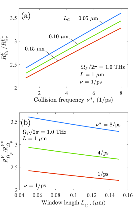
Below we compare the voltage responsivities, and , of the GC-FET detectors with the composite h-BN/b-P/h-BN gate BL and the uniform b-P gate BL [15] at , assuming that the load resistances are equal to their terminal resistances for both detectors. For their responsivities, we obtain the plots in Fig. 8 (the asterisk marks the responsivity of the GC-FETs with the b-P gate BL). Figure 8(a) shows the ratio of the responsivities , as a function of the collision frequency, , in the GC-FETs with the b-P gate BL, for the the collision frequency in the FET with the composite BL equal to 1/ps and different b-P window BL length values . Figure 8(b) shows the dependence of these responsivities on calculated for different . As seen in Fig. 8, the incorporation of the composite gate BL might provide a marked enhancement of the GC-FET detector performance. The fact that the ratio increases with increasing relatively slowly is attributed to a weakening of the electron cooling at the side contacts when rises.
When electron collision frequency in the GC central (collector window) section , the contribution of this section to the Joule heating can be marked. This might limit the applicability of the model used above to a relatively small .
Now we compare the net Joule power produced in the side sections, , and in the central section, , at the fundamental plasmonic resonance for the limiting case . Equations (A3) and (A4) (see Appendix A) give rise to the following estimate of the ratio:
| (15) |
At the fundamental plasmonic resonance (), assuming that , Eq. (15) yields the estimate:
| (16) |
This implies that the simplification made in Sec. IV is justified when . Here and are the electron mobilities in the pertinent sections of the GC. In the case of the h-BN/b-P/h-BN composite BL at room temperature, one can set cm2/Vs [10], and cm2/Vs [11] (i.e., /ps as was used for the dependences in Figs. 3 - 5). The latter values correspond to the condition , which was satisfied in the above calculations. At a small and a large , the electron heating in the middle section can be not too small. However, this circumstance can be beneficial leading to the enhancement of the GC-FET bolometric detectors under consideration.
Our device model intended for the GC-FET bolometric detectors with the composite BL assumes that the effect of Peltier cooling is weaker than the electron energy relaxation due to the interaction with phonons. The pertinent condition means . Using the parameters listed in Table I, we arrive at the following criterion . If , this condition is not burdensome.
The effect of the electron thermal transport along the GC and of the side contacts cooling can be diminished in the GC structures shown in Fig. 1(c). In the structure with a short b-P window BL and a short MG shown in Fig. 1(c), the spacing can be relatively large without sacrificing the plasmonic frequency . This is because the ungated GCs can exhibit rather large even at relatively long . The device model of this GC-FET bolometric detector is more complex and requires a separate study.
Conclusions
We predicted that implementation of the GC-FET bolometric detectors with the composite h-BN/b-P/h-BN gate BL having a narrow b-P collector window could substantially enhance the detector performance in comparison with the GC-FETs with the uniform b-P gate BL, especially invoking the plasmonic resonances.
Author’s contributions
All authors contributed equally to this work.
Acknowledgments
The work at RIEC, UoA, and UB was supported by the Japan Society for Promotion of Science (KAKENHI Nos. 21H04546, 20K20349), Japan and the RIEC Nation-Wide Collaborative research Project No. R04/A10, Japan. The work at RPI was supported by AFOSR (contract number FA9550-19-1-0355).
Conflict of Interest
The authors declare no conflict of interest.
Data availability
All data that support the findings of this study are available within the article.
Appendix A.
The signal component of the potential in the gated GC is governed by the following equations [6, 15]:
| (A1) |
at , and
| (A2) |
at . Here , , and and are the electron collision frequencies in the pertinent section of the GC. Apart from the boundary conditions (3), these equations are supplemented by the conditions of the potential continuity at .
In the case , neglecting the contribution of a narrow region , i.e., extending the validity of Eq. (A1) all over the whole GC, we obtain
| (A3) |
This equation leads to Eq. (4) in the main text.
The electron collision frequency in the b-P collector window region differs from that, , in the main part of the GC-FET structure, where it is determined by the GC-n-BN interfaces. In the devices under consideration, the ratio can be rather large. Solving Eqs. (A1) and (A2), we obtain the spatial potential distribution in the region coinciding with with that given by Eq. (A3), while the distribution in the region is given by
| (A4) |
If , Eqs. (A3) and (A4) coincide, and Eqs. (4) -(12) are valid for a wide range of ratio .
References
- [1] Xi Ling, H. Wang, S. Huang, F. Xia, and M. S. Dresselhaus, “The renaissance of black phosphorus,” PNAS 122, 4523 (2015).
- [2] F. Xia, H. Wang, and Y. Jia, “Rediscovering black phosphorous as an anisotropic layered material for optoelectronics and electronics,” Nat. Commun. 5, 4458 (2014).
- [3] Y. Cai, G. Zhang, and Y.-W. Zhang, “Layer-dependent band alignment and work function of few-layer phosphorene,” Sci. Rep. 4, 6677 (2015).
- [4] F. Liu, X. Zhang, P. Gong, T. Wang, K. Yao, S. Zhu, and Y. Lu, “Potential outstanding physical properties of novel black arsenic phosphorus As0.25P0.75/As0.75P0.25 phases: a first-principles investigation,” RSC Adv. 12, 3745 (2022).
- [5] V. Ryzhii, C. Tang, T. Otsuji, M. Ryzhii, V. Mitin, and M. S. Shur, “Hot-electron resonant terahertz bolometric detection in the graphene/black-AsP field-effect transistors with a floating gate,” J. Appl. Phys. 133, 174501 (2023).
- [6] V. Ryzhii, C. Tang, T. Otsuji, M. Ryzhii, V. Mitin, and M. S. Shur, “Effect of electron thermal conductivity on resonant plasmonic detection in the metal/black-AsP/graphene FET terahertz hot-electron bolometers,” Phys. Rev. Appl. …, … (2023)- in press [arXiv:2303.08492 (2023)].
- [7] V. Ryzhii, A. Satou, and T. Otsuji, “Plasma waves in two-dimensional electron-hole system in gated graphene heterostructures,” J. Appl. Phys. 101, 024509 (2007).
- [8] A. V. Muraviev, S. L. Rumyantsev, G. Liu, A. A. Balandin, W. Knap, and M. S. Shur, “Plasmonic and bolometric terahertz detection by graphene field-effect transistor,” Appl. Phys. Lett. 103, 181114 (2013).
- [9] V. Ryzhii, T. Otsuji, and M. S. Shur, “Graphene based plasma-wave devices for terahertz applications,” Appl. Phys. Lett. 116, 140501 (2020).
- [10] Y. Liu, et al. “Mediated colossal magnetoresistance in graphene/black phosphorus heterostructures,” Nano Lett. 18, 3377 (2018).
- [11] A. S. Mayorov, R. V. Gorbachev, S. V. Morozov, L. Britnell, R. Jalil, L. A. Ponomarenko, P. Blake, K. S. Novoselov, K. Watanabe, T. Taniguchi, and A. K. Geim, “Micrometer-scale ballistic transport in encapsulated graphene at room temperature,” Nano Lett. 11, 2396 (2011).
- [12] H. Hirai, H. Tsuchia, Y. Kamakura, N. Mori, and M. Ogawa, “Electron mobility calculation for graphene on substrates,” J. Appl. Phys. 116, 083703 (2014).
- [13] M. Yankowitz, et al. “Van der Waals heterostructures combining graphene and hexagonal boron nitride,” Nat. Rev. Phys. 1, 112 (2019).
- [14] Y. Zhang and M. S. Shur, “Collision dominated, ballistic, and viscous regimes of terahertz plasmonic detection by graphene,” J. Appl. Phys. 129, 053102 (2021).
- [15] V. Ryzhii, C. Tang, T. Otsuji, M. Ryzhii, V. Mitin, and M. S. Shur, “Resonant plasmonic detection of terahertz radiation in field-effect transistors with the graphene channel and the black-AsxP1-x gate layers,” Sci. Rep. (2023), submitted.[arXiv:2304.11635 (2023)]
- [16] J. F. Rodriguez-Nieva, M. S. Dresselhaus, L. S. Levitov, “Thermionic emission and negative dI/dV in photoactive graphene heterostructures,” Nano Lett. 15, 145 (2015).
- [17] J. H Strait, H. Wang, S. Shivaraman, V. Shields, M. Spencer, and F. Rana, “Very slow cooling dynamics of photoexcited carriers in graphene observed by optical-pump terahertz-probe spectroscopy,” Nano Lett. 11, 4902 (2011).
- [18] V. Ryzhii, M. Ryzhii, V. Mitin, A. Satou, and T. Otsuji, “Effect of heating and cooling of photogenerated electron-hole plasma in optically pumped graphene on population inversion,” Jpn. J. Appl. Phys. 50, 094001 (2011).
- [19] V. Ryzhii, T. Otsuji, M. Ryzhii, M. Ryzhii, N. Ryabova, S. O. Yurchenko, V. Mitin, and M. S. Shur, “Graphene terahertz uncooled bolometers,” J. Phys. D: Appl. Phys. 46, 065102 (2013).
- [20] D. Golla, A. Brasington, B. J. LeRoy, and A. Sandhu, “Ultrafast relaxation of hot phonons in graphene-hBN heterostructures,” APL Mater. 5, 056101 (2017).
- [21] K. Tamura, C. Tang, D. Ogiura, K. Suwa, H. Fukidome, Y. Takida, H. Minamide, T. Suemitsu, T. Otsuji, and A. Satou, “Fast and sensitive terahertz detection in a current-driven epitaxial-graphene asymmetric dual-grating-gate FET structure,” APL Photonics 7, 126101 (2022).
- [22] T. Y. Kim, C.-H. Park, and N. Marzari,“The electronic thermal conductivity of graphene,” Nano Lett. 16, 2439 (2016).
- [23] Z. Tong, A. Pecchia, C. Yam, T. Dumitrică, and T. Frauenheim “Ultrahigh electron thermal conductivity in T-Graphene, Biphenylene, and Net-Graphene,” Adv. Energy Mater. 12, 2200657 (2022)
- [24] R. E. Colin Antenna and Radiowave Propagation (New York, McGraw-Hill, 1985).
- [25] A. Rogalski, “Semiconductor detectors and focal plane arrays for far-infrared imaging,” Opto-Electron. Rev. vol. 21, 406 (2013).
- [26] A. Rogalski, M. Kopytko, and P. Martyniuk, “Two-dimensional infrared and terahertz detectors: Outlook and status,” Appl. Phys. Rev. 6, 021316 (2019).
- [27] L. P. Pitaevskii and E.M. Lifshitz, Statistical Physics, Part 2: Theory of the Condensed State Vol. 9, Chapter VIII (Butterworth-Heinemann, 1980).
- [28] V. Mackowiak, J. Peupelmann, Yi Ma, and A. Gorges, “NEP – noise equivalent power [White paper],” https://www.thorlabs.com/images/TabImages/Noise_Equivalent_Power_White_Paper.pdf, accessed 1 June 2023.
- [29] L. Banszerus, T. Sohier, A. Epping, F. Winkler, F. Libisch, F. Haupt, K. Watanabe, T. Taniguchi, K. Müller-Caspary, N. Marzari, F. Mauri, B. Beschoten, and C. Stampfer, “Extraordinary high room-temperature carrier mobility in graphene-WSe2 heterostructures,” arXiv:1909.09523v1.