- FPIM
- Field-Programmable Ising Machines for Solving SAT
- QuICC
- Quantum-Inspired Classical Computing
- cSoA
- Current State-Of-the-Art
- OIM
- Oscillator Ising Machine
- CIM
- Coherent Ising Machine
- CIM++
- Improved Coherent Ising Machine (CMOS IC)
- CO
- Combinatorial Optimization
- BRIM
- Bistable Resistive Ising Machine
- BLIM
- Bistable Latch Ising Machine
- BCR
- Bits of Coupling Resolution
- BCR
- Bits of Coupling Resolution
- FPGA
- Field-Programmable Gate Array
- IM
- Ising Machine
- FPIM
- Field-Programmable Ising Machine
- FPOIM
- Field-Programmable Oscillator Ising Machine
- SAT
- Boolean Satisfiability
- QuICCSAT
- Scalable, sparse, low-BCR SAT-to-Ising mapping
- OIMLI
- Oscillator Ising Machine for Learning and Inference
- ImLII
- Image Learning and Inference via Ising
- Dense-as-Sparse
- Approximating Dense Connectivity with Sparse Resistive Networks
- DivConq-BCR
- Divide and Conquer by Bits of Coupling Resolution
- DivConq-Size
- Divide and Conquer by Problem Size
- MILP
- Mixed Integer Linear Programming
- MFMC
- Maximum Fault Minimum Cardinality
- MIMO-MLE
- Maximum Likelihood Estimation for Wireless MIMO Decoding
- MIMO-MLE-Ising
- MIMO-MLE to Ising
- MILP-Ising
- MILP to Ising
- MFMC-Ising
- MFMC to Ising
- xIMSIM
- Analog Hardware Performance Models for
- SER
- Symbol Error Rate
- BER
- Bit Error Rate
- BM
- Boltzmann Machine
- RBM
- Restricted Boltzmann Machine
- PROPRIETARY
- Proprietary Content
: s for Solving SAT
Abstract
On-chip analog Ising Machines (IMs) are a promising means to solve difficult combinatorial optimization problems. For scalable on-chip realizations to be practical, 1) the problem should map scalably to Ising form, 2) interconnectivity between spins should be sparse, 3) the number of bits of coupling resolution (BCR) needed for programming interconnection weights should be small, and 4) the chip should be capable of solving problems with different connection topologies. We explore these issues for the SATisfiability problem and devise , a reconfigurable on-chip analog Ising machine scheme well suited for SAT. To map SAT problems onto FPIMs, we leverage Boolean logic synthesis as a first step, but replace synthesized logic gates with Ising equivalent circuits whose analog dynamics solve SAT by minimizing the Ising Hamiltonian. We apply our approach to 2000 benchmark problems from SATLIB, demonstrating excellent scaling, together with low sparsity and low BCR that are independent of problem scale. Placement/routing reveals a very feasible requirement of less than 10 routing tracks to implement all the benchmarks, translating to an area requirement of about mm2 for a programmable 1000-spin FPIM in 65nm technology.
I Introduction
In recent years, Ising Machines (IMs) have gained traction as a viable approach for solving hard combinatorial optimization (CO) problems. IMs use specialized hardware, typically based on quantum, probabilistic or analog physics/mathematics, for attacking CO problems reformulated in so-called Ising form. Though IMs were initially inspired by quantum computers [1, 2], a class of analog IMs that operate on purely classical principles has arisen. Such analog IMs are able to solve many standard CO problems competitively vs. quantum IMs, while typically being far simpler, smaller and cheaper. Particularly promising are analog Ising solvers that can be fabricated on chip, e.g., in standard CMOS technologies examples include OIM [3], BRIM/BLIM [4, 5] and related approaches [6].111In analog Ising solvers, circuits such as oscillators or analog latches function as Ising “spins”. Complex analog dynamics engendered by physical connections between the spins underlie their ability to solve CO problems. A very different approach for solving Ising problems is digital emulation, i.e., solving mathematical models of analog Ising machines using fixed- or floating-point numerical methods implemented as custom ICs or on standard FPGAs (e.g., [7, 8]). This work is not directly relevant to digital emulation approaches. The potential benefits of such on-chip analog IMs over quantum/optical ones include reductions in physical size, energy consumption and cost of many orders of magnitude, as well as feasible scaling to large problem sizes.
However, delivering the above-noted promise for practical CO problems requires careful consideration of the scalability of problem mapping to Ising form and the type of connectivity required (dense or sparse). For example, the number of Ising spins needed for the Travelling Salesman Problem (TSP) grows quadratically wrt problem size [9]. Mapping the MU-MIMO detection problem does not lead to more spins [10, 11], but all-to-all connectivity is required, presenting an on-chip implementation challenge [12]. Another key issue for on-chip realization is configuring different connectivity patterns to address different problems. Previous work has relied on re-mapping the Ising problem onto a larger Ising fabric with a fixed sparse connection topology, such as Chimera, Pegasus or King’s graphs [13, 6, 14]. Re-mapping typically increases Ising problem size greatly [15], severely limiting the sizes of CO problems that can be solved with a fixed number of spins on an IC.
To realize the potential benefits of analog Ising solvers, a CO problem class must have an Ising mapping that does not explode with problem size and also satisfies other constraints tied to realistic on-chip implementation. In this paper, we show that SAT problems can be mapped to a practical reconfigurable Ising solver architecture, dubbed FPIM, that we propose. FPIM is not tied to a specific analog Ising scheme; it can use spins based on, e.g., oscillators [16], ZIV diodes [4], CMOS latches [5], etc.. While the design of FPIMs leverages ideas from FPGAs, there are key differences between the two. In FPIMs, analog spin circuits (not, e.g., digital LUTs) are coupled bi-directionally using programmable resistive connections that implement Ising weights.222i.e., there is no concept of directional signal flow, unlike in digital circuits. Analog operation enables an FPIM to solve a CO problem using mechanisms completely different from the digital computations that FPGAs accelerate.
Our core contribution is a novel, effective way to design practical FPIMs for SAT problems. First, we employ logic synthesis tools (yosys [17], ABC [18]) to obtain gate-level circuits for the SAT functions to be solved. Then, we use a SAT-to-Ising mapping procedure that replaces each logic gate with an “Ising equivalent” consisting of a few spin units with weighted couplings.333Ising equivalents are defined at the Ising graph level; they can be implemented using any circuit level analog spin scheme. Analog dynamics enables the Ising network to settle to a SAT solution if the output spin is set to .
Three metrics are important in determining the size/area and routing architecture of an FPIM: 1) the number of spins, 2) the number of couplings per spin (sparsity), and 3) the number of bits of coupling resolution (BCR) needed. These metrics depend not only on the specific SAT problem, but also on choices that can be exercised during SAT-to-Ising mapping. We assess FPIM using these metrics on 2000 problems (uf20 and uf50 sets) from DIMACS SATLIB [19], exploring three different choices of technology mapping (gate libraries). We find that the number of spins needed grows almost linearly as () as SAT problem sizes increase. Moreover, sparsity and BCR stay at small values that do not grow with the SAT problem’s size. These are significant results, indicating that FPIMs can be scaled easily to large SAT problem sizes. Running place and route, we find that all 1000 uf20 problems can be mapped to an FPIM with fewer than 6 tracks, and that 9 tracks suffice for the 1000 uf50 problems. Our results suggest that scalable FPIMs for SAT will be practical in the near term.
II Background
The Boolean Satisfiability (SAT) problem is a fundamental, classically difficult NP-complete/hard CO problem [20, 21] with a wide variety of practical applications [22]. A SAT problem is typically expressed in conjunctive normal form (CNF [21]), where each conjunct is the OR of a set of variables or inverted variables. This is a logical expression; the problem is to determine if there exists an assignment of truth values to the variables where the Boolean expression is satisfied. The Ising model is a general formulation for CO problems [9], including SAT, based on a cost function
| (1) |
called the Ising Hamiltonian. In Equation 1, is a real-valued weight associated with the connection or coupling between the and spins, is the total number of spins, and is the value of the spin.444The weights are symmetric, i.e., ; also, . Note also that so-called bias or “magnetic-field” terms of the form added to the right-hand side of Equation 1, are included in Equation 1, by using an extra spin set to . The Ising problem is to find a set of spin assignments that minimizes the Hamiltonian.
In analog Ising machines, spins are implemented using analog circuits. For example, Oscillator Ising Machines (OIMs) [16] use oscillators whose phases encode spins, BRIM [4, 5] uses ZIV diodes and BLIM [5] uses latches, all in analog operation. Connections between spins, or coupling weights, are typically implemented using resistors.
As noted earlier, to implement an Ising machine on chip at scale, the number of spins in the Ising form of a CO problem should scale only modestly with problem size. Three further metrics are important: the number of spins needed, the connection sparsity and the Bits of Coupling Resolution (BCR) required to implement the weights. The number of spins directly determines the number of hardware modules needed on chip. Sparsity refers to the average number of spins each spin is coupled to. If a problem (or more precisely, its Ising formulation) is sparse,555i.e., each spin is coupled to only a few other spins, on average. then on-chip hardware implementation becomes substantially simpler than if, e.g., the coupling is dense.666i.e., each spin is coupled to every other spin. This is due to the difficulty of routing dense connections, requiring wires,777For example, for spins, the number of coupling interconnections needed is about half a million. on chip; this rapidly becomes very difficult as increases. However, if the problem is sparse, with average node degree , then the total number of coupling interconnections needed is , which is easily routable. Indeed, in almost all existing ICs, is typically a small constant, much lower than the number of units that need to be connected; for example, for a digital CMOS chip is typically between three and four.
Bits of Coupling Resolution (BCR) refers to the number of bits needed to program the coupling resistors in analog IMs. A BCR of bits supports different settable coupling values. The required BCR depends on the nature of the Ising problem to be solved. The complexity of the circuit implementation of each programmable coupling (resistor) depends directly on the BCR, since a switched ladder network, requiring switching elements, is typically employed.
Sparsity and BCR both depend on the problem to be solved and its Ising mapping. For easy IC implementation, a problem would ideally be sparse and also feature low BCR.
III FPIMs: Field-Programmable Ising Machines
A central goal of this work is to design an analog Ising chip that can solve problems featuring different (sparse) coupling connectivities on the same chip. Prior chip-based approaches towards this goal focussed on mapping problems onto a fixed connectivity topology such as Chimera and Pegasus [13] and King’s graphs [15, 6]. We propose a much more general scheme involving programmable connectivity fabrics, with significant advantages. We leverage the flexibility of CMOS, and draw inspiration from a wealth of prior research into the design and implementation of FPGA architectures. The ideas behind FPIMs are developed here in the context of SAT problems, though we anticipate uses for other problem classes as well.
The key steps in our FPIM synthesis flow for SAT are 1) to synthesize a SAT problem given in CNF (or any other form) as a standard gate level circuit implementation whose output is logic 1 iff the problem is SATisfiable; 2) to map this logic circuit implementation into an Ising problem, using “Ising equivalents” of the logic gates, with a known ground state888Minimum-Hamiltonian states are termed “ground states”. that provably corresponds to the original problem being SAT; and 3) to devise an FPGA-like Ising solver chip that connects gates’ Ising equivalents reconfigurably. Sparse connectivity between logic gates translates to sparse connectivity in the Ising equivalent network. Since widely available logic synthesis tools (e.g., yosys, ABC [17, 18]) are very good at synthesizing sparsely connected, practically routable gate-level circuit implementations of virtually any multi-input logic function, this flow maps SAT problems into sparse, routable Ising solver ICs. Moreover, the BCR needed for the Ising network is proportional to the maximum number of connections to/from any single gate (i.e., maximum fan-in + fan-out) in this scheme. Since any combinational logic gate/function can be broken down into connections/compositions of e.g., two-input, one-output gates, the typical BCR does not increase with the size of the SAT problem; indeed, it can be limited to a low value, as seen in Sec. IV. These features of our FPIM flow are well suited for practical on-chip implementation at scale.
III.A SAT to Ising mapping for flexible on-chip implementation
| logic | |||||||
| false | 1 | 0 | 0 | 0 | 0 | 0 | -1 |
| 2 | 2 | 2 | 1 | 1 | 1 | -3 | |
| -2 | -2 | -2 | 1 | 1 | 1 | -3 | |
| 2 | -2 | 2 | -1 | 1 | -1 | -3 | |
| 0 | 1 | 0 | 0 | 0 | 0 | -1 | |
| -2 | 2 | 2 | -1 | -1 | 1 | -3 | |
| 2 | -2 | -2 | -1 | -1 | 1 | -3 | |
| -2 | -2 | 2 | 1 | -1 | -1 | -3 | |
| 0 | -1 | 0 | 0 | 0 | 0 | -1 |
We build on ideas developed in [14, 23] for mapping SAT to Ising form. The first step in our SAT-to-Ising flow is to map a given logical expression for SAT to a gate-level circuit using logic synthesis tools. Given a user-specified gate library, such tools can realize a Boolean expression as a logic network using gates from the library. Different problems will, in general, map to gate-level networks with different connectivities and primitive gates from the specified library.
Simply realizing a problem’s Boolean function as a logic gate-level network does not help solve it for SAT, however. It is here that conversion to an Ising machine makes the key difference, i.e., the network becomes capable of solving the SAT problem, even though the connection of logic gates it is based on cannot. To achieve an IM, each logic gate maps to a small Ising equivalent network, in which the inputs and output of the logic gate are represented by Ising spins. The coupling weights between the spins are carefully chosen to correspond to the specific type of logic gate in question (e.g., see Table 1). The key property that is met by a correct choice of coupling weights is that if the gate’s I/O spins satisfy the Boolean relationship of the desired type of gate, then the Ising Hamiltonian of the Ising equivalent network is the minimum possible, i.e., it is the global minimum. The converse is also true, i.e., if spin assignments are not compatible with the logic function of the gate, then the Ising equivalent’s Hamiltonian value is strictly greater than its minimum. Importantly, this property also holds for arbitrary connections of Ising equivalent gates, implying that the overall synthesized Hamiltonian reaches its minimum possible Hamiltonian if, and only if, the logical relationships of all the connected gates are satisfied.

The crucial step that enables the Ising version of the synthesized gate-level circuit to implement a SAT solver is that its output spin can be set to 1 very easily in hardware this enforces the SAT condition. Fixing the output node to spin 1 constrains the network’s minimum Hamiltonian solutions to correspond automatically to SAT solutions; the system’s analog dynamics tends to settle naturally to minimum-Hamiltonian solutions. No similar solution mechanism is available in the (otherwise closely related) gate-level digital circuit, because it implements a directional signal flow graph; “setting an output” does not even make conceptual sense.
We have devised techniques to find Ising equivalents of 1- and 2-input logic gates.999Owing to DAC’s page limits, we are unable to present our gate-to-Ising-equivalent techniques in detail here; a separate publication is planned. The general expression for the Hamiltonian of an Ising graph with up to 3 spins is given by
| (2) |
where and will map to the inputs, and to the output, of the gate. Given any 1- or 2-input logic gate (with one output), we find coefficients , , , , and such that Equation 2 is strictly minimized iff the truth table defining the logic gate is satisfied. Table 1 shows the coefficients for the Ising equivalents of a gate library, dubbed 2inp, that we use in Sec. IV.101010Note that 2inp includes the standard logic functions AND and OR, as well as 1-input NOT and through-buffer functions. The last column of Table 1 also shows the minimum Hamiltonian value; by construction, this is achieved iff the correct logical relationship between the gate’s inputs and output is met. For the purposes of this paper, it suffices to verify that for each logic gate in Table 1, the coefficients listed indeed correspond to an Ising equivalent, i.e., the minimum Hamiltonian is obtained iff the gate’s truth table is satisfied. This check is easily performed by calculating the Hamiltonian Equation 2 for each entry in each gate’s truth table.
We illustrate Ising equivalents and their composition for solving SAT using a simple OR gate example. Fig. 1 shows the Ising equivalent of a 2-input OR gate.111111The coefficients in Equation 2 for OR are the edge weights shown in Fig. 1. Now consider the following SAT problem in 3 variables , and , with only one CNF clause:
| (3) |
This is easily synthesized using two 2-input OR gates as
| (4) |
as shown in Fig. 2. By connecting the OR gates’ Ising equivalents in exactly the same manner as in Fig. 2, and in addition (crucially) setting the output to spin value , the Ising-mapped version of the SAT problem Equation 3 is obtained, as shown in Fig. 3.121212Multiple edges between spin pairs have been merged (weights summed).
III.B Reconfigurable networks of gate Ising-equivalents: FPIMs
The basic idea of FPIM is to implement Ising equivalent networks reconfigurably, using techniques similar to those used in FPGAs. Instead of LUTs as primitive building blocks (as in FPGAs), FPIMs use hardware spin representations (e.g., oscillators for OIM, ZIV diodes for BRIM, CMOS latches for BLIM, etc.) as primitive elements. In addition to programmable interconnect, FPIMs also require programmable weights with a resolution determined by the BCR supported by the FPIM architecture. We use an island-style architecture, where each Ising cluster consists of a small array of spins, each with programmable resistance values between them in a dense sub-array. For SAT problems, the average node connectivity can be quite small, as global connectivity between spins is sparse, as seen in Sec. IV.
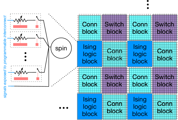
There are at least four points of departure for FPIMs compared to traditional FPGA architectures. First, our results (see Sec. IV) show a slightly higher connectivity requirement compared to traditional FPGAs, which can be compensated for by increasing the number of routing tracks. Second, connectivity requirements for coupling resistors are bi-directional, which requires pass-transistor based configuration rather than the direct drive architectures seen in modern FPGAs. Third, much larger pass transistors will be needed to ensure that coupling resistance values are primarily determined by programmable resistors rather than the interconnect. Fourth, a suitable choice of logic block I/O connectivity must be selected for the local island in the island-style architecture.
An example overall architecture with one spin per logic block is shown in Fig. 4. Note that this is a logical diagram, not a physical one because the wires will be partially routed over the Ising logic block. The connection box and switch box will contain programmable cross-points implemented with large pass transistors to reduce the resistance of the programmable interconnect relative to the explicit coupling resistors required. Switch boxes permit programmable connectivity between horizontal and vertical routing tracks, while connection boxes provide connectivity between the Ising logic block and the interconnect tracks. We can use pass-transistors to build switches that have negligible additive resistance values compared to the desired coupling values. We also observe that the bi-directional nature of coupling in FPIM implies that the FPGA architecture and interconnect problem for FPIM is not exactly the same as that in traditional synchronous FPGAs, where the switch boxes can be used to split and fanout digital signals to multiple end-points without any loss/impact on correct operation. However, the routing problem is similar to the point-to-point pipelined interconnect required in high-throughput asynchronous FPGAs [24].
Finally, if a spin has extremely high connectivity, we can introduce mirror spins and force these spins to match each other. This permits decomposition of the small number of spins that have large connectivity for embedding into the FPIM architecture.
In a traditional FPGA architecture, the programmable routing fabric dominates the area, delay, and energy of the FPGA. While we will show that the area overhead of routing is slightly lower than a traditional FPGA for FPIMs, the energy and delay metrics for FPIMs are quite different. In particular, the goal of the programmable routing is to resistively couple slow, time-varying, analog voltages to each other, rather than transmitting a digital signal transition. The programmable resistors that are part of the logic block are designed to have significantly higher resistance values (20 or more) than the pass transistor logic for the interconnect, permitting us to treat the interconnect resistance as negligible. Hence, the performance and power consumption of the entire system will be dominated by the non-linear dynamics of the spin-coupled analog Ising hardware i.e., an FPIM will be logic-block dominated, unlike FPGAs that are interconnect dominated. The key question to answer is: can we design an interconnect that is routable, i.e., supports a wide range of Ising-mapped SAT problems? We focus on this in the evaluation next.
IV FPIM metrics on SAT benchmarks
We mapped two sets of SAT problems, uf20 and uf50 from DIMACS SATLIB [19] (each consisting of 1000 problems), into Ising form using the above techniques. uf20 problems each have 20 variables and 91 clauses, while uf50 problems feature 50 variables and 218 clauses. Employing yosys/ABC, we synthesized each problem using three different technology libraries: 1) the 2inp set of logic gates shown in Table 1, 2) NAND gates only, and 3) OR and NOT gates only.131313Being logically complete, NAND and OR-NOT are capable of synthesizing any SAT problem. Note that all the Ising equivalent weights for gates in the 2inp library are between -2 and +2, which bodes well for the BCR of our Ising formulation of SAT.
The Ising equivalent network is generated from the SATLIB problem (in .cnf format) via automated custom tools we have written. These tools perform gate-level synthesis using yosys and ABC, calculate Ising equivalents for the gates needed (e.g., like those in Table 1) and use them to translate the gate-level netlist into an Ising-equivalent one.
To assess hardware requirements for FPIMs, we study the characteristics of the Ising formulation of SAT problems that directly impact hardware resource requirements for a programmable architecture. In particular, we looked at the distributions of the number of spins needed, the sparsity of connections (degree of each spin node), and the BCR needed to program each weight value. The distributions over the 1000 problems in each set are shown in Tables 2 to 4. Each table shows distributions for the three technology mappings used.
It can be seen in Table 2 that over the 1000 problems in the uf20 benchmark set, the majority (more than 900) require between 151 and 200 spins if the 2inp technology library is applied.141414The numbers in parentheses in Table 2 are for a modified mapping, explained below. However, if the NAND-only and OR-NOT-only libraries are used, the range shifts to 251-300 and 301-350, respectively. The sparsities (average number of nodes each node is connected) over all the uf20 problems are shown in Table 3. The table reveals that all three technology mappings have roughly the same sparsity characteristics, with the majority of nodes having between 1 and 5 connections. The BCR distribution, i.e., the count of connections that need a given number of bits to program their weight values, is shown in Table 4. It can be seen that 3 bits of coupling resolution suffice for the majority of connections over all the problems, with a smaller number of 4 and 5 bit connections also needed; and that these requirements are largely independent of the technology mapping used. This constitutes important information for planning and designing an FPIM for uf20 problems.
| lib | 2inp | NAND | N/OR | 2inp | NAND | N/OR |
| # spins | uf20 | uf50 | ||||
| 0-150 | 1 (0) | |||||
| 151-200 | 760 (346) | |||||
| 201-250 | 239 (654) | 61 | ||||
| 251-300 | 0 (29) | 845 | 76 | |||
| 301-350 | 94 | 862 | ||||
| 351-400 | 62 | |||||
| 500-600 | 922 (557) | |||||
| 601-701 | 78 (443) | |||||
| 701-801 | 27 | |||||
| 801-901 | 783 | 411 | ||||
| 901-1000 | 190 | 589 | ||||
Similar data on the 1000 uf50 problems is shown in the latter columns of Tables 2, 3 and 4. Since these have more Boolean variables than uf20, it is not surprising that larger numbers of spins are required in their Ising mappings. Like for uf20, the 2inp library results in significantly more compact mappings from a number-of-spins perspective, with every problem mapped using between 601 and 800 spins. We determined empirically that the number of Ising spins grows as () with respect to the number of SAT variables . Note, however, that the sparsity (Table 3) and BCR (Table 4) distributions are very similar to those of uf20. This provides the important insight that while the number of spins increases as SAT problem sizes increase, the number of connections each spin requires, as well as the number of bits required to program those connections, remains roughly the same. This directly implies that scalable FPIM architectures for arbitrary SAT-to-Ising problem sizes are possible without having to scale up connectivity and BCR requirements with problem size.
| lib | 2inp | NAND | NOT/OR | 2inp | NAND | NOT/OR |
|---|---|---|---|---|---|---|
| degree | uf20 | uf50 | ||||
| 1-5 | 160.1 | 225.9 | 225.9 | 501.4 | 749.6 | 783.7 |
| 6-10 | 12.6 | 36.4 | 36.7 | 22.3 | 60.6 | 60.8 |
| 11-20 | 16.3 | 14.1 | 14.2 | 23.3 | 58.4 | 58.5 |
| 21-31 | 2.5 | 0.01 | 0.013 | 25.3 | 3.489 | 1.124 |
| 32-41 | 0.817 | |||||
| lib | 2inp | NAND | NOT/OR | 2inp | NAND | NOT/OR |
|---|---|---|---|---|---|---|
| BCR | uf20 | uf50 | ||||
| 1 | 223.4 | 319.3 | 476.4 | 745.3 | 1056 | 1375.0 |
| 2 | 357.0 | 409.0 | 457.9 | 1070.5 | 1300.6 | 1326.9 |
| 3 | 110.6 | 133.0 | 20.0 | 287.01 | 318.3 | 32.645 |
| 4 | 0.798 | 14.2 | 14.1 | 4.301 | 56.015 | 56.074 |
| 5 | 0.001 | 0.085 | 0.087 | 0.06 | 3.489 | 3.535 |
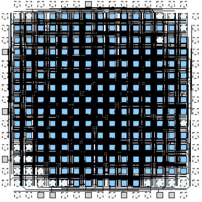
To determine the interconnect complexity required for an FPIM, we used the open-source VPR FPGA place-and-route software package [25]. We created an FPGA architecture description file for VPR that treats each spin as a place-able component. Connectivity is determined by the Ising problem generated via our SAT-to-Ising automated mapping flow. The interconnect has half-populated connection blocks, with a standard Wilton-style switch block, with direct connections to resistors connected to spins. The routing tracks are all singles (i.e., single-hop per switch point). We ran the uf20 and uf50 problems through place-and-route to determine the number of routing tracks necessary to support each problem. Fig. 5 shows an example uf20 problem placed and routed on an FPIM. All the uf20 benchmarks can be mapped to an FPIM with less than 20 routing tracks, and all the uf50 benchmarks can be mapped to an FPIM with less than 36 routing tracks. While these numbers are slightly higher than conventional FPGAs given the problem size, they are well within the capabilities of a modern CMOS process.
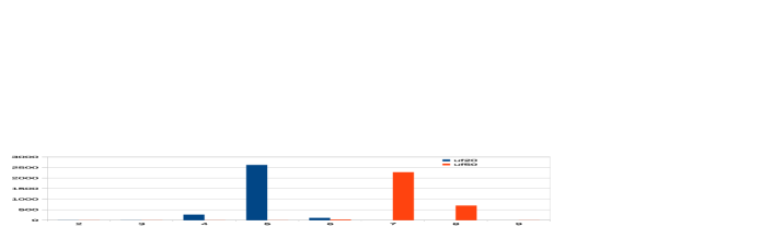
To reduce the interconnect requirements at the cost of slightly increased spins, we incorporated a spin mirror step after the Ising problems were created. The spin mirror step examines spins that have high connectivity (more than 8), and introduces a replica spin to reduce the connectivity in the Ising formulation where the replica is generated by inserting a buffer gate prior to Ising mapping. The numbers in parentheses in Table 2 show the increase in spins as a result of this transformation. This is similar to the process of buffer insertion in digital logic to reduce delay, but our motivation is to reduce the complexity of the programmable interconnect. We re-ran VPR on the 6,000 benchmarks (2,000 problems, 3 libraries per problem). We found that all the uf20 benchmarks were routable with 6 tracks for a 6.3% increase in number of spins, and all the uf50 benchmarks were routable with 9 tracks for a 3.9% increase in number spins a 3.3-4 reduction in the number of routing tracks. Fig. 6 shows the histogram of routing track requirements across all libraries and benchmarks (3,000 scenarios for uf20 and for uf50).
Using the above information, we have estimated the areas of all the components needed to make an FPIM, including analog spin circuits,151515assuming ring oscillators, which require more devices than, e.g., CMOS latches. programmable resistors implemented using transmission gate ladders, and transmission gate based switch boxes, connection boxes and input MUXes. The overall estimate came to about 10M per spin, where represents half of the technology’s feature size. Unlike in FPGAs, this area is strongly dominated by the analog components, i.e., the analog spins and programmable coupling resistors. In a 65nm process, for example, a 1000-spin FPIM, which is more than adequate for all the uf50 and uf20 problems, would occupy about 10mm2. This shows that FPIMs are in fact a practical way to implement configurable IM solvers.
Conclusion
Specializing analog Ising solver ICs for problem classes is likely a more practically feasible and competitive approach than re-mapping onto fixed, regular Ising connection topologies. We have shown that SAT problems can be mapped onto a novel but very realistic reconfigurable analog Ising solver architecture, FPIM. We have assessed feasibility using key metrics: the number of spins needed, connection sparsity, and the number of bits needed to program connection weights (BCR). FPIM is not limited to a specific electronic spin circuit, but can employ spin circuits from several available analog Ising schemes. A 1000-spin FPIM, which suffices for all 2000 SAT benchmark problems we considered, would occupy about mm2 in a 65nm process. FPIM is a significant step towards practical analog Ising solver ICs for SAT and possibly other CO problems.
References
- [1] M. W. Johnson et al., “Quantum annealing with manufactured spins,” Nature, vol. 473, no. 7346, pp. 194–198, 2011.
- [2] Z. Wang et al., “Coherent Ising machine based on degenerate optical parametric oscillators,” Phys. Rev. A, vol. 88, no. 6, 2013.
- [3] T. Wang, L. Wu, P. Nobel, and J. Roychowdhury, “Solving combinatorial optimisation problems using oscillator based Ising machines,” Natural Computing, pp. 1–20, April 2021.
- [4] R. Afoakwa et al., “BRIM: Bistable Resistively-Coupled Ising Machine,” in IEEE HPCA, 2021, pp. 749–760.
- [5] J. Roychowdhury, “Bistable Latch Ising Machines,” Proc. UCNC, October 2021.
- [6] I. Ahmed et al., “A Probabilistic Compute Fabric Based on Coupled Ring Oscillators for Solving Combinatorial Optimization Problems,” IEEE J. Solid-State Ckts., vol. 56, no. 9, September 2021.
- [7] K. Tatsumura, M. Yamasaki, and H. Goto, “Scaling out Ising machines using a multi-chip architecture for simulated bifurcation,” Nature Electronics, vol. 4, no. 3, pp. 208–217, 2021.
- [8] K. Tatsumura, A. R. Dixon, and H. Goto, “FPGA-based simulated bifurcation machine,” in Proc. FPL, 2019, pp. 59–66.
- [9] A. Lucas, “Ising formulations of many NP problems,” Frontiers in Physics, vol. 2, p. 5, 2014.
- [10] M. Kim et al., “Leveraging quantum annealing for large MIMO processing in centralized radio access networks,” in Proc. ACM SIG on Data Comm., 2019.
- [11] J. Roychowdhury, J. Wabnig and K.P. Srinath, “Performance of Oscillator Ising Machines on Realistic MU-MIMO Decoding Problems,” Web link to preprint.
- [12] N. Sagan and J. Roychowdhury, “DaS: Implementing Dense Ising Machines Using Sparse Resistive Networks,” in Proc. ICCAD, November 2022.
- [13] K. Boothby et al., “Next-Generation Topology of D-Wave Quantum Processors,” arXiv:2003.00133, 2020.
- [14] J. Su, T. Tu, and L. He, “A quantum annealing approach for Boolean Satisfiability problem,” in Proc. IEEE DAC, 2016.
- [15] Y. Sugie et al., “Minor-embedding heuristics for large-scale annealing processors with sparse hardware graphs of up to 102,400 nodes,” Soft Comput., vol. 25, no. 3, 2021.
- [16] T. Wang, L. Wu and J. Roychowdhury, “New Computational Results and Hardware Prototypes for Oscillator-based Ising Machines,” in Proc. IEEE DAC, 2019, pp. 239:1–239:2.
- [17] C. Wolf, J. Glaser, and J. Kepler, “Yosys—a free Verilog synthesis suite,” in Proc. Austrochip, 2013.
- [18] R.K. Brayton and A. Mishchenko, “ABC: An Academic Industrial-Strength Verification Tool,” in Proc. CAV, 2010.
- [19] H. H. Hoos and T. Stützle, “SATLIB: An online resource for research on SAT,” SAT, vol. 2000, pp. 283–292, 2000.
- [20] R. M. Karp, “Reducibility among combinatorial problems,” in Complexity of Computer Computations. Springer, 1972, pp. 85–103.
- [21] L. Zhang and S. Malik, “The Quest for Efficient Boolean Satisfiability Solvers,” in International Conference on Computer Aided Verification, 2002, pp. 17–36.
- [22] J. Marques-Silva, “Practical applications of Boolean Satisfiability,” in 9th Int. Workshop on Discrete Event Syst., 2008.
- [23] Z. Bian, F. A. Chudak, W. G. Macready, A. Roy, R. Sebastiani, and S. Varotti, “Solving SAT and MaxSAT with a Quantum Annealer: Foundations, Encodings, and Preliminary Results,” arXiv:1811.02524, November 2018.
- [24] J. Teifel and R. Manohar, “Highly pipelined asynchronous FPGAs,” in Proc. FPGA, 2004, pp. 133–142.
- [25] V. Betz and J. Rose, “VPR: A new packing, placement and routing tool for FPGA research,” in Proc. FPL, 1997, pp. 213–222.