Dynamic enhancement of conductance in fractional quantum Hall constriction
Sampurna Karmakar, Amulya Ratnakar and Sourin Das
Department of Physical Sciences
Indian Institute of Science Education and Research (IISER) Kolkata
Mohanpur - 741246,
West Bengal, India
Abstract
AC transformer action of a quantum point contact separating quantum Hall states with distinct filling fractions is studied theoretically. The AC gain () of this setup is shown to exceed its DC bound () for a certain range of frequency in the presence of appropriate inter-electron interactions owing to displacement current induced by the ambient gate electrodes. This setup is also endowed with the unique possibility of having frequency tunable resonances and anti-resonances across the QPC.
Proximity-induced superconducting correlation locally at the edge of a quantum Hall (QH) state could open up a possibility for the design of an almost dissipation-free mesoscopic DC voltage transformer owing to its topological immunity from backscattering. The transformer action can be understood from the fact that a positive input voltage imposed on the edge flowing into a region, where the edge is strongly coupled to a superconductor (SC), would result in a negative output voltage on the edge flowing out of that region due to Andreev processAndreev (1964). Such junction between QH edge and SC has been experimentally realized recently not only for integer filling fractionSahu et al. (2018); Lee et al. (2017); Rickhaus et al. (2012); Jeong et al. (2011); Mizuno et al. (2013); Efetov et al. (2016); Amet et al. (2016); Hatefipour et al. (2022) but also for fractional fillingsGül et al. (2022). But this is expected to be a difficult route as stabilizing superconductivity at large magnetic fields is difficult. Alternatively, a similar transformer action, pointed out by Chklovskii and HalperinChklovskii and Halperin (1998), can also be induced by employing a junction, a quantum point contact (QPC) between two QH states such that the quasi-particle charge on the two sides of the junction is different, leading to Andreev-like process Sandler et al. (1998). Such an Andreev-like process was first noted by Safi and Schulz in the context of non-chiral Luttinger liquid (LL)Safi and Schulz (1995). A simple-minded description of this physics for the case of and 1/3 state can be understood as follows. An incident excited quasi-particle of charge on the edge can tunnel across the junction only if it pairs up with two more quasi-particles at the junction, hence forming an electron. The tunneling process will result in two holes reflecting on the edge, similar to an Andreev reflected hole at a normal metal-superconductor junction. Consequently, such an Andreev process in the absence of superconductivity can be harvested for dissipation-less transformer action.
Such setups based on two-dimensional electron gas (2DEG) platforms with the extended junction between has been reported Cohen et al. (2019); Maiti et al. (2020); Ronen et al. (2018). A finite but not perfect Andreev reflection (accompanied by normal reflection) from a QPC between junction has also been experimentally observed in 2DEG Hashisaka et al. (2021). More recently, a graphene-based QPC linking and QH edge states have been realized experimentally Cohen et al. (2022) and a perfect Andreev reflection limit has been achieved, paving the way for a nearly dissipationless DC voltage
step-up transformer with a gain of .
All the previous theoretical and experimental studies in this context primarily focused on the DC limit, which is blind to the capacitive coupling to the ambient gated environment. Hence, AC response is expected to open up new avenues both in terms of its physics and practical application of such junctions.
An AC study comprises two complementary approaches: (a) frequency domain analysis Safi and Schulz (1995); Safi (1999); Hashisaka et al. (2012); Washio et al. (2011); Degiovanni et al. (2010); Müller et al. (2017); Agarwal (2014); Soori and Sen (2011); Hashisaka and Fujisawa (2018) and (b) time domain analysisSafi and Schulz (1995); Calzona et al. (2015); Soori and Sen (2011); Agarwal (2014); Hashisaka and Fujisawa (2018); Kamata et al. (2014). We show that, in the presence of generalized interedge interactions, motivated by bilayer stacking geometry Boebinger et al. (1990); Suen et al. (1991); Eisenstein et al. (1992); Manoharan et al. (1997); Li et al. (2018); Overweg et al. (2018) (see fig. 1), there exist, frequency bands, over which the AC conductance exceeds the DC bound of . This enhancement in gain beyond the DC limit is shown to be related to the displacement current. Also, there are magic frequencies at which reflectance vanishes, and the gain hits the maximum value of for junction. The parameter space of interaction, over which these bands of excess gain appear in the frequency domain, always shows distinctive behavior in the time evolution of electron wave-packet in terms of hole pulses in the transmitted edge channel, which otherwise is absent.
One of the peculiarities of AC conductance calculation for mesoscopic setup is the violation of Kirchhoff’s law. This apparent current non-conservation was addressed for the non-interacting mesoscopic system by Büttiker et. al. Prêtre et al. (1996); Büttiker (1990); Büttiker et al. (1993) and later by Safi in the context of LLs Safi (1999). In what follows, we will closely comply with the plasmon scattering approach developed by Safi Safi (1997, 1999) for the AC conductivity matrix for such a system.
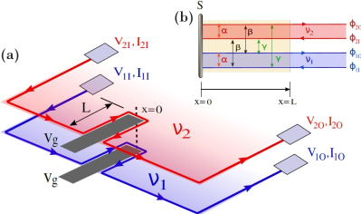
Figure 1: (a) Shows stacking of bilayer QH states with filling fractions and with QH edges being manipulated using a gate electrode with potential . The two edge states in the two FQH layers are locally tunnel coupled at . () stands for current (voltage) on the incoming/ outgoing channels. In (b), denotes the bosonic field corresponding to the incoming/outgoing edge state of the QH layer. denote the density-density repulsive interactions between the QH layers. The boundary condition at is denoted through the current splitting matrix .
Junction of Interacting Quantum Hall Edge States: Consider a junction of edge states realized at the boundary of two fractional QH (FQH) systems with filling fractions and in a bilayer stackingRatnakar and Das (2021). We use the folded basis to describe the FQH edge junction such that all the QH edge states lie between and , with the tunnel junction positioned at . The edge states in the two FQH states can be brought closer to each other in a finite region , using gate electrodes, to allow for interedge interactions. The two quantum wells hosting distinct FQH states can be engineered in a way that, after the distance ‘’ from the junction, the edge states of the two FQH systems move away from each other (see fig. 1). As a result, the density-density interaction between the edge states gets quenched beyond .
We describe the low-energy physics of the FQH edge junction setup using the bosonization technique and formulate the AC conductivity matrix using the plasmon scattering matrix approach. In the standard bosonization formula, it is possible to express the fermionic field associated with the electron situated on the edge in terms of the bosonic fields Haldane (1981); von Delft and Schoeller (1998); Maslov (2005); Wen (1990a, b, 1991) as , where are the corresponding Klein factors, denotes filling fraction and the subscript describes an incoming (outgoing) bosonic field at the junction. Then, the Lagrangian density for the interacting edge, in the bosonized form, is given by
Here, denotes the Fermi velocity, and the matrix is given by
(1)
The density-density interactions are denoted as:
(1) is the interaction between the counter-propagating edge states in the same QH layer (intralayer interaction).
(2) is the interaction between the co-propagating edge states of different QH layers (interlayer interaction).
(3) is the interaction between the counter-propagating edge states of different QH layers (interlayer interaction).
Using Eq. Dynamic enhancement of conductance in fractional quantum Hall constriction, one can diagonalize the Hamiltonian and get the Heisenberg equation of
motion Das et al. (2009); Ratnakar and Das (2021), and also formulate a plasmon scattering matrix, relating the oscillator modes of the incoming bosonic field to the outgoing bosonic field in the free region, by matching the fields at in accordance to the equation of motion (see supplemental material). The boundary condition (BC) at the tunneling point, , is also accounted for in the formalism. The BC is determined by the current conserving splitting matrix at the junction, which may be represented by the fixed point, such that . The renormalized velocities are, and .
The AC scattering matrix , relating the oscillator modes of the incoming physical fields ( for ) to the outgoing physical modes ( for ) in the non-interacting region (), is given by
(2)
There are only two allowed junction fixed points for such a setup considered here, leading to two possible current splitting matrices ,
(3)
where the fully reflecting disconnected fixed point and the strongly coupled fixed point are denoted by and Wen (1994); Sen and Agarwal (2008); Sandler et al. (1998) respectively.
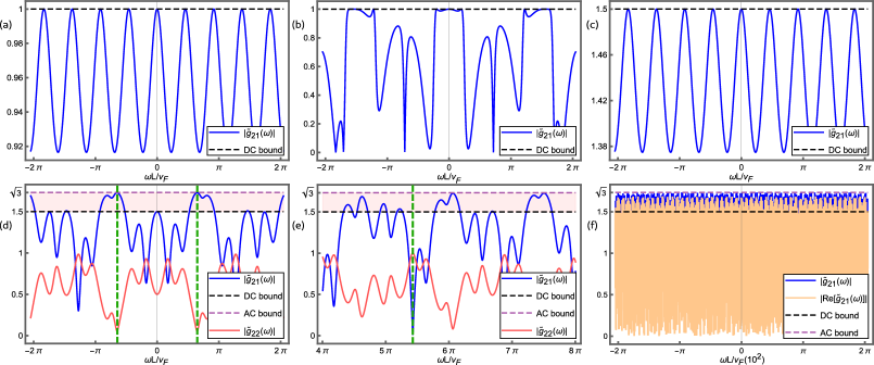
Figure 2: is plotted as a function of frequency for an injection from side. is plotted (with ) for the case when (a) and (b) , (c) . (d) and (e) shows and for along with the resonance and anti-resonance points for respectively (denoted by vertical green dashed lines). (f) shows along with in the large limit ( is taken to be 100). DC and AC bounds are shown by dashed black and purple lines, respectively.
The chiral AC conductivity matrix, , then can be written as Maslov (1995)
(4)
where, an electron initially emanates at and finally reaches . The conductance matrix relates the local incoming edge potential at to the outgoing edge current at , such that, , where and . In the DC limit, that is, , the AC scattering matrix reduces to the corresponding junction fixed point matrix S (see Eq. 3) at , such that the DC conductivity matrix is given by
(5)
and indicates the fact that the DC conductivity is insensitive to the density-density interactions (see Eq. 1) present in the system.
Outgoing electron current at is related to incoming electron current at through the relation, , where has the form
(6)
and denotes the total dynamic transmission (reflection) coefficient for the incident current from the incoming edge to the (into the ) outgoing edge. At the boundary of the interacting region (),
(7)
It is important to note that with and , indicating the apparent violation of the current conservation condition.
Total charge conservation is restored by accounting for displacement currents, which may get induced in the capacitively coupled conductors (such as confining potential gates, QPC gates, etc.) Safi (1999); Büttiker et al. (1993); Prêtre et al. (1996); Büttiker (1990). Assuming a one-dimensional model for capacitively coupled conductors, the net local induced current is taken to be the difference of the net local incoming current and a net local outgoing current . Now, an AC current splitting matrix, , obeying the current conservation condition and relating the incoming and outgoing currents, can be defined as
. is given by and is given by . An AC current conservation imposes the condition . Then, a chiral AC conductance matrix, can be formed relating the local outgoing current, , to the local incoming edge potential, (see supplemental material), where .
For a FQH edge junction of and , tuned to strong coupling fixed point (SCFP), the total current conserving conductivity matrix, is given by
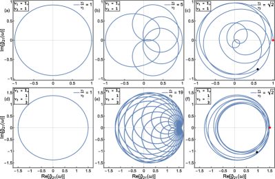
Figure 3: vs is plotted as a function of frequency () for different and for (top row) and (bottom row) junction. (a) and (d) are plotted for , (), (b) is for (), (e) is for (), (c) and (f) are for (). The red and black dots indicate the initial and final frequency of the trajectory, respectively.
where .
Eq. 9 implies that for , . The maximum value that and can take is and 1, respectively, for any set of interaction parameters . Note that . A voltage conversion matrix with the components being can be defined as
(10)
where and with . For an injection from side with , the AC gain , which is quantity of central interest is defined asCohen et al. (2022)
(11)
with being grounded and it is maximized to the value of . For , = . Note that at these resonant frequencies, attains maximum value, while both and are simultaneously zero. A reverse scenario is also possible for certain frequencies for which both and are simultaneously zero, while attains the maximum value of one.
For a junction of , does not attain a value beyond 1 (see fig. 2(a, b)). A junction of and QH edge states, which already shows an enhanced transmitted current in the DC limit , in the presence of only intra-layer interaction (), the AC current amplitude does not go beyond its DC limit, i.e., (as shown in fig. 2(c)). However, in the presence of inter-layer interaction (), when the current is excited along the incoming edge, the transmitted current amplitude may even go beyond its DC limit, resulting in a maximum gain, , at resonant frequencies (see fig. 2(d)). The excess current beyond unit amplitude is compensated by the displacement current in the capacitive coupled ambient gate. Hence, this provides a basic setup to realize a step-up AC transformer with higher efficiency as compared to its DC counterpart in a QPC geometry. Also, in the large ’ limit, in the finite frequency regime, the gain is almost always larger than the DC bound of and both the real and imaginary part of contributes significantly(see fig. 2(f) for the real part).
Now we study the non-trivial dependence of conductance on frequency. In fig. 3, a parametric plot of , is presented as function of frequency () for different ratios. Note that for the case when and and there is only one timescale corresponding to the time of flight of plasmons in the cavity and hence vs is a simple close loop (see fig. 3(a, d)) for both and . For , we have taken for simplicity. For any integer (or rational) the conductance is periodic function of (see fig. 3(b, e)) and interestingly it depicts transmission zeros (anti- resonances). However, for irrational ratios of (see fig. 3(c, f)), we note that the loop does not close onto itself, hence indicating that there is no periodicity of the system in the frequency domain.
The above conductances can also be obtained via a wave packet dynamics approach Safi and Schulz (1995); Calzona et al. (2015); Soori and Sen (2011); Agarwal (2014); Hashisaka and Fujisawa (2018); Kamata et al. (2014) in the time domain (see supplemental material). Interestingly, we note that in response to an injected wave packet, a distinct nature of fractionalized negative pulses in the transmitted edge channel appears, which is specific to the presence of interlayer interaction. The results presented in this letter are significant in light of recent experiments where a QPC geometry and an extended long junction geometry on a two-dimensional electronic systems Maiti et al. (2020); Ronen et al. (2018); Hashisaka et al. (2021); Cohen et al. (2022) are realized. Here, we present a study of SCFP in the AC regime and show that an appropriate set-up design could open up a new avenue in terms of potential applications in quantum-inspired technologies such as step-up transformers with amplification beyond the experimentally observed DC limit and give rise to resonances and anti-resonances in transmitted current at magic frequencies, which we can make use of as frequency filters. Furthermore, for rational ratios of and , the periodic nature of the conductance as a function of frequency in the complex plane is studied in fig. 3, which has been discussed experimentally in Ref.[ Bocquillon et al. (2013)]. We also note that a realistic model of QPC-induced interaction region of length of few m Bocquillon et al. (2013); Inoue et al. (2014); Bäuerle et al. (2018); Kataoka et al. (2016); Freulon et al. (2015) with the parameter space of interaction strength that we are working with, the estimated range for resonance frequency can be of the order of 1-15 GHz for typical propagation velocity of m/s Bäuerle et al. (2018); Freulon et al. (2015); Kataoka et al. (2016); Ryu and Sim (2022) for the plasmon which is well within experimental reach[ Bocquillon et al. (2013)].
Acknowledgements:
The authors would like to thank Biswajit Karmakar and Suvankar Purkait for their useful discussion regarding AC transport in QH circuits. A.R. acknowledges the University Grants Commission, India, for support through fellowship. S.K. is thankful to the Ministry of Education of the Government of India for financial support through the Prime Minister’s Research Fellows (PMRF) grant.
Lee et al. (2017)
G.-H. Lee, K.-F. Huang, D. K. Efetov, D. S. Wei, S. Hart, T. Taniguchi, K. Watanabe, A. Yacoby, and P. Kim, Nature Physics 13, 693 (2017), ISSN 1745-2481, URL https://doi.org/10.1038/nphys4084.
Rickhaus et al. (2012)
P. Rickhaus, M. Weiss, L. Marot, and C. Schönenberger, Nano Letters 12, 1942 (2012), ISSN 1530-6984, URL https://doi.org/10.1021/nl204415s.
Mizuno et al. (2013)
N. Mizuno, B. Nielsen, and X. Du, Nature Communications 4, 2716 (2013), ISSN 2041-1723, URL https://doi.org/10.1038/ncomms3716.
Efetov et al. (2016)
D. K. Efetov, L. Wang, C. Handschin, K. B. Efetov, J. Shuang, R. Cava, T. Taniguchi, K. Watanabe, J. Hone, C. R. Dean, et al., Nature Physics 12, 328 (2016), ISSN 1745-2481, URL https://doi.org/10.1038/nphys3583.
Amet et al. (2016)
F. Amet, C. T. Ke, I. V. Borzenets, J. Wang, K. Watanabe, T. Taniguchi, R. S. Deacon, M. Yamamoto, Y. Bomze, S. Tarucha, et al., Science 352, 966 (2016), eprint https://www.science.org/doi/pdf/10.1126/science.aad6203, URL https://www.science.org/doi/abs/10.1126/science.aad6203.
Hatefipour et al. (2022)
M. Hatefipour, J. J. Cuozzo, J. Kanter, W. M. Strickland, C. R. Allemang, T.-M. Lu, E. Rossi, and J. Shabani, Nano Letters 22, 6173 (2022), ISSN 1530-6984, URL https://doi.org/10.1021/acs.nanolett.2c01413.
Gül et al. (2022)
O. Gül, Y. Ronen, S. Y. Lee, H. Shapourian, J. Zauberman, Y. H. Lee, K. Watanabe, T. Taniguchi, A. Vishwanath, A. Yacoby, et al., Phys. Rev. X 12, 021057 (2022), URL https://link.aps.org/doi/10.1103/PhysRevX.12.021057.
Cohen et al. (2019)
Y. Cohen, Y. Ronen, W. Yang, D. Banitt, J. Park, M. Heiblum, A. D. Mirlin, Y. Gefen, and V. Umansky, Nature Communications 10, 1920 (2019), ISSN 2041-1723, URL https://doi.org/10.1038/s41467-019-09920-5.
Ronen et al. (2018)
Y. Ronen, Y. Cohen, D. Banitt, M. Heiblum, and V. Umansky, Nature Physics 14, 411 (2018), ISSN 1745-2481, URL https://doi.org/10.1038/s41567-017-0035-2.
Hashisaka et al. (2021)
M. Hashisaka, T. Jonckheere, T. Akiho, S. Sasaki, J. Rech, T. Martin, and K. Muraki, Nature Communications 12, 2794 (2021), ISSN 2041-1723, URL https://doi.org/10.1038/s41467-021-23160-6.
Cohen et al. (2022)
L. A. Cohen, N. L. Samuelson, T. Wang, T. Taniguchi, K. Watanabe, M. P. Zaletel, and A. F. Young, Universal chiral luttinger liquid behavior in a graphene fractional quantum hall point contact (2022), eprint 2212.01374, URL https://doi.org/10.48550/arXiv.2212.01374.
Safi (1999)
I. Safi, The European Physical Journal B - Condensed Matter and Complex Systems 12, 451 (1999), ISSN 1434-6036, URL https://doi.org/10.1007/s100510051026.
Washio et al. (2011)
K. Washio, M. Hashisaka, H. Kamata, K. Muraki, and T. Fujisawa, Japanese Journal of Applied Physics 50, 04DJ04 (2011), URL https://dx.doi.org/10.1143/JJAP.50.04DJ04.
Kamata et al. (2014)
H. Kamata, N. Kumada, M. Hashisaka, K. Muraki, and T. Fujisawa, Nature Nanotechnology 9, 177 (2014), ISSN 1748-3395, URL https://doi.org/10.1038/nnano.2013.312.
Overweg et al. (2018)
H. Overweg, H. Eggimann, X. Chen, S. Slizovskiy, M. Eich, R. Pisoni, Y. Lee, P. Rickhaus, K. Watanabe, T. Taniguchi, et al., Nano Letters 18, 553 (2018), ISSN 1530-6984, URL https://doi.org/10.1021/acs.nanolett.7b04666.
Maslov (2005)
D. L. Maslov, Fundamental aspects of electron correlations and quantum transport in one-dimensional systems (2005), eprint cond-mat/0506035, URL https://doi.org/10.48550/arXiv.cond-mat/0506035.
Bocquillon et al. (2013)
E. Bocquillon, V. Freulon, J.-. M. Berroir, P. Degiovanni, B. Plaçais, A. Cavanna, Y. Jin, and G. Fève, Nature Communications 4, 1839 (2013), ISSN 2041-1723, URL https://doi.org/10.1038/ncomms2788.
Bäuerle et al. (2018)
C. Bäuerle, D. C. Glattli, T. Meunier, F. Portier, P. Roche, P. Roulleau, S. Takada, and X. Waintal, Reports on Progress in Physics 81, 056503 (2018), URL https://dx.doi.org/10.1088/1361-6633/aaa98a.
Kataoka et al. (2016)
M. Kataoka, N. Johnson, C. Emary, P. See, J. P. Griffiths, G. A. C. Jones, I. Farrer, D. A. Ritchie, M. Pepper, and T. J. B. M. Janssen, Phys. Rev. Lett. 116, 126803 (2016), URL https://link.aps.org/doi/10.1103/PhysRevLett.116.126803.
Freulon et al. (2015)
V. Freulon, A. Marguerite, J.-M. Berroir, B. Plaçais, A. Cavanna, Y. Jin, and G. Fève, Nature Communications 6, 6854 (2015), ISSN 2041-1723, URL https://doi.org/10.1038/ncomms7854.
Supplemental material for “Dynamic enhancement of conductance in fractional quantum Hall constriction"
Sampurna Karmakar, Amulya Ratnakar and Sourin Das
Department of Physical Sciences
Indian Institute of Science Education and Research (IISER) Kolkata
Mohanpur - 741246,
West Bengal, India
I Calculation for AC conductance matrix
Consider fig. 1 of the main text. The interacting edge Hamiltonian describing our setup, in bosonized form, is given by
(I.1)
where the kinetic and the interacting part of the total Hamiltonian (H) is given by , and the coupling to the ambient gates is accounted by .
(I.2)
where the incoming/outgoing electronic density, for , is the Fermi velocity, and the matrix is given by
We will closely comply with the plasmon scattering approach developed by I. Safi Safi (1999) for the calculation of the AC conductivity matrix of our system.
A gauge transformation of the chiral fermionic fields yields a substitution for the chiral bosonic fields and the corresponding densities as
(I.3)
(I.4)
and the presence of a vector potential ‘’ modifies the Hamiltonian as
(I.5)
From here, the current field can be expressed for the Hamiltonian as
(I.6)
Hence, takes the form
(I.7)
where, is the local chemical potential and the local potential is given by .
Using these relations, one can formulate the AC current splitting matrix relating all the incoming currents at a point to the outgoing currents at the same point as
(I.8)
where denotes the total dynamic transmission(reflection) coefficient for the incident current from the incoming edge to the outgoing edge (into the outgoing edge). The requirement of AC current conservation imposes the condition that the columns of the matrix should add up to 1, i.e.
(I.9)
Again, the relation between voltages and currents on the edges is, . Hence,
(I.10)
where the elements of the matrix are given by the filling fraction of the two QH bulk and the ambient gates, such that .
If all the edges have the same input bias voltage, each row of the matrix should add up to 1, such that the voltages at the outgoing edges are also the same.
(I.11)
Now, the conductance matrix calculated at the interaction region boundary, , is given by as
, which is the part of the conductance matrix , can be calculated using the plasmon scattering matrix approach Safi and Schulz (1995); Das et al. (2009); Ratnakar and Das (2021).
The Lagrangian density, , only for the interacting edges, in the bosonized form, is given by
(I.14)
Here, for , for and is the matrix accounting for coordinate dependent inter-edge interaction. The commutation relation between the physical bosonic fields is given by . One can get the equation of motions from eq. I.14 as
,
,
,
.
(I.15)
The boundary condition (BC) at can be obtained by integrating Eq. I.15 over the coordinate from to in the limit . The BC at is determined by the current conserving splitting matrix at the junction, such that . In the non-interacting region, , the physical bosonic field is given by the chiral mode expansion:
(I.16)
where, () is the bosonic annihilation (creation) operator, such that . The commutation relation for the physical fields is given by .
In the interacting region, that is , the physical fields can be expressed as the linear combination of Bogoliubov (Bg) fields, , such that
(I.17)
where, , and . The bosonic mode expansion for the chiral Bg modes in the interacting region is given by
(I.18)
where () is the bosonic annihilation (creation) operator, such that . is the renormalized velocity and . The commutation relation for Bg fields is given by . Taking into account the BC at and the fact that the physical fields follow the equation of motion in the interacting region, the physical bosonic field can be expressed in terms of Bg fields at finite distance ‘’ () from the junction as,
(I.19)
where, and
(I.20)
where, matrix .
The inter-electron interaction between the FQH edge states renormalizes the Fermi velocity, such that and . Since the system is non-dissipative, we impose the condition, and that the current spitting matrix at the junction is given by the current conserving fixed point of the theory.
The continuity of bosonic fields at ensures that the current is conserved across the interacting region boundary for individual right/left moving edge state, that is, is continuous at . Then, the matrix relating the oscillator modes of the incoming physical fields ( for with ) to the outgoing physical modes ( for ) in the non-interacting region (), is given by
(I.21)
where, , such that
(I.22)
and
(I.23)
The BC at may be presented by the fixed point of the theory, and the only two allowed junction fixed points for such a setup considered here is given by
(I.24)
where the fully reflecting disconnected fixed point and the strongly coupled fixed point are denoted by and Wen (1994); Sen and Agarwal (2008); Sandler et al. (1998) respectively.
At temperature , .
The chiral AC conductivity matrix, can be expressed in terms of the current-current correlation function using the Kubo formula as
(I.25)
where is given by the following expression
such that .
For the case of , QH edge junction tuned to fixed point, transmission () and reflection () coefficients are given by the diagonal and the off-diagonal elements of the matrix , such that
(I.26)
These coefficients reduce to the known result Agarwal (2014) for a LL wire of length with Luttinger parameter , connected to two Fermi liquid (FL) lead at the two ends with only intralayer interaction, i.e.,
(I.27)
Here, is the re
normalized velocity, and are the reflection and transmission coefficients, respectively, for a single electron incident from the FL lead into the interaction region. Reflection () and transmission () coefficient for an electron incident from the interacting region at the boundary of LL-FL is given by and .
II Wave packet dynamics:
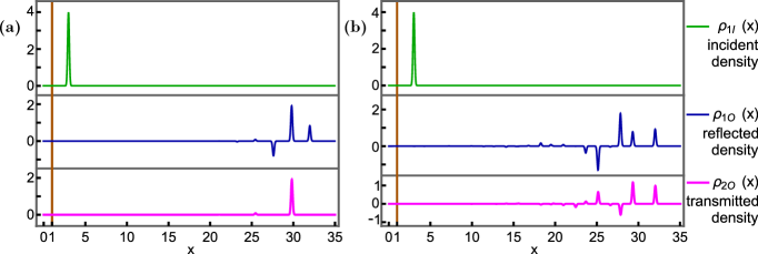
Figure 4: Density profiles with an interacting region extending from to 1 and total length of the QH edges 35 for a junction with taken to be one. The density profile is shown when the electron is injected from side, (a) with only intralayer interaction such that , and (b) with interlayer interactions, such that .
In this section, we take the complementary approach by studying the spatio-temporal evolution of an electron wave packet being injected at a point along the incoming QH edge. The injected wave packet is considered to have a Gaussian distribution: where ‘’ denotes the center of the injection point and ‘’ is the width of the injected wave packet. If the width of a single electron pulse is small compared to the length of the interacting region, i.e., , the electron wave packet fractionalizes into multiple pulses along the outgoing QH edges. Interestingly, in the presence of intralayer interaction alone (), no hole or negative pulse is reflected at the boundary in the transmitted edge channel (see fig. 4(a)). However, in the presence of interlayer interaction (), both the transmitted and reflected edge channels acquire fractionalized negative pulses in response to a positive incoming pulse (see fig. 4(b)). These fractionalized negative pulses in the transmitted edge channel can be considered as a signature of the presence of interlayer interaction in the system in the chiral time-resolved wave-packet measurement. In the long time limit, the density integral over the transmitted or reflected edge channel reduces to its DC value of the scattering matrix at , as expected, which adds up to one, confirming current conservation.