These authors contributed equally. \altaffiliationThese authors contributed equally. \alsoaffiliation[Present address: ]Institute of Physics, Czech Academy of Sciences, 162 00 Prague, Czech Republic
Demonstration of nonlocal Josephson effect in Andreev molecules
Abstract
We perform switching current measurements of planar Josephson junctions (JJs) coupled by a common superconducting electrode, with independent control over the two superconducting phase differences. We observe an anomalous phase shift in the current–phase relation of a JJ as a function of gate voltage or phase difference in the second JJ. This demonstrates a nonlocal Josephson effect, and the implementation of a -junction which is tunable both electrostatically and magnetically. The anomalous phase shift was larger for shorter distances between the JJs and vanished for distances much longer than the superconducting coherence length. Results are consistent with the hybridization of ABSs, leading to the formation of an Andreev molecule. Our devices constitute a realization of a tunable superconducting phase source, and could enable new coupling schemes for hybrid quantum devices.
Keywords: Hybrid materials, superconductor-semiconductor, Andreev bound state, Andreev molecule, -junction
The development of high-quality hybrid superconductor–semiconductor materials over the last decade enabled new possibilities in superconducting electronics and quantum computing 1, 2, 3. In particular, Andreev bound states (ABSs) 4, 5, 6 arising in superconductor–semiconductor–superconductor Josephson junctions (JJs) 7, 8, 9, 10 offer functionalities not attainable in metallic JJs. A prominent example is the electrostatic tuning of the critical current 11, 12, 3, which allows for JJ field-effect transistors 13, 14, 15, 16, voltage-tunable superconducting qubits 17, 18, 19, 20, resonators 21, 22 and amplifiers 23, 24, 25. Moreover, the interplay between ABSs, spin–orbit interaction and Zeeman fields results in non-reciprocal switching currents 26, 27, 28, 29 and anomalous phase offsets, or -junctions 30, 31, 32, 33, 34, 35, 36, 37, 38, with applications in superconducting electronics and spintronics 39.
A yet largely unexplored possibility offered by superconductor–semiconductor hybrids is the engineering of Andreev molecules from the hybridization of spatially overlapping ABSs 40, 41, 42, 43. Predicted to arise in JJs coupling over length scales comparable to the superconducting coherence length, Andreev molecules offer a promising platform to realize -junctions 40 and novel manipulation and coupling schemes for Andreev qubits 41. Experimental studies of ABS hybridization focused on two-terminal quantum dots 44, 45 and quantum dot chains 46. Recently, engineering of Andreev molecules was demonstrated in open, multiply connected geometries 47 and laterally coupled JJs 48, 49. Measurements of the switching current in double InAs nanowires revealed a nonlocal Josephson effect 48, however the device geometry did not allow measurements of phase shifts in the current–phase relation (CPR).
Here we demonstrate generation and electrical tuning of an anomalous phase shift in planar JJs that share a mesoscopic superconducting electrode. Inspired by Ref. 40, we realized devices consisting of two JJs sharing a common electrode and embedded in a superconducting double-loop geometry. The expected phase anomaly was ascribed 42 to the interplay between two distinct Cooper pair transfer mechanisms at and at , namely double crossed Andreev reflection (dCAR) and double elastic cotunneling (dEC), respectively. Differently from the proposal of Ref. 42, which considered semiconductor nanowires, we used planar JJs containing several ABSs. Such devices are lithographically defined with a top-down approach and, tuning their geometry, allow for large switching currents.
The double-loop geometry allowed us to independently tune the superconducting phase differences and across the two JJs, named JJ1 and JJ2, respectively. Furthermore, it allowed us to characterize the CPR of JJ1 for different values of . A coupling between JJ1 and JJ2 manifested as distorted and phase-shifted CPR of JJ1 for . Such a coupled system realizes the nonlocal Josephson effect: an anomalous phase shift (or, equivalently, an anomalous supercurrent at zero phase difference) was nonlocally induced in JJ1 by the phase difference across JJ2. Varying the length of the common superconducting electrode, we observed that the phase shift was larger for small , and vanished for much longer than the superconducting coherence length. Our observations are consistent with the hybridization of ABSs originating from the two JJs, resulting in the formation of an Andreev molecule. As the superconducting phase offset is electrically tuned by a current flowing in a flux line or a voltage applied to a gate, our devices constitute a demonstration of tunable superconducting phase source. Our findings open up new avenues for the design and implementation of advanced nanoscale quantum devices with enhanced controllability and functionality.
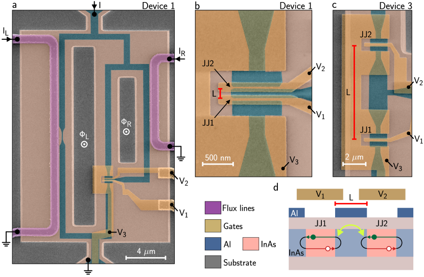
Experiments were performed on four devices (Devices 1 to 4) defined in the same epitaxial heterostructure of InAs and Al 3, 50, measured in a dilution refrigerator with a base temperature below . Figure 1(a) shows a false-colored scanning electron micrograph of Device 1, indicating the exposed InAs (pink), the epitaxial Al (blue), the gate electrodes (yellow) and the flux-bias lines (purple). Devices consisted of a small superconducting loop, threaded by the flux , embedded in the arm of a large superconducting loop, threaded by the flux . The region where the two loops merged [bottom right in Fig. 1(a)] is shown in Fig. 1(b). Here, three Al leads defined two nominally identical JJs which shared a central Al electrode of length . We label the bottom and top junction in Fig. 1(b) JJ1 and JJ2, respectively. In each JJ, the width of the Al electrodes was and the length of the junction was . From the junctions geometry, we estimate between to transverse modes to be present, for typical values of electron sheet density (see Supporting Information for details). Both JJ1 and JJ2 were controlled by gate electrodes, energized by voltages and , respectively. A third gate, at voltage , was set to throughout the experiment to prevent parallel conducting paths. A narrow Al constriction was defined on the left arm of the large Al loop [see Fig. 1(a)]. This constriction limited the maximum supercurrent flowing in the device, making switching current measurements feasible without warming up the apparatus. Devices 1 to 3 differed exclusively by the parameter , which was , and , respectively. Device 4 was lithographically identical to Device 1 and is presented in the Supporting Information, together with further details on the heterostructure and sample fabrication.
The measurement setup used to measure switching currents is schematically depicted in Fig. 1(a). After compensating for a global magnetic field offset using a vector magnet, local magnetic fluxes were generated by applying slowly varying currents and in the flux lines. Switching currents of the entire device were obtained by ramping the current from zero to around (depending on the device) with a repetition rate of , and detecting when the four-terminal voltage drop exceeded a threshold. As planar devices are characterized by an intrinsically large spread of their switching current 51, we averaged the results over ramps for each data point. In all of our devices, JJ1 had a maximum supercurrent of approximately , while the Al constrictions consistently showed switching currents of , independent of and . Due to the large asymmetry between the arms of the device, the switching current of the right arm was obtained by subtracting from the switching current of the entire device. Further details on the measurement setup are discussed in the Supporting Information.
Our devices allowed an independent tuning of the phase differences across the two junctions. The phase difference across JJ1 was tuned by the magnetic flux impinging within the perimeter of the device as , where is the superconducting magnetic flux quantum. The phase difference across JJ2 was instead tuned by the magnetic flux . However, as JJ2 was bypassed by a large stripe of Al, was not expected to affect , unless a nonlocal Josephson effect was present; in the absence of coupling between JJ1 and JJ2, would simply represent the CPR of JJ1.
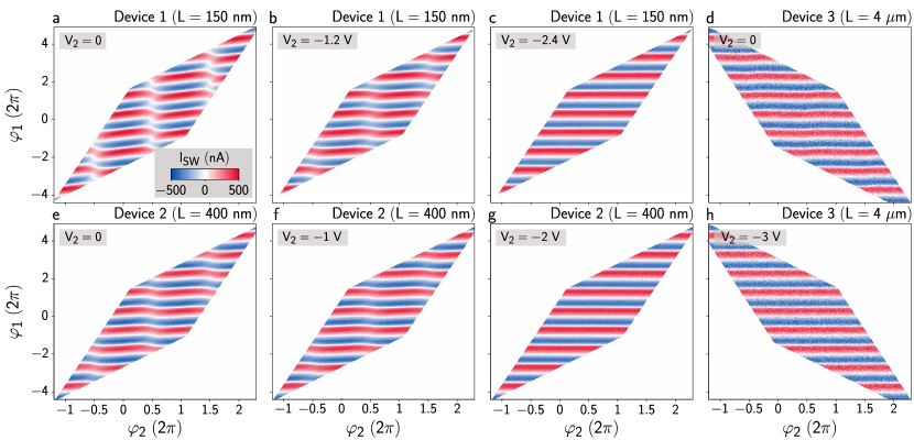
We further note that the finite geometric and kinetic inductances of the superconducting loops were too small to significantly distort the CPR of JJ1 and JJ2. Similarly, coupling between the two loops mediated by a shared inductance was negligible. The inductances of the inner and outer loops were and , respectively, while their common Al segment [right side of Fig. 1(a)] had an inductance of . Such values are significantly smaller than the Josephson inductances of JJ1 and JJ2, which were always greater than . The absence of inductive coupling was experimentally confirmed by results obtained on Device 3, as discussed below.
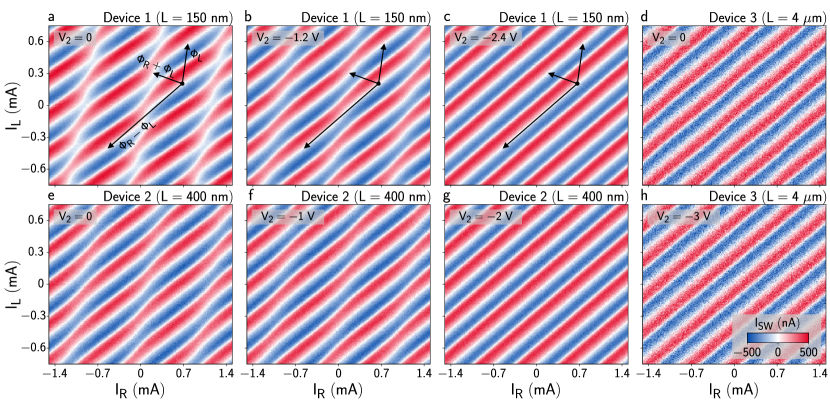
Figure 2(a) shows the switching current of Device 1 as a function of and and performed with and (both JJs open). Clear supercurrent oscillations were present, which depended on both and . The vector in Fig. 2(a) shows the direction over which is expected to be maximally modulated. The vectors and indicate the directions over which and are constant, respectively. Details on the definition of such vectors are presented in the Supporting Information. Clear modulations of the supercurrent were observed along , confirming a coupling between JJ1 and JJ2. Figures 2(b, c) show equivalent measurements performed after setting and , respectively. As was set more negative, JJ2 was depleted and the supercurrent oscillations became more and more regular, until supercurrent modulations were completely suppressed along [Fig. 2(c)] and JJ1 displayed a conventional forward-skewed CPR. Further, we note that did not alter the maximum switching current amplitude, confirming the absence of trivial electrostatic coupling between the gate of JJ2 and JJ1. Supercurrent measurements for Device 2, which had , are shown in Figs. 2 (e-g) for and varying . Anomalous phase modulations were still present in the supercurrent oscillations of Fig. 2(e), despite being significantly weaker than in Fig. 2(a). Setting [Fig. 2(g)] suppressed any remaining phase modulation, resulting in a conventional CPR as in Fig. 2(c). Finally, Figs. 2(d, h) show measurements performed in Device 3, with . In this case, phase modulations never occurred along , neither for [Fig. 2(d)] nor when [Fig. 2(h)], demonstrating the absence of coupling in well-separated JJs and that contributions of loop inductance and circulating currents to phase shifts were negligible.
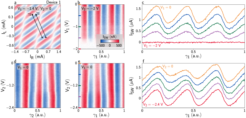
Figure 3 presents the dependence of supercurrent oscillations in Device 1 on and . Panel (a) shows supercurrent oscillations for and : while the oscillation amplitude was reduced by setting negative, the oscillation pattern was almost identical to that of Fig. 2(a), indicating that had negligible influence on the anomalous phase shift. The effect of gate voltages was further investigated by measuring supercurrents along the paths and , shown as arrows in Fig. 3(a). Figure 3(b) shows the CPR of JJ1 measured along with , that is with no current flowing in JJ2. Selected linecuts are plotted in Fig. 3(c). Again, we note that did not induce a phase shift, but simply decreased the oscillation amplitude until no current flowed in the right arm of the device. The linecuts in Fig. 3(c) demonstrate that JJ1 had a forward-skewed CPR, which can be parameterized by an effective junction transmission of , indicating the presence of highly transmissive ABSs in JJ1 (see Supporting Information for details). Figures 3(d, e) show the CPR of JJ1 along and , respectively, measured for . Selected linecuts of Fig. 3(e) are shown in Fig. 3(f). Both Figs. 3(d) and (e) show distorted and phase-shifted supercurrent oscillations which evolved with decreasing , saturating to a conventional forward-skewed CPR for .
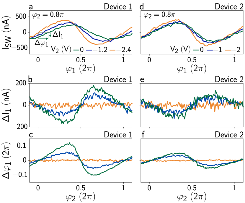
Figure 4 summarizes the main results of this work. After performing an appropriate basis transformation to the data in Figs. 2(a-c), it is possible to display as a function of for selected values of [see Supporting Information for details]. For example, Fig. 4(a) shows for , that is when the phase shift was found to be the largest. Figure 4(a) also highlights the quantities and , which represent the anomalous supercurrent (i.e., the supercurrent at ) and anomalous phase shift, respectively. The dependence of and on are further shown in Figs. 4(b) and (c). Similar results for Device 2 are shown in Fig. 4(d-f). The data presented here demonstrates coupling between the JJs, consistent with the formation of an Andreev molecule from the ABSs of JJ1 and JJ2 40. Time-reversal symmetry requires , which imposes at . This condition was used to accurately account for a constant offset to . For , the CPR of JJ1 gained an anomalous phase shift or, equivalently, an anomalous supercurrent at , controlled by both phase and gate tuning of JJ2. Both the anomalous phase shift and anomalous supercurrent were symmetric and periodic in , consistent with theoretical expectations 40. The phase shift was also an odd function of , consistent with the relative interplay of dCAR and dEC processes as a function of the nonlocal phase. There was also a pronounced forward skewness to , which is a consequence of the nonsinusoidal CPR of both JJs. The largest measured in Device 1 was , which resulted in . These values might be increased further in devices with shorter . We confirmed that coupling takes place over length scales of at least , but significantly smaller than . Such length scales are consistent with those of superconducting correlations in our devices. In the InAs quantum well, we expect a superconducting coherence length 52, compared to of the Al film 53. These length scales are compatible with the absence of coupling in Device 3 (), and they indicate that both the semiconductor and the superconductor might be relevant to mediate the coupling over short JJ separations. Extending our experiments to several devices with varying will make it possible to extract the typical length scale governing the nonlocal effect, thus providing a better understanding of the microscopic coupling mechanisms.
Further insights into the non-local Josephson effect are gained via the gate dependence shown in Fig. 3. Data indicates that affected the amplitude of but not , while tuned without any influence on the amplitude of . A gate-dependent phase shift can result from tuning of the transmission and number of ABSs in each JJ, affecting the degree of hybridization between ABSs in JJ1 and JJ2. If the gate tuning of was only due to a change of the ABS transmissions as a function of , we would expect the effect to be symmetric with respect to JJ1 and JJ2, contrary to the observations. Previous work also showed that gate voltages mainly affect hybrid JJs by reducing the number of ABSs, not by changing the ABS transmission 54. We instead speculate that the different dependence of on and reflects how is affected by the number of ABSs present in each junction. In the present case, controls by tuning the number of ABSs in JJ2 available for hybridizing with the ABSs in JJ1. As JJ2 is depleted, ABSs in JJ1 progressively lose states of JJ2 to hybridize with, until a conventional CPR is restored. On the other hand, setting negative decreases the number of ABSs in JJ1, which directly results in a decrease of . However, as long as the number of ABSs in JJ2 is unchanged, the hybridization of the remaining ABSs in JJ1 is also unchanged and remains constant.
Previous work demonstrated -junction behavior in the same material system by the combination of spin–orbit coupling and external magnetic fields 37. To achieve similar as in Fig. 4(c), in-plane magnetic fields of approximately were required. Such magnetic fields are hardly compatible with existing superconducting electronics, making the nonlocal Josephson effect mediated by Andreev molecules a particularly promising avenue to generate arbitrary phase shifts in superconducting devices. Another recent work showed a persistent -junction behavior induced by ferromagnetic elements in a JJ and field cycling, constituting a phase battery 38; the -junction that we realized here is instead continuously and electrically tunable over short times scales, hence it could be promptly utilized as a phase source for applications in superconducting electronics and spintronics.
In conclusion, our investigation of phase-tunable JJs placed in close proximity to each other and sharing a common electrode demonstrated the formation of an Andreev molecule exhibiting nonlocal Josephson effect. This manifested as an anomalous phase shift and an anomalous supercurrent arising in one JJ, depending on phase tuning and gating of the second JJ. In the light of our results, Andreev molecules expand the available toolset of functionality in hybrid materials, also enabling new quantum manipulation schemes and coupling architectures for hybrid qubits.
Note: during the final preparation of this manuscript, a paper reporting very similar effects was posted online 55.
1 Supporting Information
Supporting Information includes: a detailed discussion on sample fabrication and electrical measurements; calculations of the superconducting coherence length, loop inductances and the effective junction transmission; details on current-to-flux conversion; and additional experimental results on Device 4, which was identical to Device 1.
2 Acknowledgments
We thank the Cleanroom Operations Team of the Binnig and Rohrer Nanotechnology Center (BRNC) for their help and support. We are grateful to H. Weisbrich and J.C. Cuevas for useful discussions. W.B. acknowledges support from the DFG via SFB 1432 (ID 425217212) and BE 3803/14-1 (ID 467596333). W.W. acknowledges support from the Swiss National Science Foundation (grant number 200020_207538). F.N. acknowledges support from the European Research Council (grant number 804273) and the Swiss National Science Foundation (grant number 200021_201082).
References
- Krogstrup et al. 2015 Krogstrup, P.; Ziino, N. L. B.; Chang, W.; Albrecht, S. M.; Madsen, M. H.; Johnson, E.; Nygård, J.; Marcus, C.; Jespersen, T. S. Epitaxy of semiconductor-superconductor nanowires. Nat. Mater. 2015, 14, 400–406
- Chang et al. 2015 Chang, W.; Albrecht, S. M.; Jespersen, T. S.; Kuemmeth, F.; Krogstrup, P.; Nygård, J.; Marcus, C. M. Hard gap in epitaxial semiconductor-superconductor nanowires. Nat. Nanotechnol. 2015, 10, 232–236
- Shabani et al. 2016 Shabani, J.; Kjaergaard, M.; Suominen, H. J.; Kim, Y.; Nichele, F.; Pakrouski, K.; Stankevic, T.; Lutchyn, R. M.; Krogstrup, P.; Feidenhans’l, R.; Kraemer, S.; Nayak, C.; Troyer, M.; Marcus, C. M.; Palmstrøm, C. J. Two-dimensional epitaxial superconductor-semiconductor heterostructures: A platform for topological superconducting networks. Phys. Rev. B 2016, 93, 155402
- Andreev 1964 Andreev, A. F. Thermal conductivity of the intermediate state of superconductors. Sov. Phys. JETP 1964, 19, 1228–1231
- Beenakker and van Houten 1991 Beenakker, C. W. J.; van Houten, H. Josephson current through a superconducting quantum point contact shorter than the coherence length. Phys. Rev. Lett. 1991, 66, 3056–3059
- Furusaki and Tsukada 1991 Furusaki, A.; Tsukada, M. Current-carrying states in Josephson junctions. Phys. Rev. B 1991, 43, 10164–10169
- Pillet et al. 2010 Pillet, J.-D.; Quay, C. H. L.; Morfin, P.; Bena, C.; Yeyati, A. L.; Joyez, P. Andreev bound states in supercurrent-carrying carbon nanotubes revealed. Nat. Phys. 2010, 6, 965–969
- Bretheau et al. 2013 Bretheau, L.; Girit, Ç. Ö.; Urbina, C.; Esteve, D.; Pothier, H. Supercurrent Spectroscopy of Andreev States. Phys. Rev. X 2013, 3, 041034
- Tosi et al. 2019 Tosi, L.; Metzger, C.; Goffman, M. F.; Urbina, C.; Pothier, H.; Park, S.; Yeyati, A. L.; Nygård, J.; Krogstrup, P. Spin–orbit splitting of Andreev states revealed by microwave spectroscopy. Phys. Rev. X 2019, 9, 011010
- Nichele et al. 2020 Nichele, F.; Portolés, E.; Fornieri, A.; Whiticar, A. M.; Drachmann, A. C. C.; Gronin, S.; Wang, T.; Gardner, G. C.; Thomas, C.; Hatke, A. T.; Manfra, M. J.; Marcus, C. M. Relating Andreev bound states and supercurrents in hybrid Josephson junctions. Phys. Rev. Lett. 2020, 124, 226801
- Doh et al. 2005 Doh, Y.-J.; van Dam, J. A.; Roest, A. L.; Bakkers, E. P. A. M.; Kouwenhoven, L. P.; Franceschi, S. D. Tunable supercurrent through semiconductor nanowires. Science 2005, 309, 272–275
- Xiang et al. 2006 Xiang, J.; Vidan, A.; Tinkham, M.; Westervelt, R. M.; Lieber, C. M. Ge/Si nanowire mesoscopic Josephson junctions. Nat. Nanotechnol. 2006, 1, 208–213
- Gheewala 1980 Gheewala, T. Josephson-logic devices and circuits. IEEE Trans. Electron Devices 1980, 27, 1857–1869
- Clark et al. 1980 Clark, T. D.; Prance, R. J.; Grassie, A. D. C. Feasibility of hybrid Josephson field effect transistors. J. Appl. Phys. 1980, 51, 2736
- Kleinsasser and Jackson 1989 Kleinsasser, A.; Jackson, T. Prospects for proximity effect superconducting FETs. IEEE Trans. Magn. 1989, 25, 1274–1277
- Wen et al. 2019 Wen, F.; Shabani, J.; Tutuc, E. Josephson junction field-effect transistors for boolean logic cryogenic applications. IEEE Trans. Electron Devices 2019, 66, 5367–5374
- Larsen et al. 2015 Larsen, T. W.; Petersson, K. D.; Kuemmeth, F.; Jespersen, T. S.; Krogstrup, P.; Nygård, J.; Marcus, C. M. Semiconductor-nanowire-based superconducting qubit. Phys. Rev. Lett. 2015, 115, 127001
- de Lange et al. 2015 de Lange, G.; van Heck, B.; Bruno, A.; van Woerkom, D. J.; Geresdi, A.; Plissard, S. R.; Bakkers, E. P. A. M.; Akhmerov, A. R.; DiCarlo, L. Realization of microwave quantum circuits using hybrid superconducting-semiconducting nanowire Josephson elements. Phys. Rev. Lett. 2015, 115, 127002
- Casparis et al. 2018 Casparis, L.; Connolly, M. R.; Kjaergaard, M.; Pearson, N. J.; Kringhøj, A.; Larsen, T. W.; Kuemmeth, F.; Wang, T.; Thomas, C.; Gronin, S.; Gardner, G. C.; Manfra, M. J.; Marcus, C. M.; Petersson, K. D. Superconducting gatemon qubit based on a proximitized two-dimensional electron gas. Nat. Nanotechnol. 2018, 13, 915–919
- Pita-Vidal et al. 2020 Pita-Vidal, M.; Bargerbos, A.; Yang, C.-K.; van Woerkom, D. J.; Pfaff, W.; Haider, N.; Krogstrup, P.; Kouwenhoven, L. P.; de Lange, G.; Kou, A. Gate-tunable field-compatible fluxonium. Phys. Rev. Appl. 2020, 14, 064038
- Casparis et al. 2019 Casparis, L.; Pearson, N. J.; Kringhøj, A.; Larsen, T. W.; Kuemmeth, F.; Nygård, J.; Krogstrup, P.; Petersson, K. D.; Marcus, C. M. Voltage-controlled superconducting quantum bus. Phys. Rev. B 2019, 99, 085434
- Sardashti et al. 2020 Sardashti, K.; Dartiailh, M. C.; Yuan, J.; Hart, S.; Gumann, P.; Shabani, J. Voltage-tunable superconducting resonators: a platform for random access quantum memory. IEEE Trans. Quantum Eng. 2020, 1, 1–7
- Butseraen et al. 2022 Butseraen, G.; Ranadive, A.; Aparicio, N.; Rafsanjani Amin, K.; Juyal, A.; Esposito, M.; Watanabe, K.; Taniguchi, T.; Roch, N.; Lefloch, F.; Renard, J. A gate-tunable graphene Josephson parametric amplifier. Nat. Nanotechnol. 2022, 17, 1153–1158
- Sarkar et al. 2022 Sarkar, J.; Salunkhe, K. V.; Mandal, S.; Ghatak, S.; Marchawala, A. H.; Das, I.; Watanabe, K.; Taniguchi, T.; Vijay, R.; Deshmukh, M. M. Quantum-noise-limited microwave amplification using a graphene Josephson junction. Nat. Nanotechnol 2022, 17, 1147–1152
- Phan et al. 2022 Phan, D.; Falthansl-Scheinecker, P.; Mishra, U.; Strickland, W. M.; Langone, D.; Shabani, J.; Higginbotham, A. P. Gate-tunable, superconductor-semiconductor parametric amplifier. arXiv:2206.05746, 2022
- Baumgartner et al. 2022 Baumgartner, C.; Fuchs, L.; Costa, A.; Reinhardt, S.; Gronin, S.; Gardner, G. C.; Lindemann, T.; Manfra, M. J.; Faria Junior, P. E.; Kochan, D.; Fabian, J.; Paradiso, N.; Strunk, C. Supercurrent rectification and magnetochiral effects in symmetric Josephson junctions. Nat. Nanotechnol. 2022, 17, 39–44
- Turini et al. 2022 Turini, B.; Salimian, S.; Carrega, M.; Iorio, A.; Strambini, E.; Giazotto, F.; Zannier, V.; Sorba, L.; Heun, S. Josephson diode effect in high-mobility InSb nanoflags. Nano Lett. 2022, 22, 8502–8508
- Gupta et al. 2023 Gupta, M.; Graziano, G. V.; Pendharkar, M.; Dong, J. T.; Dempsey, C. P.; Palmstrøm, C.; Pribiag, V. S. Gate-tunable superconducting diode effect in a three-terminal Josephson device. Nat. Commun. 2023, 14, 3078
- Matsuo et al. 2023 Matsuo, S.; Imoto, T.; Yokoyama, T.; Sato, Y.; Lindemann, T.; Gronin, S.; Gardner, G. C.; Manfra, M. J.; Tarucha, S. Josephson diode effect derived from short-range coherent coupling. arXiv:2305.07923, 2023
- Buzdin and Koshelev 2003 Buzdin, A.; Koshelev, A. E. Periodic alternating 0- and -junction structures as realization of -Josephson junctions. Phys. Rev. B 2003, 67, 220504
- Buzdin 2008 Buzdin, A. Direct coupling between magnetism and superconducting current in the Josephson junction. Phys. Rev. Lett. 2008, 101, 107005
- Yokoyama et al. 2014 Yokoyama, T.; Eto, M.; Nazarov, Y. V. Anomalous Josephson effect induced by spin-orbit interaction and Zeeman effect in semiconductor nanowires. Phys. Rev. B 2014, 89, 195407
- Bergeret and Tokatly 2015 Bergeret, F. S.; Tokatly, I. V. Theory of diffusive -0 Josephson junctions in the presence of spin-orbit coupling. EPL 2015, 110, 57005
- Szombati et al. 2016 Szombati, D. B.; Nadj-Perge, S.; Car, D.; Plissard, S. R.; Bakkers, E. P. A. M.; Kouwenhoven, L. P. Josephson -junction in nanowire quantum dots. Nat. Phys. 2016, 12, 568–572
- Hart et al. 2017 Hart, S.; Ren, H.; Kosowsky, M.; Ben-Shach, G.; Leubner, P.; Brüne, C.; Buhmann, H.; Molenkamp, L. W.; Halperin, B. I.; Yacoby, A. Controlled finite momentum pairing and spatially varying order parameter in proximitized HgTe quantum wells. Nat. Phys. 2017, 13, 87–93
- Assouline et al. 2019 Assouline, A.; Feuillet-Palma, C.; Bergeal, N.; Zhang, T.; Mottaghizadeh, A.; Zimmers, A.; Lhuillier, E.; Eddrie, M.; Atkinson, P.; Aprili, M.; Aubin, H. Spin–orbit induced phase-shift in Bi2Se3 Josephson junctions. Nat. Commun. 2019, 10, 126
- Mayer et al. 2020 Mayer, W.; Dartiailh, M. C.; Yuan, J.; Wickramasinghe, K. S.; Rossi, E.; Shabani, J. Gate controlled anomalous phase shift in Al/InAs Josephson junctions. Nat. Commun. 2020, 11, 212
- Strambini et al. 2020 Strambini, E.; Iorio, A.; Durante, O.; Citro, R.; Sanz-Fernández, C.; Guarcello, C.; Tokatly, I. V.; Braggio, A.; Rocci, M.; Ligato, N.; Zannier, V.; Sorba, L.; Bergeret, F. S.; Giazotto, F. A Josephson phase battery. Nat. Nanotechnol. 2020, 15, 656–660
- Linder and Robinson 2015 Linder, J.; Robinson, J. W. A. Superconducting spintronics. Nat. Phys. 2015, 11, 307–315
- Pillet et al. 2019 Pillet, J.-D.; Benzoni, V.; Griesmar, J.; Smirr, J.-L.; Girit, Ç. O. Nonlocal Josephson effect in Andreev molecules. Nano Lett. 2019, 19, 7138–7143
- Kornich et al. 2019 Kornich, V.; Barakov, H. S.; Nazarov, Y. V. Fine energy splitting of overlapping Andreev bound states in multiterminal superconducting nanostructures. Phys. Rev. Res. 2019, 1, 033004
- Pillet et al. 2020 Pillet, J.-D.; Benzoni, V.; Griesmar, J.; Smirr, J.-L.; Girit, Ç. Scattering description of Andreev molecules. SciPost Phys. Core 2020, 2, 009
- Kornich et al. 2020 Kornich, V.; Barakov, H. S.; Nazarov, Y. V. Overlapping Andreev states in semiconducting nanowires: Competition of one-dimensional and three-dimensional propagation. Phys. Rev. B 2020, 101, 195430
- Su et al. 2017 Su, Z.; Tacla, A. B.; Hocevar, M.; Car, D.; Plissard, S. R.; Bakkers, E. P. A. M.; Daley, A. J.; Pekker, D.; Frolov, S. M. Andreev molecules in semiconductor nanowire double quantum dots. Nat. Commun. 2017, 8, 585
- Kürtössy et al. 2021 Kürtössy, O.; Scherübl, Z.; Fülöp, G.; Lukács, I. E.; Kanne, T.; Nygård, J.; Makk, P.; Csonka, S. Andreev molecule in parallel InAs nanowires. Nano Lett. 2021, 21, 7929–7937
- Dvir et al. 2023 Dvir, T. et al. Realization of a minimal Kitaev chain in coupled quantum dots. Nature 2023, 614, 445–450
- Coraiola et al. 2023 Coraiola, M.; Haxell, D. Z.; Sabonis, D.; Weisbrich, H.; Svetogorov, A. E.; Hinderling, M.; ten Kate, S. C.; Cheah, E.; Krizek, F.; Schott, R.; Wegscheider, W.; Cuevas, J. C.; Belzig, W.; Nichele, F. Hybridisation of Andreev bound states in three-terminal Josephson junctions. arXiv:2302.14535, 2023
- Matsuo et al. 2022 Matsuo, S.; Lee, J. S.; Chang, C.-Y.; Sato, Y.; Ueda, K.; Palmstrøm, C. J.; Tarucha, S. Observation of nonlocal Josephson effect on double InAs nanowires. Commun. Phys. 2022, 5, 221
- Matsuo et al. 2023 Matsuo, S.; Imoto, T.; Yokoyama, T.; Sato, Y.; Lindemann, T.; Gronin, S.; Gardner, G. C.; Nakosai, S.; Tanaka, Y.; Manfra, M. J.; Tarucha, S. Phase-dependent Andreev molecules and superconducting gap closing in coherently coupled Josephson junctions. arXiv:2303.10540, 2023
- Cheah et al. 2023 Cheah, E.; Haxell, D. Z.; Schott, R.; Zeng, P.; Paysen, E.; Kate, S. C. t.; Coraiola, M.; Landstetter, M.; Zadeh, A. B.; Trampert, A.; Sousa, M.; Riel, H.; Nichele, F.; Wegscheider, W.; Krizek, F. Control over epitaxy and the role of the InAs/Al interface in hybrid two-dimensional electron gas systems. arXiv:2301.06795, 2023
- Haxell et al. 2023 Haxell, D. Z.; Cheah, E.; Křížek, F.; Schott, R.; Ritter, M. F.; Hinderling, M.; Belzig, W.; Bruder, C.; Wegscheider, W.; Riel, H.; Nichele, F. Measurements of phase dynamics in planar Josephson junctions and SQUIDs. Phys. Rev. Lett. 2023, 130, 087002
- 52 See the Supplemental Material for a detailed discussion on sample fabrication and electrical measurements, and for additional experimental results.
- van Woerkom et al. 2017 van Woerkom, D. J.; Proutski, A.; van Heck, B.; Bouman, D.; Väyrynen, J. I.; Glazman, L. I.; Krogstrup, P.; Nygård, J.; Kouwenhoven, L. P.; Geresdi, A. Microwave spectroscopy of spinful Andreev bound states in ballistic semiconductor Josephson junctions. Nat. Phys. 2017, 13, 876–881
- Kjaergaard et al. 2017 Kjaergaard, M.; Suominen, H. J.; Nowak, M. P.; Akhmerov, A. R.; Shabani, J.; Palmstrøm, C. J.; Nichele, F.; Marcus, C. M. Transparent semiconductor–superconductor interface and induced gap in an epitaxial heterostructure Josephson junction. Phys. Rev. Appl. 2017, 7, 034029
- Matsuo et al. 2023 Matsuo, S.; Imoto, T.; Yokoyama, T.; Sato, Y.; Lindemann, T.; Gronin, S.; Gardner, G. C.; Manfra, M. J.; Tarucha, S. Engineering of anomalous Josephson effect in coherently coupled Josephson junctions. arXiv:2305.06596, 2023
- Annunziata et al. 2010 Annunziata, A. J.; Santavicca, D. F.; Frunzio, L.; Catelani, G.; Rooks, M. J.; Frydman, A.; Prober, D. E. Tunable superconducting nanoinductors. Nanotechnology 2010, 21, 445202
3 Materials and Methods
The heterostructure used in this work was grown with molecular beam epitaxy techniques on an InP (001) substrate. The top part of the heterostructure consisted of a step-graded InAlAs buffer, and an thick InAs quantum well confined between two barriers. The bottom and top barriers were and thick, respectively. On top of the III–V stack, two monolayers of GaAs and a thick Al layer were deposited in situ, without breaking vacuum. Characterization of the 2DEG in a Hall bar geometry revealed a peak mobility of at an electron sheet density of . This resulted in an electron mean free path , indicating that Josephson junctions in our devices were in the ballistic regime. The superconducting coherence length in InAs was calculated as . Here is the reduced Plank constant, is the electron Fermi velocity, and is the induced superconducting gap in InAs, which we consider similar to that of bulk Al. Fabrication of the devices was conducted in an identical manner to that described in Ref. 47.
The Al film had a kinetic inductance of per unit square, calculated from a superconducting Hall bar in the same material 56, 47. The geometric and kinetic inductance contributions are calculated for the outer [ in Fig. 1(a) of the Main Text] and inner [ in Fig. 1(a) of the Main Text] loops. The values for the outer (inner) loop were () for the geometric inductance and () for the kinetic inductance. The portion of the circuit shared by both loops, corresponding to the right branch in Fig. 1(a) of the Main Text, had a kinetic inductance of and a geometric inductance of .
Josephson junctions (JJs) were identical in design for all devices. From the junction geometry, the approximate number of transverse modes sustained by the junction is , where is the Fermi wavelength. From gated Hall bar measurements, the sheet carrier density is expected to vary in a range – for typical values of top-gate voltage. This gives a Fermi wavelength of between and , implying a number of modes between and . Measurements of the current–phase relation (CPR) in JJ1 of Device 1 [Fig. 3(b) of the Main Text] show a non-sinusoidal CPR, indicating the presence of highly transparent modes. The CPR at [see Fig. 3(c) of the Main Text] gives an effective junction transmission of over an effective number of highly-transmissive modes 10. For , was approximately constant.
Electrical measurements were performed in a dilution refrigerator with a mixing chamber base temperature below . Electrical contacts to each device, except for the two flux lines, were provided by resistive looms with QDevil pi-filters at the mixing chamber level and RC filters at both mixing chamber and sample stage. The bias current passing through the devices was sourced via a Keysight 33600 Waveform Generator. The two output channels produced two synchronized and opposite voltage sawtooth waveforms with amplitude of about (depending on the specific device) and repetition rate of . The two waveforms were applied via two resistors placed in series to device source and drain contact, resulting in a maximum current of approximately . The voltage drop across the device was measured in a four-terminal configuration via a home-made differential amplifier with a gain of 1000, a further amplification stage of 42 provided by the internal amplifier of a Standford Research SR860 lock-in amplifier, and finally detected by a Keysight DSOX2024A oscilloscope. The oscilloscope measured the time needed for the voltage drop across the device to overcome a threshold, set at of the maximum voltage measured in the resistive state. The switching time was averaged over 16 current ramps and converted into a current. With these measurement parameters, transition from superconducting to resistive state was extremely sharp, making the exact choice of the experimental parameters irrelevant. Flux lines were connected via a superconducting loom, with pi-filters at the mixing chamber level to suppress high-frequency noise, resulting in a total line resistances below . Currents and were generated by two Yokogawa GS200 sources set to current mode. Low-pass RC filters with and were placed at the current source output.
4 Current-to-Phase Conversion
As described in the Main Text, currents and were injected into flux bias lines proximal to the device. Each current generated a magnetic field, predominantly impinging on the closest loop: mainly controlled an external flux threading the left loop, and mainly controlled an external flux through the right loop. Nevertheless, each flux line had a finite coupling to the furthest loop, meaning that and depended on both and . The phase difference across JJ1, , changed most strongly as a result of a flux threading the outer loop of the device [see Fig. 1(a) of the Main Text], which corresponds to . This is because a path along the outer loop contains only JJ1 (and the Al constriction), so the phase difference across JJ1 was proportional to the flux threading that area. We note that the arrow labeled in Fig. 2(a) of the Main Text corresponds to . The phase difference was constant along the direction, since any increase in the flux through one loop was compensated by the flux through the other. We apply the same procedure to JJ2, showing that the phase across JJ2 varied most strongly as a function of and was constant along the direction. We define the phase axes as those along which only one phase varies, meaning corresponds to and corresponds to . We therefore define these as our phase axes, and perform the conversion from () to () using the relation:
| (1) |
where is the superconducting flux quantum and is a matrix relating the flux line currents () to the fluxes (). We calculate for each device, using the switching current measurements taken at [see Figs. 2(a) and (e) of the Main Text for Devices 1 and 2, respectively]. We evaluate Eq. 1 for and , and thereby obtain:
| (2) |
for Device 1 and
| (3) |
for Device 2. The good agreement between Eqs. 2 and 3 show that the loop sizes and the flux line fabrication was almost identical between Devices 1 and 2. The matrix from Eq. 2 was used for Device 3, where independent evaluation was not possible due to the presence of only two periodicity axes. The position of was defined where the line intersected all flux periodicity axes, for increasing in the direction. Using the matrix of Eq. 2 or 3, we apply the linear transformation of Eq. 1 to convert the axes to . The result is plotted in Fig. S.1, for the data presented in Fig. 2 of the Main Text.
Linecuts of the data in Fig. S.1 along are plotted in Fig. 4(a, d) of the Main Text, at . The anomalous switching current , plotted in Fig. 4(b, e) of the Main Text, was obtained as a linecut of the data in Fig. S.1 along , for . To account for small misalignment of the origin with respect to the data, a constant switching current offset was subtracted from each dataset such that the oscillations in were symmetric. Anomalous phase shifts were calculated from the position where , as a function of . Phase shifts were calculated relative to the data where no current flowed through JJ2 ( for Device 1, for Device 2). We expect a symmetric deviation in phase across a full period, so a small constant offset was independently obtained and subtracted from each dataset such that the oscillations in were symmetric.
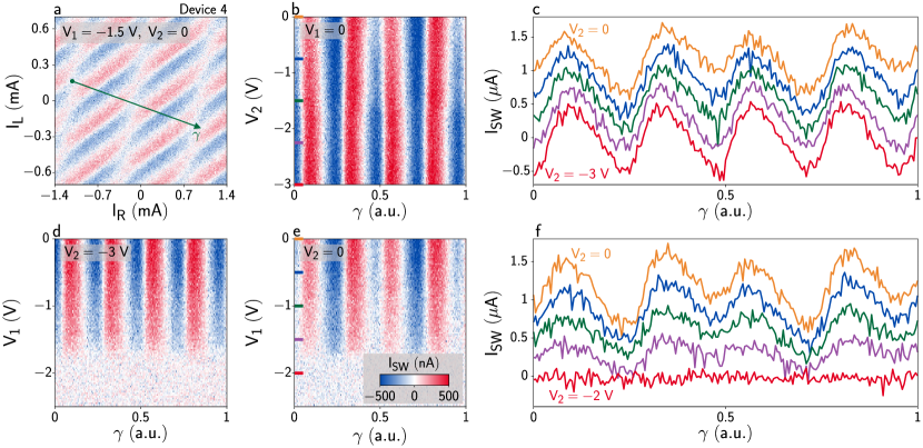
5 Measurements on Device 4
Measurements were performed on a fourth device, identical in design to Device 1 (). Switching current measurements of Device 4 are summarized in Fig. S.2, after subtracting a background corresponding to the switching current of the Al constriction, . The switching current was measured as a function of the current injected into the left and right flux lines, and . The currents () correspond to fluxes () threading the left and right loops, respectively. The phase difference across JJ1, , is expected to be modulated most strongly for fluxes threading both loops, i.e., . In the case of no coupling between the JJs, is expected to be constant as a function of . The phase difference across JJ2 is constant as a function of . These directions are indicated on Fig. S.2(a) as the black arrows. When [Fig. S.2(a)], there is a clear distortion of the switching current away from the phase axes, indicating hybridization with JJ2. From Fig. S.2(a), the size and shape of this distortion is qualitatively similar to that of Device 1 in the same gate configuration [Fig. 2(a) of the Main Text]. Figure S.2(b) shows the switching current as a function of phase differences across the JJs, (), obtained using the same method outlined in Eq. 1. The transformation matrix for Device 4 was:
Measurements were performed for different gate voltages applied to JJ2: for Fig. S.2(c) and for Fig. S.2(e). Figures S.2(d) and (f) show the switching current after transformation by matrix , for Figs. S.2(c) and (e) respectively. When JJ2 was partially depleted, but still allowed a current to flow, there was a distortion of but it was less pronounced than for . For , where no current could flow through the fully closed JJ2, there was no distortion of the switching current from the direction and oscillations in occurred with a single periodicity axis. In this configuration, there was no coupling between JJs and the current-phase relation (CPR) was that of JJ1 alone.
The anomalous switching current at is plotted in Fig. S.2(g) as a function of , for different gate voltages [colors]. A large, -dependent anomalous switching current was observed for , which was smaller for and absent for . The phase shift is quantified in Fig. S.2(h), as a function of for different gate voltages . The maximum phase shift for was at , almost identical to the result of Device 1. The size of the phase shift was smaller for more negative , and completely suppressed when JJ2 was closed.
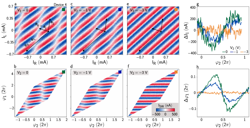
Figure S.3 presents the dependence of the switching current of Device 4 on the gate voltages and . Figure S.3(a) shows as a function of flux line currents and , for and . While the oscillation amplitude was reduced relative to the configuration, the switching current modulation was comparable to that of Fig. S.2(a). The switching current was measured along the path , parallel to the direction. Figure S.3(b) shows along as a function of , with . Selected linecuts are shown in Fig. S.3(c). The position of shifted as a function of and the oscillations changed from being distorted for , to a regularly skewed CPR for . This demonstrates the strong effect of on the CPR of JJ1. Figures S.3(d) and (e) show along as a function of , for and respectively. The switching current had a conventional forward-skewed CPR in Fig. S.3(d), since no current flowed through JJ2. Decreasing only decreased the amplitude of oscillations. For , a current flowed through JJ2. Nevertheless, only caused a decrease in the overall amplitude of oscillations, without introducing distortions or phase shifts. This is also evident from selected linecuts, displayed in Fig. S.3(f), showing that had little to no effect on the anomalous phase shift .