Electronic structure of few-layer black phosphorus from -ARPES
Abstract
Black phosphorus (BP) stands out among two-dimensional (2D) semiconductors because of its high mobility and thickness dependent direct band gap. However, the quasiparticle band structure of ultrathin BP has remained inaccessible to experiment thus far. Here we use a recently developed laser-based micro-focus angle resolved photoemission (-ARPES) system to establish the electronic structure of 2–9 layer BP from experiment. Our measurements unveil ladders of anisotropic, quantized subbands at energies that deviate from the scaling observed in conventional semiconductor quantum wells. We quantify the anisotropy of the effective masses and determine universal tight-binding parameters which provide an accurate description of the electronic structure for all thicknesses.
Few-layer black phosphorus (BP) has an interesting combination of properties and attracts attention for applications in electronics, photonics and sensing [1, 2, 3]. In contrast to transition metal dichalcogenides (TMDs), the gap of BP remains direct for any thickness and decreases more rapidly from eV in the monolayer down to eV in bulk-like samples spanning the entire technologically relevant mid-infrared range [4, 5, 6, 7, 8, 9, 10]. Light emission from BP is linearly polarized [11, 12] and can be tuned by strain [13, 14, 3] and gating [15, 16, 17, 18] over a wide range that includes telecommunications bands. This has been exploited for gas sensing [3], tuneable infrared lasers [19], variable spectrum detectors and optoelectronic modulators [20, 17, 3].
BP is less air-stable than transition metal dichalcogenides (TMDs) [21, 22] but encapsulation between inert 2D materials was found to be very effective in preventing degradation [23, 24]. Few-layer BP devices with carefully protected interfaces achieved low-temperature mobilities far in excess of TMDs [25, 26, 27, 28]. This enabled the first observation of the integer and fractional quantum Hall effect in a 2D material other than graphene [28, 27]. However, the insight into BP device properties is not yet comparable to graphene, not least because it proved more difficult to establish a tight-binding description of the single particle electronic structure of BP and to determine the relevant parameters.
The electronic structure of BP is more complex than that of few-layer graphene and remains largely unexplored by experiment. Monolayer BP consists of puckered honeycomb units, which results in a rectangular unit cell with 4 basis atoms, each contributing 5 electrons distributed in a complex, momentum-dependent way over the 4 orbitals of phosphorus [29, 30, 31, 6]. It is thus not a-priori clear how to construct a simple, yet accurate effective model of the electronic structure of BP. Theoretical studies found that the valence band maximum (VBM) of bulk BP has dominant orbital character. This motivated the development of an effective single-orbital tight-binding model of few-layer BP for the relevant states near the Brillouin zone center [30, 31, 32]. However, because of the puckered structure of BP, even a single orbital model requires an important number of parameters. While a good description of few-layer graphene is obtained with only 2 tight-binding parameters, theoretical work on BP used 14 parameters to obtain a precise parametrization of first-principles calculations [31, 32]. Moreover, such calculations show a significant spread in band gaps, effective masses and subband splittings [33, 6, 5, 34, 35, 31, 32, 24, 7] (see Supporting Information, figures S2, S5) and it is not known how well a certain calculation describes the electronic structure of a real device. This prevented establishing a universal set of tight-binding parameters, which hampered advances in the physics of BP and the exploitation of BP’s unique properties in devices.
Here, we use a sensitive laser-based -ARPES instrument to accurately map the quantum confined energy bands of layer BP. We quantify the anisotropy and thickness dependence of the effective masses and establish a single set of 8 tight-binding parameters that describes the electronic structure over the full thickness range studied in our experiments.
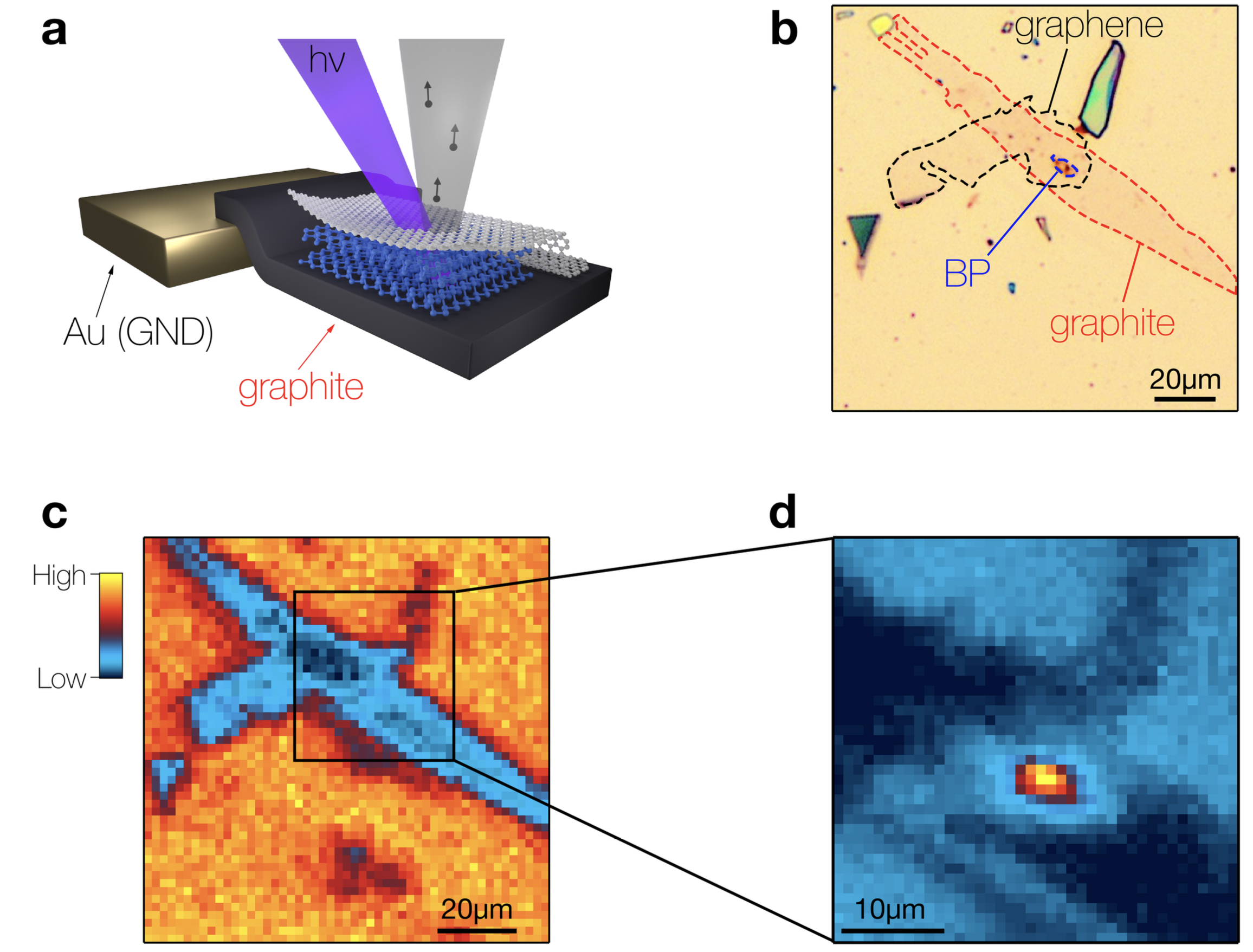
Figure 1 illustrates the methodology used in our study. We prepare thin crystals of BP by micromechanical exfoliation and use a dry-transfer technique to encapsulate the BP flakes between a graphite bottom electrode and ML graphene. All heterostructures were prepared under protective atmosphere and supported on Au coated Si/SiO2 substrates. More details of the sample preparation are given in Supporting Information, section I. To study the thickness dependence of the electronic structure, we prepared and measured more than a dozen heterostructures.
Typical few-layer BP flakes have lateral dimensions of the order of 10 m, far below what is needed for conventional ARPES experiments. To enable electronic structure studies on samples of these dimensions, we developed an instrument that combines the high energy and momentum resolution of laser-ARPES with a spatial resolution below 2 m. This is achieved by focusing a 6 eV continuous wave laser (LEOS solutions) with an aberration corrected lens mounted in ultra-high vacuum [36]. The encapsulated BP flakes are then localized by raster scanning the samples under the focused beam while recording the photocurrent near normal emission in an energy range of a few hundred meV below the Fermi level. In this energy-momentum range, direct transitions are forbidden in graphene and graphite. These materials thus appear as strong depressions in the photocurrent maps, which allows for a convenient correlation with optical micrographs, as illustrated in Figure 1b,c. Finally, we identify the BP flake by mapping the photocurrent for an orientation of the linear polarization where BP has a strong photoemission intensity (Figure 1d).
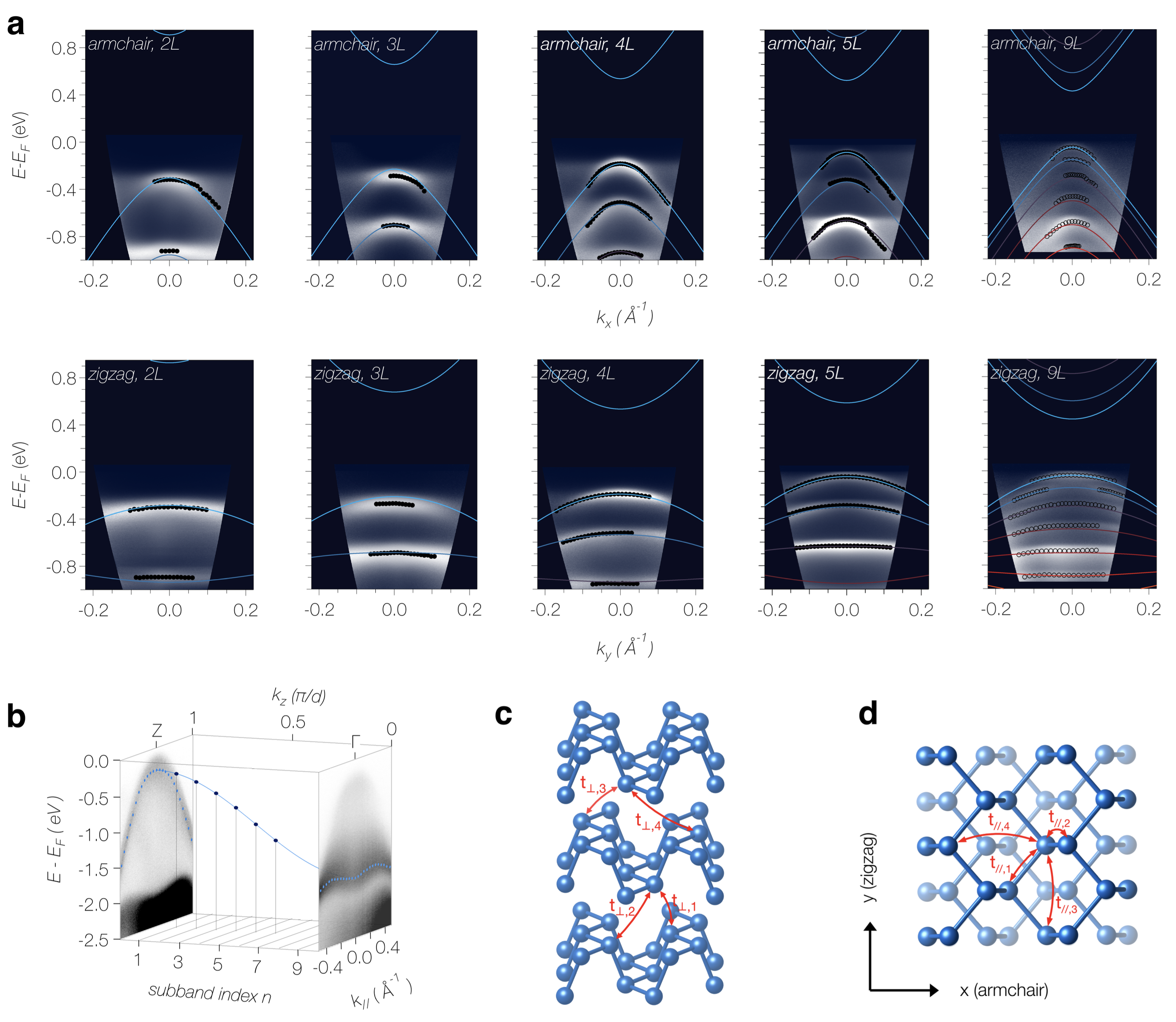
Figure 2a shows laser -ARPES data from a set of encapsulated BP flakes with layers thickness. The data clearly resolve a series of distinct subbands in the energy range eV probed in our experiments. The subband splitting decreases with increasing thickness, as expected for a quantum confined system. However, the subband energies deviate from the scaling with the square of the subband index observed in conventional semiconductor quantum wells. This is most evident in the data, where the subband splitting initially increases with but then appears to saturate. This behavior can be understood on a semi-quantitative level starting from a phenomenological quantization condition where is the number of layers, their thickness and describes the leakage of the wave functions across the interface. Since bulk BP has the VBM at the zone boundary , it is convenient to write the quantization of the perpendicular momentum as so that the subband defines the VBM. Using a simple cosine dispersion along – which is known to be a good approximation to the bulk band structure of BP [37] – this model shows excellent agreement with the measured quantum well energies of BP for and the independently measured bulk bandwidth along Z of 1.35 eV (see Figure 2b). Hence, the above quantization condition provides a simple explanation of a key aspect of the electronic structure. At the same time it serves as a reliable cross-check of the thickness of individual samples (see Supporting Information, Figure S3). Describing the conduction band in an analogous way proved to give a good parametrization of the optical gap of BP [7]. However, such models are not suitable for describing the full quasiparticle dispersion.
BP has a strong structural anisotropy arising from a puckering of the honeycomb lattice of individual layers. DFT studies predicted that this results in a strong and thickness dependent electronic anisotropy. Our data in Figure 2 directly confirm a significant electronic anisotropy. Along the zigzag direction, we find a parabolic band with heavy in-plane mass, while the dispersion in the orthogonal armchair direction is stronger and crosses over from parabolic at low energy to nearly linear at high energy. This dichotomy in the character of holes moving along orthogonal directions can be seen as a remnant of the topological Dirac semimetal state predicted at very high electric field [38] and reported in surface-doped bulk BP [39]. A careful examination of the data also reveals faint non-dispersive spectral features just below the top of each subband. We will characterize and discuss these features in Figure 4.
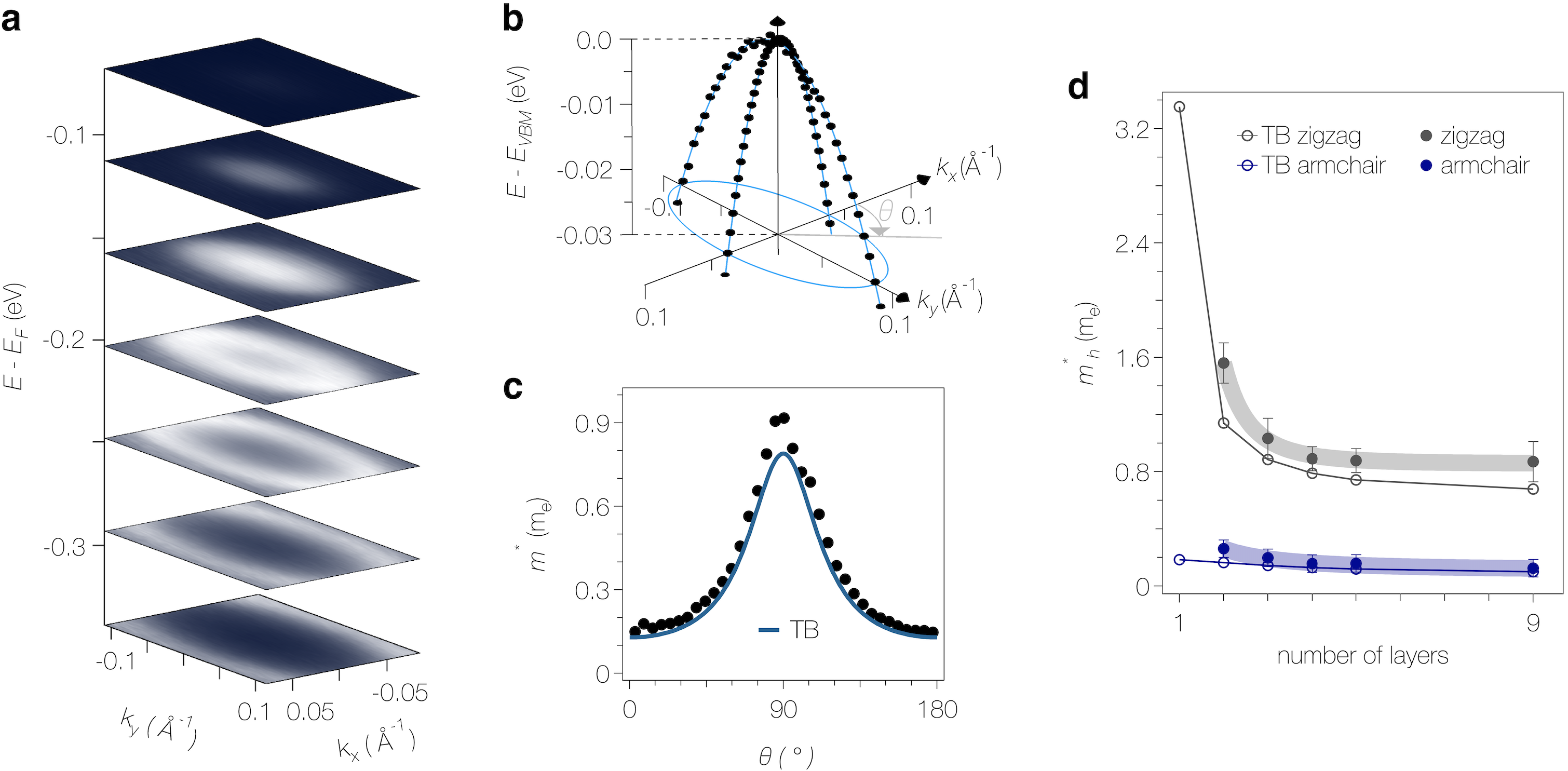
First, we quantify effective masses. Directional effective band masses are of pivotal importance in semiconductor physics but have thus far remained inaccessible to experiment in few-layer BP. Figure 3a shows a series of constant energy contours of BP extracted from a full 3D data set. One can clearly recognize elliptical contours over an extended energy range, which is characteristic for an anisotropic two-dimensional electron gas (2DEG) characterized by two effective masses only. The low-energy band dispersion along both high-symmetry directions (Figure 3b) directly confirms a highly parabolic nature of the subband over an energy range of meV, corresponding to carrier densities up to cm-2, comparable to the density range accessible with electrostatic gating using hexagonal boron nitride dielectrics. This rationalizes the linear Landau-level splitting reported in Ref [28]. The effective masses in BP are and me for the armchair and zigzag direction, respectively. This corresponds to a cyclotron mass me, slightly higher than the range of me reported in quantum oscillation studies of the charge accumulation layer in gated BP [40, 41, 25, 23, 42, 28]. From the above masses of BP we obtain an anisotropy , which is lower than found in most DFT calculations [5, 8] but is well reproduced by our tight-binding model (Figure 3c). Extending the analysis of effective masses to other devices reveals a systematic trend to higher effective masses as the thickness is reduced (Figure 3c,d). This trend is comparable along both high symmetry directions leaving the electronic anisotropy nearly constant.
We now introduce a quantitative tight-binding description of the full experimental quasiparticle dispersion in few-layer BP. BP has a complex electronic structure with the 5 valence electrons of phosphorus distributed over all 4 orbitals [29, 30, 31, 6]. However, theoretical studies found that the ab initio band structure of few-layer BP near the VBM is well captured by an effective single orbital tight-binding model [30, 31, 32]. In the following, we determine the parameters of this model directly from experiment. We start our quantitative analysis by extracting band dispersions from a curvature analysis of the experimental data (black circles in Figure 2a) [43]. Studying different parametrizations of the experimental band structure extracted in this way, we find that a minimal model with only 2 in-plane and 1 out-of-plane parameters is insufficient to simultaneously capture the experimentally observed subband splittings and masses. A good description of the data is obtained by restricting the tight-binding model of Refs. [31, 32] to the 4 in-plane and 4 out-of-plane parameters indicated in Figure 2c,d. We find that including the additional 6 parameters used in these theoretical works does not improve the fit of our experimental data significantly.
| intralayer (eV) | interlayer (eV) | ||
For a robust analysis, we fit the eigenvalues of the 8-parameter tight-binding model simultaneously to the band dispersions along both high-symmetry directions of all observed quantum well states of the , , and data and additionally restrict the fit to reproduce the bulk band gap. This results in the single set of parameters shown in Table 1. In Figure 2a, the bands calculated with this set of parameters are overlaid on the experimental data. We find good agreement with all subband energies as well as the thickness and subband dependent dispersions. Additionally, our tight-binding model also reproduces the thickness dependence of the optical band gap reported in the literature (Supporting Information, Figure S2) [7, 8, 9, 10]. As a further test of the model, we calculate the subband dispersions for BP (not included in the fitting procedure) and overlay them on the data in Figure 2a. The good agreement implies that our parametrization provides an accurate description of a wide range of thickness.
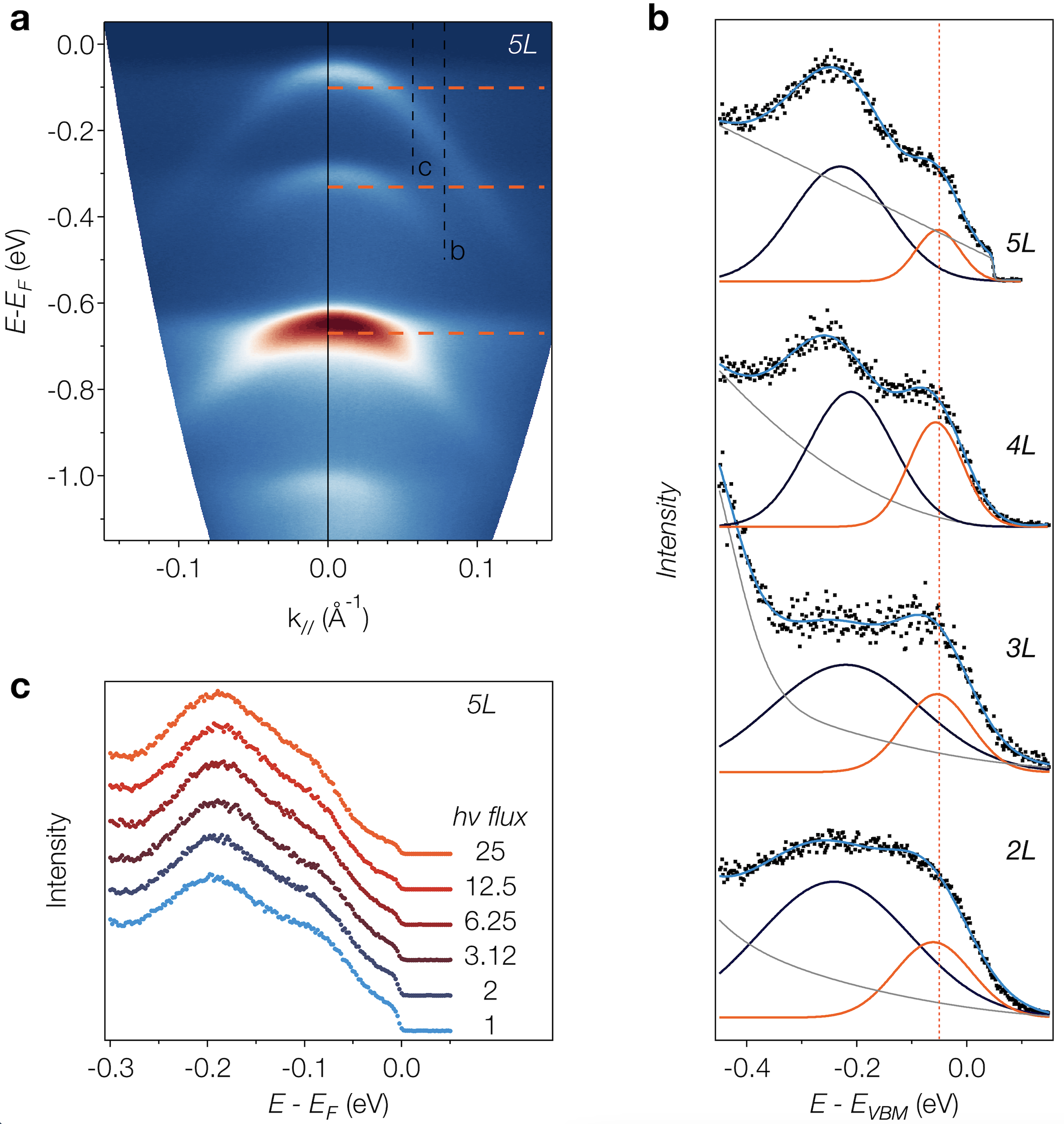
We now discuss the dispersionless spectral signatures discernible along the armchair direction. These features (marked by orange lines in Figure 4a) are ubiquitous in our data. They are present in all devices and are systematically located meV below the top of each subband. Understanding their origin and contribution to the properties of BP represents a challenge with potential implications for other 2D materials.
An interesting possibility is that these features arise from interface effects. The interface of BP with the graphene encapsulation used in this work forms a periodic moiré pattern. Scanning tunnelling microscopy showed that this causes the formation of Landau levels in graphene associated with the strain-induced pseudo magnetic field [44]. Such Landau levels are intrinsically non-dispersive. However, their energy scaling and sensitivity to the twist angle [44] – which is uncontrolled in our study and thus inevitably different from device to device – is inconsistent with our observations. Flat bands can also arise from a superlattice potential in the active layer and have been detected by ARPES in multiple moiré systems [45, 46, 47, 48]. However, the systematic pinning of the dispersionless features at the same energy relative to a subband, irrespective of the twist angle of an individual device, is difficult to reconcile with moiré physics.
We note that a recent time-resolved photoemission study on bulk BP reported Floquet bands with similarities to the dispersionless features in our data [49]. Given the high photon flux density in our measurements ( s-1 focused in a spot of m2), one cannot a priori exclude light induced effects on the electronic spectrum. This also includes the creation and probing of a steady-state exciton population [50]. However, Figure 4c shows that the 2-peak structure arising from the dispersionless features is unaffected if the photon flux is varied by more than an order of magnitude. This excludes Floquet bands [49] or a dynamic exciton population [50] as the origin of the relevant spectral features.
The 2-peak structure arising from the non-dispersive features also resembles the spectral function of a filled band with strong electron-phonon coupling [51, 52]. Moreover, the energy of meV observed experimentally is close to the frequency of optical phonons in BP [53, 54]. On the other hand, the high room-temperature mobility of BP indicates that the electron-phonon coupling strength in BP is modest. Simple model calculations for weak to moderate coupling reproduce a dispersionless spectral feature at the right energy but predict that its spectral weight is weak and decays more rapidly away from the main band than observed experimentally (see Supporting Information, section VI).
Interestingly, a recent theoretical study predicts a strong temperature dependence of electron-phonon coupling in BP, raising the possibility of self-trapped small polarons at low-temperature which delocalize at higher temperature [54]. This might reconcile a high room-temperature mobility with strong electron phonon coupling effects at low temperature. It would be interesting to address this possibility in future temperature-dependent -ARPES experiments. Varying the carrier density by electrostatic gating may provide another route to controlling electron-phonon coupling [55, 56].
In conclusion, we reported a comprehensive study of the quasiparticle dispersion in few-layer BP. Our data directly resolve a multitude of anisotropic quantum well states. We quantify their dispersion and determine universal tight-binding parameters which provide an accurate description of the full electronic structure over a range of thickness. This provides a solid foundation for the interpretation of complementary experiments on BP devices. We further reported novel dispersionless spectral features which may be relevant for the physical properties of BP.
I Acknowledgments
We thank Alex Ferreira for the development of the dry transfer system. This work was primarily supported through the Swiss National Science Foundation (SNSF) Div. II. I.G.-L. and A.F.M acknowledge support from the EU graphene flagship. S.P. acknowledges support from the F.R.S.-FNRS as well as from the EU Horizon 2020 Research and Innovation Programme, under the Marie Sklodowska-Curie Grant Agreement SELPH2D No. 839217 and the PRACE-21 resources MareNostrum at BSC-CNS. M.G. acknowledges support from the Italian Ministry for University and Research through the Levi-Montalcini program.
References
- Li et al. [2014] L. Li, Y. Yu, G. J. Ye, Q. Ge, X. Ou, H. Wu, D. Feng, X. H. Chen, and Y. Zhang, Black phosphorus field-effect transistors, Nature Nanotechnology 9, 372 (2014).
- Youngblood et al. [2015] N. Youngblood, C. Chen, S. J. Koester, and M. Li, Waveguide-integrated black phosphorus photodetector with high responsivity and low dark current, Nature Photonics 9, 247 (2015).
- Kim et al. [2021] H. Kim, S. Z. Uddin, D.-H. Lien, M. Yeh, N. S. Azar, S. Balendhran, T. Kim, N. Gupta, Y. Rho, C. P. Grigoropoulos, K. B. Crozier, and A. Javey, Actively variable-spectrum optoelectronics with black phosphorus, Nature 596, 232 (2021).
- Carvalho et al. [2016] A. Carvalho, M. Wang, X. Zhu, A. S. Rodin, H. Su, and A. H. Castro Neto, Phosphorene: From theory to applications, Nature Reviews Materials 1, 10.1038/natrevmats.2016.61 (2016).
- Tran et al. [2014] V. Tran, R. Soklaski, Y. Liang, and L. Yang, Layer-controlled band gap and anisotropic excitons in few-layer black phosphorus, Physical Review B 89, 235319 (2014).
- Qiao et al. [2014] J. Qiao, X. Kong, Z. X. Hu, F. Yang, and W. Ji, High-mobility transport anisotropy and linear dichroism in few-layer black phosphorus, Nature Communications 5, 4475 (2014).
- Li et al. [2017] L. Li, J. Kim, C. Jin, G. J. Ye, D. Y. Qiu, F. H. Da Jornada, Z. Shi, L. Chen, Z. Zhang, F. Yang, K. Watanabe, T. Taniguchi, W. Ren, S. G. Louie, X. H. Chen, Y. Zhang, and F. Wang, Direct observation of the layer-dependent electronic structure in phosphorene, Nature Nanotechnology 12, 21 (2017).
- Yang et al. [2015] J. Yang, R. Xu, J. Pei, Y. W. Myint, F. Wang, Z. Wang, S. Zhang, Z. Yu, and Y. Lu, Optical tuning of exciton and trion emissions in monolayer phosphorene, Light: Science and Applications 4, e312 (2015).
- Zhang et al. [2017a] G. Zhang, S. Huang, A. Chaves, C. Song, V. O. Özçelik, T. Low, and H. Yan, Infrared fingerprints of few-layer black phosphorus, Nature Communications 8, 14071 (2017a).
- Zhang et al. [2018] G. Zhang, A. Chaves, S. Huang, F. Wang, Q. Xing, T. Low, and H. Yan, Determination of layer-dependent exciton binding energies in few-layer black phosphorus, Science Advances 4, eaap9977 (2018).
- Wang et al. [2015] X. Wang, A. M. Jones, K. L. Seyler, V. Tran, Y. Jia, H. Zhao, H. Wang, L. Yang, X. Xu, and F. Xia, Highly anisotropic and robust excitons in monolayer black phosphorus, Nature Nanotechnology 10, 517 (2015).
- Wang et al. [2020] J. Wang, A. Rousseau, M. Yang, T. Low, S. Francoeur, and S. Kéna-Cohen, Mid-infrared polarized emission from black phosphorus light-emitting diodes, Nano Letters 20, 3651 (2020).
- Rodin et al. [2014] A. S. Rodin, A. Carvalho, and A. H. Castro Neto, Strain-induced gap modification in black phosphorus, Physical Review Letters 112, 1 (2014), arXiv:1401.1801 .
- Zhang et al. [2017b] Z. Zhang, L. Li, J. Horng, N. Z. Wang, F. Yang, Y. Yu, Y. Zhang, G. Chen, K. Watanabe, T. Taniguchi, X. H. Chen, F. Wang, and Y. Zhang, Strain-Modulated Bandgap and Piezo-Resistive Effect in Black Phosphorus Field-Effect Transistors, Nano Letters 17, 6097 (2017b).
- Deng et al. [2017] B. Deng, V. Tran, Y. Xie, H. Jiang, C. Li, Q. Guo, X. Wang, H. Tian, S. J. Koester, H. Wang, J. J. Cha, Q. Xia, L. Yang, and F. Xia, Efficient electrical control of thin-film black phosphorus bandgap, Nature Communications 8, 4 (2017).
- Liu et al. [2017] Y. Liu, Z. Qiu, A. Carvalho, Y. Bao, H. Xu, S. J. Tan, W. Liu, A. H. Castro Neto, K. P. Loh, and J. Lu, Gate-Tunable Giant Stark Effect in Few-Layer Black Phosphorus, Nano Letters 17, 1970 (2017).
- Sherrott et al. [2019] M. C. Sherrott, W. S. Whitney, D. Jariwala, S. Biswas, C. M. Went, J. Wong, G. R. Rossman, and H. A. Atwater, Anisotropic Quantum Well Electro-Optics in Few-Layer Black Phosphorus, Nano Letters 19, 269 (2019).
- Chen et al. [2020] C. Chen, X. Lu, B. Deng, X. Chen, Q. Guo, C. Li, C. Ma, S. Yuan, E. Sung, K. Watanabe, T. Taniguchi, L. Yang, and F. Xia, Widely tunable mid-infrared light emission in thin-film black phosphorus, Science Advances 6, eaay6134 (2020).
- Zhang et al. [2020] Y. Zhang, S. Wang, S. Chen, Q. Zhang, X. Wang, X. Zhu, X. Zhang, X. Xu, T. Yang, M. He, X. Yang, Z. Li, X. Chen, M. Wu, Y. Lu, R. Ma, W. Lu, and A. Pan, Wavelength-Tunable Mid-Infrared Lasing from Black Phosphorus Nanosheets, Advanced Materials 32, 1 (2020).
- Peng et al. [2017] R. Peng, K. Khaliji, N. Youngblood, R. Grassi, T. Low, and M. Li, Midinfrared electro-optic modulation in few-layer black phosphorus, Nano Letters 17, 6315 (2017).
- Island et al. [2015] J. O. Island, G. A. Steele, H. S. Van Der Zant, and A. Castellanos-Gomez, Environmental instability of few-layer black phosphorus, 2D Materials 2, 10.1088/2053-1583/2/1/011002 (2015), arXiv:1410.2608 .
- Wang et al. [2016a] G. Wang, W. J. Slough, R. Pandey, and S. P. Karna, Degradation of phosphorene in air: Understanding at atomic level, 2D Materials 3, 10.1088/2053-1583/3/2/025011 (2016a).
- Cao et al. [2015] Y. Cao, A. Mishchenko, G. L. Yu, E. Khestanova, A. P. Rooney, E. Prestat, A. V. Kretinin, P. Blake, M. B. Shalom, C. Woods, J. Chapman, G. Balakrishnan, I. V. Grigorieva, K. S. Novoselov, B. A. Piot, M. Potemski, K. Watanabe, T. Taniguchi, S. J. Haigh, A. K. Geim, and R. V. Gorbachev, Quality Heterostructures from Two-Dimensional Crystals Unstable in Air by Their Assembly in Inert Atmosphere, Nano Letters 15, 4914 (2015).
- Abate et al. [2018] Y. Abate, D. Akinwande, S. Gamage, H. Wang, M. Snure, N. Poudel, and S. B. Cronin, Recent Progress on Stability and Passivation of Black Phosphorus, Advanced Materials 30, 1 (2018).
- Chen et al. [2015] X. Chen, Y. Wu, Z. Wu, Y. Han, S. Xu, L. Wang, W. Ye, T. Han, Y. He, Y. Cai, and N. Wang, High-quality sandwiched black phosphorus heterostructure and its quantum oscillations, Nature Communications 6, 7315 (2015).
- Long et al. [2016] G. Long, D. Maryenko, J. Shen, S. Xu, J. Hou, Z. Wu, W. K. Wong, T. Han, J. Lin, Y. Cai, R. Lortz, and N. Wang, Achieving Ultrahigh Carrier Mobility in Two-Dimensional Hole Gas of Black Phosphorus, Nano Letters 16, 7768 (2016).
- Li et al. [2016] L. Li, F. Yang, G. J. Ye, Z. Zhang, Z. Zhu, W. Lou, X. Zhou, L. Li, K. Watanabe, T. Taniguchi, K. Chang, Y. Wang, X. H. Chen, and Y. Zhang, Quantum Hall effect in black phosphorus two-dimensional electron system, Nature Nanotechnology 11, 593 (2016).
- Yang et al. [2018] J. Yang, S. Tran, J. Wu, S. Che, P. Stepanov, T. Taniguchi, K. Watanabe, H. Baek, D. Smirnov, R. Chen, and C. N. Lau, Integer and Fractional Quantum Hall effect in Ultrahigh Quality Few-layer Black Phosphorus Transistors, Nano Letters 18, 229 (2018).
- Morita [1986] A. Morita, Semiconducting black phosphorus, Applied Physics A Solids and Surfaces 39, 227 (1986).
- Rudenko and Katsnelson [2014] A. N. Rudenko and M. I. Katsnelson, Quasiparticle band structure and tight-binding model for single- and bilayer black phosphorus, Physical Review B - Condensed Matter and Materials Physics 89, 1 (2014), arXiv:1404.0618 .
- Rudenko et al. [2015] A. N. Rudenko, S. Yuan, and M. I. Katsnelson, Toward a realistic description of multilayer black phosphorus: From GW approximation to large-scale tight-binding simulations, Physical Review B 92, 085419 (2015).
- De Sousa et al. [2017] D. J. De Sousa, L. V. De Castro, D. R. Da Costa, J. M. Pereira, and T. Low, Multilayered black phosphorus: From a tight-binding to a continuum description, Physical Review B 96, 155427 (2017).
- Low et al. [2014] T. Low, A. S. Rodin, A. Carvalho, Y. Jiang, H. Wang, F. Xia, and A. H. Castro Neto, Tunable optical properties of multilayer black phosphorus thin films, Physical Review B 90, 3 (2014).
- Cai et al. [2014] Y. Cai, G. Zhang, and Y. W. Zhang, Layer-dependent band alignment and work function of few-layer phosphorene, Scientific Reports 4, 1 (2014).
- Castellanos-Gomez et al. [2014] A. Castellanos-Gomez, L. Vicarelli, E. Prada, J. O. Island, K. L. Narasimha-Acharya, S. I. Blanter, D. J. Groenendijk, M. Buscema, G. A. Steele, J. V. Alvarez, H. W. Zandbergen, J. J. Palacios, and H. S. Van Der Zant, Isolation and characterization of few-layer black phosphorus, 2D Materials 1, 0 (2014).
- Cucchi et al. [2019] I. Cucchi, I. Gutiérrez-Lezama, E. Cappelli, S. M. K. Walker, F. Y. Bruno, G. Tenasini, L. Wang, N. Ubrig, C. Barreteau, E. Giannini, M. Gibertini, A. Tamai, A. F. Morpurgo, and F. Baumberger, Microfocus Laser-Angle-Resolved Photoemission on Encapsulated Mono-, Bi-, and Few-Layer 1T’-WTe2, Nano Letters 19, 554 (2019).
- Ehlen et al. [2016] N. Ehlen, B. V. Senkovskiy, A. V. Fedorov, A. Perucchi, P. Di Pietro, A. Sanna, G. Profeta, L. Petaccia, and A. Grüneis, Evolution of electronic structure of few-layer phosphorene from angle-resolved photoemission spectroscopy of black phosphorous, Phys. Rev. B 94, 245410 (2016).
- Liu et al. [2015] Q. Liu, X. Zhang, L. B. Abdalla, A. Fazzio, and A. Zunger, Switching a normal insulator into a topological insulator via electric field with application to phosphorene, Nano Letters 15, 1222 (2015).
- Kim et al. [2015] J. Kim, S. S. Baik, S. H. Ryu, Y. Sohn, S. Park, B.-G. Park, J. Denlinger, Y. Yi, H. J. Choi, and K. S. Kim, Observation of tunable band gap and anisotropic dirac semimetal state in black phosphorus, Science 349, 723 (2015).
- Gillgren et al. [2015] N. Gillgren, D. Wickramaratne, Y. Shi, T. Espiritu, J. Yang, J. Hu, J. Wei, X. Liu, Z. Mao, K. Watanabe, T. Taniguchi, M. Bockrath, Y. Barlas, R. K. Lake, and C. N. Lau, Gate tunable quantum oscillations in air-stable and high mobility few-layer phosphorene heterostructures, 2D Materials 2, 011001 (2015).
- Li et al. [2015] L. Li, G. J. Ye, V. Tran, R. Fei, G. Chen, H. Wang, J. Wang, K. Watanabe, T. Taniguchi, L. Yang, X. H. Chen, and Y. Zhang, Quantum oscillations in a two-dimensional electron gas in black phosphorus thin films, Nature Nanotechnology 10, 608 (2015).
- Tayari et al. [2015] V. Tayari, N. Hemsworth, I. Fakih, A. Favron, E. Gaufrès, G. Gervais, R. Martel, and T. Szkopek, Two-dimensional magnetotransport in a black phosphorus naked quantum well, Nature Communications 6, 7702 (2015).
- Zhang et al. [2011] P. Zhang, P. Richard, T. Qian, Y.-M. Xu, X. Dai, and H. Ding, A precise method for visualizing dispersive features in image plots, Review of Scientific Instruments 82, 043712 (2011).
- Liu et al. [2018] Y. Liu, J. N. B. Rodrigues, Y. Z. Luo, L. Li, A. Carvalho, M. Yang, E. Laksono, J. Lu, Y. Bao, H. Xu, S. J. R. Tan, Z. Qiu, C. H. Sow, Y. P. Feng, A. H. C. Neto, S. Adam, J. Lu, and K. P. Loh, Tailoring sample-wide pseudo-magnetic fields on a graphene–black phosphorus heterostructure, Nature Nanotechnology 13, 828 (2018).
- Utama et al. [2021] M. I. B. Utama, R. J. Koch, K. Lee, N. Leconte, H. Li, S. Zhao, L. Jiang, J. Zhu, K. Watanabe, T. Taniguchi, P. D. Ashby, A. Weber-Bargioni, A. Zettl, C. Jozwiak, J. Jung, E. Rotenberg, A. Bostwick, and F. Wang, Visualization of the flat electronic band in twisted bilayer graphene near the magic angle twist, Nature Physics 17, 184 (2021).
- Lisi et al. [2021] S. Lisi, X. Lu, T. Benschop, T. A. de Jong, P. Stepanov, J. R. Duran, F. Margot, I. Cucchi, E. Cappelli, A. Hunter, A. Tamai, V. Kandyba, A. Giampietri, A. Barinov, J. Jobst, V. Stalman, M. Leeuwenhoek, K. Watanabe, T. Taniguchi, L. Rademaker, S. J. van der Molen, M. P. Allan, D. K. Efetov, and F. Baumberger, Observation of flat bands in twisted bilayer graphene, Nature Physics 17, 189 (2021).
- Stansbury et al. [2021] C. H. Stansbury, M. I. B. Utama, C. G. Fatuzzo, E. C. Regan, D. Wang, Z. Xiang, M. Ding, K. Watanabe, T. Taniguchi, M. Blei, Y. Shen, S. Lorcy, A. Bostwick, C. Jozwiak, R. Koch, S. Tongay, J. Avila, E. Rotenberg, F. Wang, and A. Lanzara, Visualizing electron localization of WS2/WSe2 moiré superlattices in momentum space, Science Advances 7, eabf4387 (2021).
- Gatti et al. [2022] G. Gatti, J. Issing, L. Rademaker, F. Margot, T. A. de Jong, S. J. van der Molen, J. Teyssier, T. K. Kim, M. D. Watson, C. Cacho, P. Dudin, J. Avila, K. C. Edwards, P. Paruch, N. Ubrig, I. Gutiérrez-Lezama, A. Morpurgo, A. Tamai, and F. Baumberger, Observation of flat moiré bands in twisted bilayer WSe2 (2022), arXiv:2211.01192 [cond-mat.str-el] .
- Zhou et al. [2023] S. Zhou, C. Bao, B. Fan, H. Zhou, Q. Gao, H. Zhong, T. Lin, H. Liu, P. Yu, P. Tang, S. Meng, W. Duan, and S. Zhou, Pseudospin-selective floquet band engineering in black phosphorus, Nature 614, 75 (2023).
- Weinelt et al. [2004] M. Weinelt, M. Kutschera, T. Fauster, and M. Rohlfing, Dynamics of exciton formation at the si(100) surface, Phys. Rev. Lett. 92, 126801 (2004).
- Goodvin and Berciu [2008] G. L. Goodvin and M. Berciu, Momentum average approximation for models with electron-phonon coupling dependent on the phonon momentum, Phys. Rev. B 78, 235120 (2008).
- Mazzola et al. [2013] F. Mazzola, J. W. Wells, R. Yakimova, S. Ulstrup, J. A. Miwa, R. Balog, M. Bianchi, M. Leandersson, J. Adell, P. Hofmann, and T. Balasubramanian, Kinks in the band of graphene induced by electron-phonon coupling, Phys. Rev. Lett. 111, 216806 (2013).
- Sohier et al. [2018] T. Sohier, D. Campi, N. Marzari, and M. Gibertini, Mobility of two-dimensional materials from first principles in an accurate and automated framework, Phys. Rev. Materials 2, 114010 (2018).
- Neverov et al. [2021] V. D. Neverov, A. E. Lukyanov, Y. V. Zhumagulov, A. V. Krasavin, and V. Perebeinos, Polaronic signatures in pristine phosphorene, Phys. Rev. Mater. 5, 054008 (2021).
- Wang et al. [2016b] Z. Wang, S. McKeown Walker, A. Tamai, Y. Wang, Z. Ristic, F. Y. Bruno, A. de la Torre, S. Riccò, N. C. Plumb, M. Shi, P. Hlawenka, J. Sánchez-Barriga, A. Varykhalov, T. K. Kim, M. Hoesch, P. D. C. King, W. Meevasana, U. Diebold, J. Mesot, B. Moritz, T. P. Devereaux, M. Radovic, and F. Baumberger, Tailoring the nature and strength of electron–phonon interactions in the SrTiO3(001) 2D electron liquid, Nature Materials 15, 835 (2016b).
- Nguyen et al. [2019] P. V. Nguyen, N. C. Teutsch, N. P. Wilson, J. Kahn, X. Xia, A. J. Graham, V. Kandyba, A. Giampietri, A. Barinov, G. C. Constantinescu, N. Yeung, N. D. Hine, X. Xu, D. H. Cobden, and N. R. Wilson, Visualizing electrostatic gating effects in two-dimensional heterostructures, Nature 572, 220 (2019).