tcb@breakable
NicePIM: Design Space Exploration for Processing-In-Memory DNN Accelerators with 3D-Stacked-DRAM
Abstract
With the widespread use of deep neural networks(DNNs) in intelligent systems, DNN accelerators with high performance and energy efficiency are greatly demanded. As one of the feasible processing-in-memory(PIM) architectures, 3D-stacked-DRAM-based PIM(DRAM-PIM) architecture enables large-capacity memory and low-cost memory access, which is a promising solution for DNN accelerators with better performance and energy efficiency. However, the low-cost characteristics of stacked DRAM and the distributed manner of memory access and data storing require us to rebalance the hardware design and DNN mapping. In this paper, we propose NicePIM to efficiently explore the design space of hardware architecture and DNN mapping of DRAM-PIM accelerators, which consists of three key components: PIM-Tuner, PIM-Mapper and Data-Scheduler. PIM-Tuner optimizes the hardware configurations leveraging a DNN model for classifying area-compliant architectures and a deep kernel learning model for identifying better hardware parameters. PIM-Mapper explores a variety of DNN mapping configurations, including parallelism between branches of DNN, DNN layer partitioning, DRAM capacity allocation and data layout pattern in DRAM to generate high-hardware-utilization DNN mapping schemes for various hardware configurations. The Data-Scheduler employs an integer-linear-programming-based data scheduling algorithm to alleviate the inter-PIM-node communication overhead of data-sharing brought by DNN layer partitioning. Experimental results demonstrate that NicePIM can optimize hardware configurations for DRAM-PIM systems effectively and can generate high-quality DNN mapping schemes with latency and energy cost reduced by 37% and 28% on average respectively compared to the baseline method.
Index Terms:
Processing-in-memory, DNN accelerator, design space exploration.I Introduction
Deep neural networks(DNNs) have been used in many fields including image recognition, object detection and natural language processing, showing unprecedented accuracy. The majority of operations in DNNs are multiply-accumulate(MAC) operations with a large amount of data reuse, which makes DNNs compute-intensive and memory-intensive. With the scale of DNNs increasingly growing, the acceleration becomes a critical issue in the application of DNNs. Many domain-specific DNN accelerators have been proposed to get improved performance and energy efficiency[1, 2, 3, 4, 5]. Due to the large memory footprint of DNNs, one of the major concerns of these DNN accelerators is the costly off-chip DRAM access. The memory hierarchy of DNN accelerators is elaborately designed to reduce off-chip DRAM access. A large part of the area of the chip is spent on buffers to make data more reused on chip. Elaborate scheduling strategies are often employed to make sufficient use of the capacity of the on-chip memory[6, 7, 8].
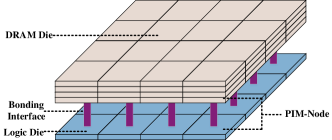
The technology of 3D-stacked memories enables the integration of large-capacity memory with low access cost[9, 10, 11], which provides a promising solution to the memory wall problem[12]. In systems with 3D-stacked memory, the stacked logic die has the same area as the memory die and they are integrated by 3D-stacking technologies such as through silicon via(TSV)[9], hybrid bonding[10], etc. Among the widely used memory technologies, DRAM has relatively high density, so 3D-stacked-DRAM-based processing-in-memory system(DRAM-PIM system) is one of the promising choices for systems with high memory bandwidth and energy efficiency. The DRAM die contains an array of DRAM banks[10](or vaults[9]) and each DRAM bank can be accessed independently in parallel instead of through the standard DDR interface. The 3D integration technology enables the stacked DRAM to have an order of magnitude higher bandwidth compared to conventional off-chip DRAM, and the closer distance between the memory and the logic makes the energy efficiency more than 5x better than off-chip DRAM[10]. 3D-stacked DRAM has been used in many systems for the acceleration of memory-intensive applications [13, 14, 15]. Due to the array-architecture of the DRAM, typically, as shown in Figure 1, the logic die is divided into an array and each part is combined with the corresponding DRAM bank(s) to form a function unit, which is denoted as a PIM-node. In each PIM-node, the logic part has independent access to the counterpart DRAM but each PIM-node has no direct access to the DRAM of other PIM-nodes. PIM-nodes communicate with each other through the on-chip-interconnect in the logic die such as network-on-chip(NoC). This distributed manner of computation and data storing benefits the utilization of the DRAM bandwidth of the DRAM-PIM system, but requires rebalancing the architecture design and the mapping algorithm.
Recently proposed DRAM-PIM-based DNN accelerators are typically organized into a homogeneous tiled architecture[13, 16, 17, 18, 19], which is in coordination with the array architecture of 3D-stacked DRAM. Each PIM-node can do DNN computation independently and the NN engine in each PIM-node contains SRAM buffers and a processing-element(PE) array which can do MAC operations. The aforementioned works mainly focus on the architecture design and scheduling within one PIM-node, and they use simple DNN mapping strategies, paying little attention to the overhead brought by the distributed manner of computation and data storing. Besides, these works are customized designs for their workloads and targets, and may require manual tuning if the hardware constraints or the design target change.
To meet the requirements of different targets under different hardware constraints, design space exploration(DSE) methods that generate high-quality hardware configurations and DNN mappings are necessary.
The diverse choices of software mapping and hardware architecture of DRAM-PIM accelerators lead to a huge design space, making it impossible to find the optimal architecture by exhaustive search. In this work, given the configuration of the stacked DRAM with a certain number of DRAM banks and area, the following design space of DRAM-PIM accelerators is considered:
For hardware configuration, the granularity of PIM-nodes, PE array size and buffer sizes are taken into account:
(1) For a DRAM-PIM system with a certain number of DRAM banks, larger but fewer PIM-nodes have fewer inter-PIM-node communication requirements while more but smaller PIM-nodes enable more mapping flexibility. The number of allocated DRAM banks for one PIM-node determines its DRAM bandwidth, DRAM capacity and area.
(2)For one PIM-node with a certain number of allocated DRAM banks, the size of the PE array and sizes of SRAM buffers require a trade-off since a larger PE array increases the computing power and larger buffers allow more data reuse.
For DNN mapping, we consider the parallelism between branches of DNN, DNN layer partitioning, DRAM capacity allocation and data layout pattern in DRAM:
(1) Many popular DNNs have multi-branch architecture such as multi-head-attention in Transformers[20] and the inception block in GoogLeNet[21].
Making the branches processed in parallel rather than processing them serially on the PIM-node array can reduce the overhead brought by layer partitioning but may suffer from load imbalance between PIM-nodes.
(2) A DNN layer needs to be partitioned so that it can be processed in parallel on multiple PIM-nodes.
Different layer partition schemes correspond to different computation tasks of PIM-nodes and inter-PIM-node communication, which result in differences in performance.
(3) The width of DRAM banks is larger than the data width of data of DNNs, especially when a PIM-node has many DRAM banks, thus proper data layout pattern in DRAM is required to achieve full use of dram bandwidth.
(4) Due to the distributed manner of data storing, the DRAM of one PIM-node may not have enough capacity to store all weights of the whole DNN. If DRAM capacity is not sufficient for a PIM-node to store a whole replication of the weights of a layer, weights can be stored distributively and PIM-nodes share the weights when using. Sharing weights will require extra communication overhead while replicating the weights requires more DRAM capacity, so it is required to coordinate the weight replication values for all layers of the DNN.
Existing design space exploration methods for DNN accelerators[22, 23, 24, 25, 26] have diverse prior definitions on the architecture for effectively searching for DNN mapping and efficiently selecting hardware configuration, and thus are not suitable for DRAM-PIM architectures with the aforementioned design space. In this paper, we propose a framework named NicePIM to optimize the hardware design and DNN mapping of DRAM-PIM-based DNN accelerators, and the main contributions of this paper are as follows:
-
(1)
We propose NicePIM, a design space exploration framework for generating high-quality hardware design parameters and DNN mapping for DRAM-PIM-based DNN accelerators. NicePIM consists of a hardware design parameter optimizer(PIM-Tuner) that iteratively optimizes the hardware parameters and a DNN mapper(PIM-Mapper) with a Data-Scheduler to achieve high hardware utilization for various hardware configurations.
-
(2)
The PIM-Tuner searches for better hardware configurations that make proper use of the limited area of the logic die of the DRAM-PIM accelerator, taking the granularity of PIM-nodes, size of PE array and sizes of buffers into account. PIM-Tuner consists of a DNN model for classifying area-compliant architectures and a deep kernel learning model[27] for identifying hardware parameters with better quality.
-
(3)
The PIM-Mapper explores a variety of DNN mapping configurations, including parallelism between branches of the DNN, DNN layer partitioning, DRAM capacity allocation and data layout pattern in DRAM, for generating mapping schemes with high hardware utilization for various hardware configurations.
-
(4)
To reduce the inter-PIM-node communication overhead of data-sharing due to DNN layer partitioning, the Data-Scheduler builds an integer linear programming(ILP) model to schedule the data transfer process, trying to balance the load of NoC links.
-
(5)
Experimental results demonstrate that NicePIM can effectively optimize hardware configurations for DRAM-PIM systems and the proposed PIM-Mapper with the Data-Scheduler can reduce latency and energy cost by 37% and 28% on average respectively compared to the baseline method.
The remainder of this paper is organized as follows. Section II presents preliminaries about DRAM-PIM systems and DNNs. Section III introduces the defined design space. Section IV presents the overall flow of NicePIM with the following Section V, Section VI and Section VII introducing the details of the PIM-Tuner, PIM-Mapper and Data-Scheduler respectively. The experimental results are shown in Section VIII. Section IX lists some related works on 3D-stacked-memory-based PIM systems and design space exploration methods for DNN accelerators, followed by the conclusion in Section X.
II Preliminary
II-A PIM systems based on 3D-stacked DRAM
3D-stacked DRAM is a feasible solution for PIM systems with high performance and energy efficiency. We use the 3D-stacked DRAM from UnilC[10] as the substrate of the PIM system in this work. In this architecture, the DRAM banks in the DRAM die are organized into an array architecture. Each DRAM bank is connected to a controller in the corresponding part of the logic die and all controllers work independently. The function units of the DRAM-PIM system are placed in the remaining area of the logic die. Due to the array architecture of the DRAM banks, the function units in the logic die are divided into several parts and each part can directly access the DRAM bank(s) in the companion DRAM die. The function units and the corresponding DRAM bank(s) can be considered as an individual module denoted as a PIM-node. Each PIM-node accesses its own DRAM bank(s) with high speed and low cost but cannot directly access the DRAM banks of other PIM-nodes. We choose network-on-chip(NoC) as the on-chip-interconnect of the PIM-nodes for its feature of good extensibility and high-bandwidth.
II-B DNN fundamentals
A deep neural networks(DNN) consists of multiple layers to process data in a certain order. The first layer receives the input data and the output of each layer is forwarded to the following layers according to the network topology. Various kinds of layers are used in modern DNNs including convolution layer, matrix-multiplication layer(fully connected layer), pooling layer, normalization layer, etc. A DNN may contain multiple kinds of layers but in most DNNs, convolution layers and matrix-multiplication layers account for the dominant part of the computation [28, 29, 30, 21, 31, 32].
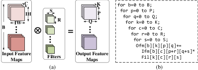
A convolution layer has a set of filters that slide on the input feature maps(ifmaps) to generate the output feature maps(ofmaps), which is shown in Figure 2-(a). During the sliding process, a window of , which is the same shape as the filter, is selected from the ifmaps and one point of the ofmap is generated after the dot-product of the selected window and the filter. For ifmaps of one sample in a batch, the sliding process of each filter is repeated for times. The computation process can be represented by the nested loops in Figure 2-(b). The feature maps generated by a convolution layer constitute a 4-D tensor, and we use , , , to represent its batch size, number of channels, height and width, respectively. Most convolution layers are followed by activation functions to add non-linearity to the ofmaps.
Matrix multiplication layers perform linear transformation for the inputs with the weight matrix. This kind of layer multiplies the input matrix of dimension with the weight matrix of dimension to generate the output matrix with dimension . Since the computation process can also be represented with the nested loops in Figure 2-(b) by setting the filter window size and ofmap size to , in this paper, we use the representations of convolution layers to represent matrix multiplication layers for simplicity, including the loop dimensions and data dimensions.
The topologies of DNNs are becoming more and more complicated. Most DNNs have linear structure and many popular DNNs have multi-branch architectures such as multi-head-attention in Transformers[20] and the inception block in GoogLeNet[21]. Many kinds of auxiliary layers are used to do down-sampling, concatenating, point-wise adding, point-wise multiplication, etc. These layers have simple computing processes and the number of operations is small so they are not major concerns in the design of DNN accelerators.
III Design Space Definition of the DRAM-PIM accelerator
This section introduces the considered design factors for the DRAM-PIM accelerator. The hardware architecture and the hardware design parameters are introduced in Section III-A. The following Section III-B, Section III-C, Section III-D and Section III-E introduce the DNN mapping configurations that should be considered for getting high hardware utilization on DRAM-PIM accelerators with various hardware parameters.
III-A Hardware configurations
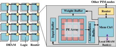
The hardware configuration mainly involves the granularity of PIM-nodes, PE array and buffers. As shown in Figure 3, the DRAM-PIM system is a homogeneous 2-D PIM-node array, which is a widely used structure in many 3D-stacking-memory-based PIM systems[13, 16, 18, 33]. A PIM-node consists of the stacked DRAM and the corresponding logic, and the logic part of the PIM-node has a NN engine, a DRAM bank controller and a router. PIM-nodes communicate with each other through the routers organized into mesh topology. A PIM-node can be allocated with one or several DRAM banks, and if a PIM-node has more than one DRAM bank, the ports of these DRAM banks are bound together so that the DRAM banks work in the same manner as one DRAM bank but with larger port-width. Besides, the total number of DRAM banks is constant so the number of allocated DRAM banks determines the number of PIM-nodes. The NN engine consists of a PE array and SRAM buffers for inputs, weights and outputs(and the partial-sums). The PE array is organized into parallel multiply-accumulation units, which is a widely used architecture [34, 35, 24].
The defined hardware design parameters are shown in Table I. We use the number of PIM-nodes to represent the granularity of PIM-nodes. The area, DRAM bandwidth and DRAM capacity of one PIM-node are proportional to the number of allocated DRAM banks. Larger but fewer PIM-nodes have fewer inter-PIM-node communication requirements since a DNN layer does not have to be partitioned into many parts to map on the PIM-node array. On the contrary, more but smaller PIM-nodes have more inter-PIM-node communication overhead, but enable more mapping flexibility. For a PIM-node with a certain number of allocated DRAM banks, a larger PE array enables larger computing power, and increasing the sizes of buffers allows more data reuse. However, too large PE arrays and buffer sizes make the area dissatisfy the constraint. We have the following constraints for the hardware configurations:
-
1)
The total area of the PIM-nodes should be no larger than the area of the DRAM die.
-
2)
and can exactly divide the rows and columns of the DRAM bank array to ensure homogeneous PIM-nodes.
| Parameters | Type | Comment | |
|---|---|---|---|
| Int | Number of rows of the PIM-node array | ||
| Int | Number of columns of the PIM-node array | ||
| Int | Number of rows of the PE array of a PIM-node | ||
| Int | Number of columns of the PE array of a PIM-node | ||
| Int | The input buffer size of a PIM-node | ||
| Int | The weight buffer size of a PIM-node | ||
| Int | The accumulation buffer size of a PIM-node |
III-B Parallelism between branches of DNN
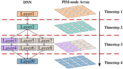
Since most DNNs have a linear structure and many popular DNNs have multi-branch architecture, we can make the branches processed on different regions of the PIM-node array to get inter-branch parallelism. We let the DRAM-PIM accelerator process the DNN in a timestep-by-timestep manner, which is shown in Figure 4. A DNN is partitioned into the smallest serial pieces possible and these parts of the DNN are denoted as segments. The total number of segments of a DNN is denoted as , which also means the DRAM-PIM accelerator requires timesteps to process them. If the -th segment has a multi-branch structure, the different branches can be processed in parallel and we denote the number of branches as . Layers in one branch are processed serially on the same region and for the -th branch, we denote the number of layers as . For example, in Figure 4, the of the 3-rd segment is 3 and all branches have 2 layers.
In the mapping process, we can make the branches processed with different parallelism. Making more branches processed in parallel on the PIM-node array can reduce the overhead brought by layer partitioning but may suffer from load imbalance between PIM-nodes. For the -th segment, the PIM-node array can be partitioned into at most regions and we use () to denote the number of regions. For the -th branch, it can be mapped onto a region of -th timestep and we denote the index of that region as (). For example, in Timestep3 in Figure 4,there are two regions and the of the three branches are 1, 2 and 2. In this work, we only consider mapping layers onto rectangular-shaped regions of the PIM-node array, so we use a position-shape pair, , to represent the -th region, . The and indicate the smallest index on height and width dimension of the PIM-nodes of the region respectively, and the and indicate the height and width of the region of PIM-nodes respectively.
In summary, the parameters for inter-branch parallelism of the -th segment are: (1) , (2) and (3) . Since for each segment, the , and together determine the mapping, we use SM(Segment Mapping Scheme) to represent them for simplicity.
III-C Layer partitioning
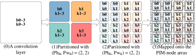
A DNN layer needs to be partitioned so that it can be processed in parallel on the allocated PIM-node array[13, 16]. Mapping a layer onto a PIM-node array means the layer should be partitioned into part-layers. Different partition schemes result in different-shaped part-layers and different data requirements of the PIM-nodes, which influence the computing efficiency in each PIM-node and the amount of inter-PIM-node communication.
To represent how the loops of a DNN layer are partitioned, we use five bi-tuples (, , , , ) to denote the number of partitions for loop , , , and , respectively. An example of layer partitioning is shown in Figure 5. For each loop of the layer, the loop length is divided by to get the corresponding loop length of the part-layer. Loop and are not partitioned since they are relatively small.
The spatial mapping of the part-layers determines the communication distance for transferring data of each PIM-node and thus influences the inter-PIM-node communication overhead. The order of spatial mapping of the part-layers, , can be represented by a sequence of the loops , , , and . An example of the spatial order is shown in Figure 5.
For simplicity, we use LM(Layer Mapping Scheme) to denote the mapping scheme of a layer, which includes partition numbers (, , , , ) and .
III-D DRAM capacity allocation
The distributed data storing of DRAM-PIM systems makes the DRAM capacity of one PIM-node a constraint. Since NicePIM focuses on the inference process of DNNs, intermediate data can be discarded after being consumed while all the weights of the DNN should be stored in the DRAM-PIM system. The limited capacity of the DRAM may not be sufficient for one PIM-node to hold a whole replication of all weights of the DNN.
If the DRAM capacity allocated for one layer is not enough for each PIM-node to store a full replication of the weights, we make each PIM-node only store one part of the weights and PIM-nodes share the weights through NoC before processing the layer. The weight-sharing process introduces extra inter-PIM-node communication cost. The less weight stored in PIM-nodes, the more required communication, which means we need to specify the number of weight replication for each layer. We use the number WR(Weight Replication number) to represent the allowed number of replications of weights of one layer. Denoting the number of PIM-nodes that require the same weights as , if is smaller than , each PIM-node stores part of the weights and the remainder parts are got from other PIM-nodes. Denoting the DRAM capacity of a PIM-node as , for each PIM-node, the summation of the stored weights of all layers in that PIM-node should be smaller than .
III-E Data layout pattern in DRAM
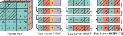
The pattern that the high-dimensional data of DNNs are flattened and stored in DRAM affects the efficiency of DRAM access. DRAM reaches its best performance and efficiency at sequential access since data access are performed via the row buffer. Row buffer miss or conflict will introduce extra energy and latency [36] and the energy and latency cost of DRAM can be summarized as the summation of the cost of data access and row buffer updating. Besides, with DNN quantization widely used, the data width in DNNs is often much smaller than the width of DRAM banks(8/16-bit per data v.s. 128bit per DRAM bank). If a PIM-node has more than one DRAM bank, the width difference between data and DRAM banks is even more critical. Since weights are read-only and can be re-arranged according to the access pattern in advance before being stored into the DRAM banks, we only focus on the data layout of input data and output data of DNN layers.
To make DRAM access requirements more sequential, two data layout orders, BCHW and BHWC, are taken into account, which is illustrated in Figure 6. To make full use of the width of DRAM banks, data grouping is employed before storing them into DRAM. An example of data grouping is shown in Figure 6 where the indicates 2 channels of feature maps are grouped. If a window of the first two channels is selected to do convolution, the data layout with BCHW[C2] requires 6 times DRAM access while the data layout with BCHW and BHWC requires 9 and 8 times respectively. We use and (Data Layout Pattern) to represent the data grouping and layout order of the input and output data of a layer. The and of a layer can be different but for layers with data dependency, the of the predecessor layer should be the same as the of the successor layer since they stand for the same data. For simplicity, we use DL, which includes and , to represent the data grouping and layout order of a DNN layer.
IV Overview of NicePIM
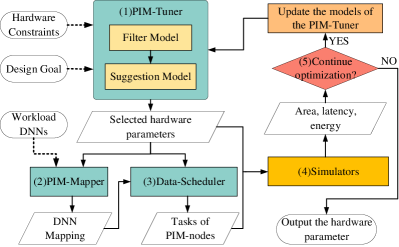
The overall flow of NicePIM is shown in Figure 7. The inputs of NicePIM include the hardware constraints, the design goal and the workload DNNs. The hardware constraints specify the attributes of the substrate of the hardware, such as the technology node, the total available area(), the shape of the array of DRAM banks(), the data width of each DRAM bank(), the capacity of one DRAM bank(), etc. The design goal quantifies the hardware quality with given hardware design parameters, which can be expressed by a cost function related to energy and latency of each workload DNN:
| (1) | |||
and are to adjust the preference on latency and energy and assigns different importance for each workload DNN.
The design space exploration process of NicePIM is iterative, which is shown in Figure 7: (1) The PIM-Tuner samples a large batch of hardware parameters from the whole design space. Then hardware parameters that are predicted to exceed the area constraint according to the filter model are discarded. The remaining hardware parameters are sorted by the suggestion model so that the ones with better predicted performance are selected. (2)For each set of hardware parameters given by PIM-Tuner, the DNN mapper generates corresponding DNN mapping schemes for all workload DNNs. (3)Each mapping scheme produced by PIM-Mapper is translated into tasks of PIM-nodes, during which the data-sharing process is scheduled by the Data-Scheduler. (4)The selected architectures from PIM-Tuner are sent to the simulator to get the area one-by-one until one architecture with legal area is obtained. Then that architecture and the corresponding tasks of PIM-nodes are passed to the simulators to get the latency and energy of each workload DNN. (5)If the ending condition is not met, the simulation results of area, latency and energy are added to the datasets of the PIM-Tuner for updating its two models and then the iteration is repeated.
V PIM-Tuner
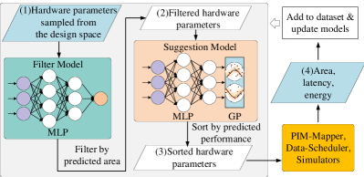
The design space of hardware parameters illustrated in Section III-A is so large(for example, about in Table II) that it is infeasible to find the optimal one by enumerating all points in the whole design space. For effectively characterizing the complicated design space of hardware parameters, in PIM-Tuner, we build a filter model to predict the area and a suggestion model to identify better architectures. The flow of PIM-Tuner is shown in Figure 8. The simulation results from previous iterations of the design space exploration flow are collected to form datasets for updating the models.
The suggestion model is a deep kernel learning model[27], which combines the robustness and non-parametric flexibility of Gaussian process with the expressive power of deep learning models. The input of the suggestion model is the normalized vector of hardware parameters and the model is fitted with the costs of the architectures with the corresponding hardware parameters, which are calculated by the function in Equation 1. In the updating process of the suggestion model, we learn the Gaussian process model and the DNN model jointly by maximizing the log marginal likelihood of the Gaussian process.
The DNN-based filter model is employed for identifying architectures that exceed the area constraint. Due to the 3D-stacking pattern of DRAM and logic, the area of the logic part of the DRAM-PIM accelerator is constrained by the DRAM part. Checking the area with simulators is time-consuming, so the filter model is necessary for reducing the times of invoking the simulators. The filter model gets hardware parameters as the input and outputs the corresponding area. We train the filter model using stochastic gradient descent algorithm with the mean squared error(MSE) between the output area and the simulated area as the loss function.
VI PIM-Mapper
For a DRAM-PIM accelerator with certain hardware parameters, the performance of DNNs on it depends on the DNN mapping scheme. As illustrated in Section III, different DNN layer partition schemes() result in different communication overhead and computing efficiency in each PIM-node. Proper parallelism between branches() can reduce the overhead of layer partitioning while maintaining a balanced load of PIM-nodes. The DRAM capacity allocation() influences the inter-PIM-node communication brought by weight-sharing among PIM-nodes. The data layout pattern in DRAM() affects the cost of DRAM access. The effect of each dimension in the mapping space is affected by the other dimensions, so only by considering all the dimensions in the design space of mapping can we get the optimal mapping scheme.
The PIM-Mapper considers all the aforementioned dimensions of mapping spaces and generates high-hardware-utilization DNN mappings on DRAM-PIM accelerators with given hardware parameters, the flow of which is shown in Algorithm 1. At the beginning of the optimization process, the PIM-Mapper firstly partitions the input DNN into segments as illustrated in Section III-B. Considering the constraint on between adjacent layers illustrated in Section III-E, we cannot only optimize the for one single layer but have to consider the detailed data dependency between layers of the DNN and choose for all layers. Thus, we employ an iterative alternated optimization process to optimize the mapping schemes, in which PIM-Mapper firstly optimizes all the , and with of all layers obtained in the previous iteration and then PIM-Mapper searches for the of all layers with the newly solved , and .
A dynamic programming algorithm is leveraged for optimizing , and . As illustrated in Section III-D, the value of of layers in the DNN is constrained by the DRAM capacity of the PIM-node. and together affect the latency of a layer and the effect of is influenced by the and of the corresponding layers. So we need to solve , and for the whole network simultaneously. To make full use of the DRAM capacity and explore a variety of with different parallelism between branches, we firstly generate several candidate , and for all segments and layers(line7~16 in Algorithm 1, illustrated in Section VI-A). Then we select the best combination of the candidates using a dynamic programming algorithm(line17~20 in Algorithm 1, illustrated in Section VI-B). Section VI-C explains the optimization process of of all the layers.
VI-A Mapping scheme candidate generation
In this step, for each segment, we generate candidate s with different parallelism between branches, and for each candidate, we generate candidate --pairs with different DRAM capacity requirements for making full use of the DRAM capacity of the PIM-node.
For each segment, we set different values of to get candidate s with different parallelism between its branches. For each value, the of each branch is determined by the number of operations with the objective of balancing the workloads of the . We leverage the slicing tree representation [37] to determine the positions and shapes of the , which means we iteratively partition the PIM-node array by two until all the are determined. The partitioning process follows the principle of maintaining the size of each proportional to the amount of operation of the layers to map so that the PIM-nodes in all can get a balanced load. The generated different mapping schemes of the -th segment, denoted as , are the candidates from which the final of that segment is chosen.
For each candidate of a segment, we set several values for each layer, ranging from the maximum value to 1, to set different DRAM capacity requirements for the layer. For each , we get the corresponding layer mapping scheme by traversing all possible choices and choosing the one with the lowest latency. The different values and the corresponding s form --pairs, and they are the candidates with different latency values and DRAM capacity requirements from which the final and of the layer are chosen. In the first iteration of PIM-Mapper when of all layers is not selected yet, we use the amount of DRAM access to estimate the latency of DRAM access and in the remainder iterations, both the amount of access and the data layout pattern are considered.
VI-B Dynamic-programming-based mapping scheme selection
The problem of selecting from the candidate s of all segments and --pairs of all layers is similar to the multiple-choice knapsack problem[38], which is to choose exactly one item from each class such that the profit sum is maximized without exceeding the capacity of the knapsack. We use a dynamic programming algorithm to solve the mapping scheme selection problem and the flow of the algorithm is shown in Algorithm 2. The inputs of the algorithm are the capacity() of DRAM of one PIM-node, different candidate s denoted as , different candidate --pairs of each layer under each and the corresponding latency() and required DRAM capacity() of each layer of each candidate. The output of the algorithm is the choice indexes of the candidates.
We use two tables, and , to store the latency with all DRAM capacity values. stores the latency of the first segments under the DRAM capacity requirement . Updated together with , two tables, and , are used to store the index of chosen for each segment and the index of chosen --pair for each layer, respectively. Another table, stores the latency result of the first layers in the -th Region of a segment under the DRAM capacity requirement . The choice index of --pair of each layer in that segment is stored in correspondingly.
Table is used to collect the latency of layers in one segment. For a segment with a certain , we add the latency results of all candidate --pairs of all layers in the segment into the and record the choice index in the , which is illustrated in line9~17 in Algorithm 2. During the process, each --pair candidate of each layer in the region is selected to calculate the new latency. If the new latency is better than the existing value in the table, that candidate is chosen and the and are updated.
Table is used to collect the latency of all segments. After the latency of a segment with all DRAM capacity values is obtained in the , we add the into , which is illustrated in line18~24 in Algorithm 2. The latency result that best improves the total latency under each DRAM capacity value is chosen to update the , and the and are updated correspondingly.
After all candidates of all segments are visited, the best choices can be acquired in and .
VI-C Optimization for data layout pattern
With chosen for each segment and --pairs for all layers, we then update the data layout pattern, , for each layer. Firstly, for each layer with the updated and , we enumerate all possible choices of and select the one with the lowest latency without considering the of other layers. Then we check the of each layer pair with data dependency and make the of the successor layer the same as the of the predecessor layer. If the of a layer is changed, we re-select its .
VII Data-Scheduler
In convolution layers and matrix-multiplication layers, there is a large amount of data reuse, and with layer partition methods illustrated in Section III-C, the temporal reuse of data is converted to spatial data-sharing between PIM-nodes. For example, if a layer is partitioned on , the PIM-nodes need to share inputs; if a layer is partitioned on , the PIM-nodes need to share weights. To reduce the latency of data-sharing by balancing the load of NoC links, we use a Hamilton-cycle-based data transfer strategy and build an ILP model to determine the Hamilton cycles. The data-sharing problem is defined in 1. Note that a layer can be partitioned on more than one dimension, so there may be multiple sharing-sets during one data-sharing process.
Definition 1
For a piece of data that is stored distributively in a set of PIM-nodes, each PIM-node gets the remaining data from the other PIM-nodes in the set so that eventually the PIM-node has the whole piece of data. The PIM-node set to share data is denoted as a sharing-set and the process for the PIM-nodes to get the data is the data-sharing process.
To achieve a balanced load of PIM-nodes, we use a Hamilton-cycle-based data transfer strategy to schedule the data-sharing process: for the PIM-nodes in a sharing-set with a Hamilton cycle connecting them, each PIM-node transfers the newly received data to the next PIM-node in the Hamilton cycle and the process is repeated until all PIM-nodes receive all the data. This strategy makes all PIM-nodes in the sharing-set have equal-sized data to send and receive from NoC.
In each step of the Hamilton-cycle-based data-sharing process, the load of the NoC links is determined by the specific Hamilton cycle thus different Hamilton cycle leads to different data transfer latency. We build an ILP model to determine the Hamilton cycles simultaneously for all sharing-sets in one data-sharing process. For sharing-sets where each set has PIM-nodes, we denote the coordinate of each PIM-node as . We use a binary decision variable to denote the selected connection from to in the -th sharing-set. The following constraints ensure the selected connections form Hamilton cycles, where integer auxiliary variables are introduced for eliminating subtours[39].
| (2) |
| (3) | |||
The latency of data transfer is determined by the link with the heaviest load, so the objective function is to minimize the maximum load of all links in the NoC, which is as follows:
| (4) |
is 1 if the routing path from PIM-node with index to the PIM-node with index passes , and otherwise its value is .
VIII Experiments
We implement NicePIM on a Linux server with four 18-core Intel Xeon CPUs and four nVidia Tesla V100 GPUs. We use Pytorch[40] and Botorch[41] to build and train the models of the PIM-Tuner. The PIM-Mapper is implemented using Python language. We use Gurobi[42] to solve the ILP model in the Data-Scheduler.
VIII-A Evaluation methods
We leverage the DNN accelerator evaluation tool, Timeloop+Accelergy[22, 23], to get the area of the NN engine of the DRAM-PIM architecture. The intra- and inter-PIM-node DRAM access is simulated by the Ramulator-PIM[43, 44] integrated with BookSim2.0[45], which are both cycle-accurate simulation tools. The DRAMPower[46] integrated into Ramulator-PIM helps to get the energy cost of DRAM. The latency and energy cost of PE array and buffers for computation tasks are simulated by Timeloop+Accelergy.
VIII-B Experiment setup
The input hardware constraints of NicePIM are shown in Table II. The stacked 3D-DRAM has 256 banks with technology node and each bank has capacity. The energy cost of DRAM access is according to the test result in [10]. The DRAM banks are organized into a array so that the PIM-node array has a maximum height and width of both 16. The total available area of the logic die for the NN engines is , which is inferred from a fabricated PIM chip[15]. PIM-nodes run with a clock frequency of 400 MHz and the technology node of logic die is . Each PIM-node can have an up to PE array and up to buffers for inputs, weights and outputs. The data width of input data and output data of DNN layers is set to 16-bit and the intermediate partial-sums are 32-bit. The width of NoC flits is set to half the total width of DRAM banks of a PIM-node and the energy cost is estimated as [47]. The routers are organized into mesh topology and the dimension-order routing strategy is leveraged with 8 virtual channels.
The MLP of the filter model of the PIM-Mapper has four layers with 256, 64, 16 and 1 output neurons and the MLP of the suggestion model has three layers with 256, 64 and 16 output neurons. The activation functions of both models are ReLU. Adam optimizer[48] is leveraged to train the models. In each iteration, PIM-Tuner randomly samples architectures from the design space until gets 16384 legal architectures by the filter model. The of the PIM-Mapper is set to 3.
Several DNNs from different fields are used as workloads for evaluation, including GoogLeNet[21], ResNet[29], VGG[30], DarkNet53[31] and BERT[20]. GoogLeNet, VGG16 and ResNet152 are CNNs for classifying images. VGG16 has a straight-line structure while ResNet152 and GoogLeNet have multi-branch structures with short-cut connections and inception-blocks, respectively. DarkNet53 is the backbone of the YOLOv3 network used for object detection which has short-cut structures similar to ResNet152. BERT is a kind of Transformer network for natural language processing and we use the BERT-Base model which has 12 heads in one Transformer block.
| Type | Hardware Parameter | Value |
|---|---|---|
| Constant | Technology node | |
| Variable | ||
VIII-C Results of NicePIM
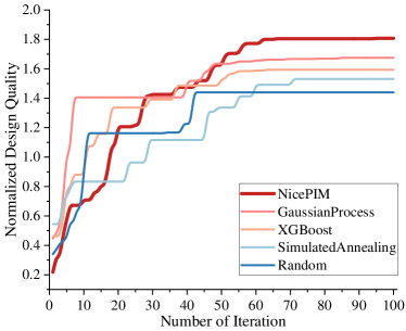
Figure 9 shows the achieved design quality of NicePIM along with iteration process. The optimization goal in Equation 1 is set to and , which indicates the energy-delay-product(EDP). We use the reciprocal of the summed cost of the five DNNs as the metric of the design quality.
Some other design space exploration methods are evaluated as comparisons, the results of which are shown in Figure 9. PIM-Mapper and Data-Scheduler are also used with these algorithms for fair comparison. In the Random method, the architecture to evaluate is randomly chosen in each iteration. Another widely used random search algorithm, simulated annealing, is also evaluated. Besides, we replace the suggestion model of the PIM-Tuner with other machine learning models. In the GaussianProcess and XGBoost method, the suggestion model is replaced by Gaussian process and XGBoost[49], respectively. The result in Figure 9 shows that the NicePIM achieves the most significant improvement in design quality. The random search algorithms cannot obtain enough information from the already explored architectures while the other two machine learning models are less accurate in characterizing the design space than the suggestion model in the PIM-Mapper.
Besides, we compare the performance of the nVidia Tesla V100 GPU with the DRAM-PIM architecture given by NicePIM, which has PIM-nodes and each PIM-node has a PE array with 16KiB, 144KiB and 32KiB buffers for inputs, weights and outputs, respectively. We try different batch sizes for both systems and choose the best averaged latency per sample as the final performance. For DRAM-PIM accelerator, the batch size is changed from 1 to 16, and for GPU, we try batch size from 1 to 1024. For fair comparison, we scale the latency results with the area, frequency and technology node. The simulated latency of the DRAM-PIM architecture given by NicePIM is 25x smaller than the tested latency on GPU on average, which means NicePIM makes proper use of the area of the DRAM-PIM system.
VIII-D Effectiveness of the PIM-Mapper
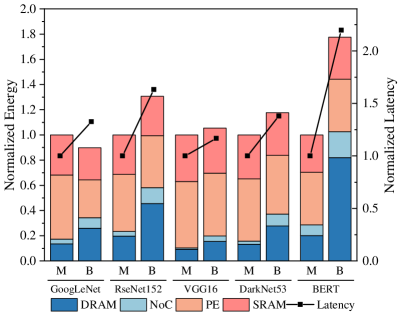
We evaluate the five DNNs with a batch size of to illustrate the effectiveness of the PIM-Mapper on two DRAM-PIM systems with and PIM-node arrays. In the PIM system, we set a PE array and for all SRAM buffers in a PIM-node. As for the PIM system, the settings are and .
The results are compared with a baseline method with sequential mapping scheme. In baseline method, each layer is mapped onto the whole PIM-node array and we use Timeloop[22] to solve the of the layers with the optimization goal set to “Delay”. The of each layer in the baseline method is initially set to the maximum value and if the DRAM capacity is not enough, we iteratively reduce the value from the layers with the largest number of weights until the DRAM capacity constraint is met. The of all layers is set to be the same. We try several such as , and , and select the one with the best latency result. The data-sharing process in the baseline method is also scheduled by our proposed Data-Scheduler.
The experimental results in Figure 10 show that the PIM-Mapper can generate high-utilization and low-energy mappings for PIM systems with different hardware configurations. The latency is reduced by 37% on average and the energy cost is reduced by 28% on average. On the PIM system, where each PIM-node has 16 DRAM banks, the energy cost on DRAM of PIM-Mapper is significantly better than that of the baseline, which means PIM-Mapper better optimizes the of layers and makes more sufficient use of the bandwidth of DRAM. On the PIM system where there are more but smaller PIM-nodes, the energy cost on NoC of PIM-Mapper is much lower than the baseline method, which indicates PIM-Mapper achieves lower inter-PIM-node communication overhead. One reason is that PIM-Mapper better utilizes the parallelism between DNN branches. Besides, the better DRAM capacity allocation strategy in PIM-Mapper also helps to reduce the overhead for sharing weights.
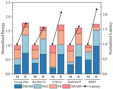
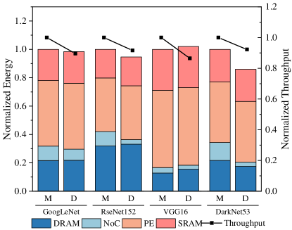
We also compare the PIM-Mapper with DDAM, a CNN mapping framework for DRAM-PIM systems[47]. DDAM partitions the CNN into several parts and maps them onto different regions of the DRAM-PIM system. A dynamic programming algorithm is employed to balance the load of the regions of the DRAM-PIM system for high throughput. Since DDAM makes CNNs processed in a pipeline manner, we compare the performance on throughput of the two frameworks by changing the batch size from 1 to 16 and choosing the best result. The experimental results in Figure 11 show that PIM-Mapper achieves better throughput with an average improvement of 11%. Mapping configurations such as data layout pattern and inter-branch parallelism are not taken into account in DDAM which affects its throughput. Moreover, DDAM cannot achieve perfect load balance for regions so the utilization of the PIM-node array decreases. DDAM and PIM-Mapper have similar energy cost except that of NoC, which is much smaller in the result of DDAM. The pipeline-mapping manner leveraged by DDAM can make each layer mapped onto a small region of the DRAM-PIM system and thus the inter-PIM-node communication can be reduced a lot. But it is worth noting that the pipeline-mapping scheme employed in DDAM can only be used to optimize the throughput and the latency is 10x worse than PIM-Mapper.
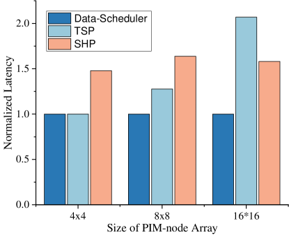
VIII-E Effectiveness of the Data-Scheduler
Figure 12 shows the comparison of the proposed Data-Scheduler against the other two scheduling methods(TSP and SHP). The method named TSP proposed in [47] also uses a Hamilton-cycle-based data-transfer pattern while the Hamilton cycle is built by formulating a traveling-sales-man problem. The SHP method finds the shortest path for each part of the data and then the part-data is transferred along the path, which ensures the smallest hops to transfer all the data. We set three sizes for the PIM-node array for evaluation, which are , and and the sizes of sharing set are all 16. On the and PIM-node array, there are multiple sharing sets and they are placed in an interleaving manner: the distances on height and width of adjacent PIM-nodes in the same sharing set are all 2 and 4, respectively. For all the PIM-node array sizes, each PIM-node has 8 KiB data to share and the flit width of NoC is 64-bit.
The results in Figure 12 illustrate that the proposed ILP-based scheduling method achieves the smallest latency since the load of links is taken into account. The SHP method only reduces the hops to transfer data but cannot balance the load of both PIM-nodes and links. The TSP method also uses the Hamilton path to schedule the data transfer process so that the load of PIM-nodes is balanced. However, the load of links is not taken into account in the TSP method, so the latency is still large in some cases.
IX Related Work
IX-A PIM accelerators with tiled architecture
Tiled architecture is employed by many 3D-stacking-based PIM accelerators since it has good scalability and matches well with 3D-stacking pattern. Kim et al. designed a programmable neuromorphic architecture based on Micron’s HMC[9] named Neurocube[13] as well as a simple mapping strategy that partitions the feature maps of CNNs. Gao et al. designed TETRIS[16], an HMC-based NN accelerator with data-bypass and in-memory accumulation. TETRIS employs a greedy layer-by-layer partitioning strategy to map CNNs. Wang et al.[18] proposed a memory-efficient data allocation strategy for CNNs on 3D-stacked PIM architecture. QUEST[33] is a 3D-stacked-SRAM-based DNN accelerator and supports log-quantized DNN processing. These works mainly focus on the architecture design and scheduling of one PIM-node and use simple DNN mapping strategies. DDAM [47] is a CNN mapping framework that partitions the CNN into many parts and maps each part onto the different region of the DRAM-PIM system, making the parts processed in a pipeline manner. DDAM can achieve high throughput of CNNs but cannot be used to optimize the latency. The hardware design parameters in these aforementioned works and their mapping strategies may not be suitable when the hardware configuration or the target workloads changes.
IX-B Design space exploration for DNN accelerators
The widespread use of DNNs introduces various performance and energy requirements of the accelerators and DNN accelerators have many design parameters to choose. Many works are proposed to efficiently explore the design space and find proper design parameters for their target DNN accelerator architectures. Timeloop+Accelergy [22, 23] uses a constraint-driven random search method with a fine-grained model for analyzing DNN accelerators to generate valid mappings for DNN layers. MAGNet[24] has a highly configurable architecture template for DNN accelerators and used Bayesian optimization and random sampling to optimize the hardware configuration, DNN mapping and DNN model. ZigZag[25] employs the Memory-Centric Design Space Representation for DNN accelerators and provides heuristic and iterative search strategies to rapidly locate optimal mapping. ZigZag is also able to generate the optimal architecture by exhaustive search. FAST[26] is a framework that jointly explores the hardware datapath configuration, software schedule, and compiler operations for DNN accelerators with detailed DNN performance characterization and a novel op fusion technique. To search for effective DNN mapping and efficient hardware configuration, these works have diverse prior definitions on the architecture and DNN mapping, which make them not suitable when facing the design space of DRAM-PIM architectures.
X Conclusion
This paper proposes a framework that optimizes the DNN mapping and hardware parameters for DRAM-PIM-based DNN accelerators. The PIM-Mapper together with the Data-Scheduler can effectively reduce the inference latency and the energy cost of DNNs on DRAM-PIM architectures with various hardware parameters. The PIM-Tuner is effective to extract features from the hardware design space so that the obtained architecture has higher quality compared to other design space exploration methods.
References
- [1] Y. Chen, T. Luo et al., “DaDianNao: A Machine-Learning Supercomputer,” in 2014 47th Annual IEEE/ACM International Symposium on Microarchitecture. Cambridge, United Kingdom: IEEE, Dec. 2014, pp. 609–622. [Online]. Available: http://ieeexplore.ieee.org/document/7011421/
- [2] Z. Du, R. Fasthuber et al., “ShiDianNao: shifting vision processing closer to the sensor,” in Proceedings of the 42nd Annual International Symposium on Computer Architecture, ser. ISCA ’15. New York, NY, USA: Association for Computing Machinery, Jun. 2015, pp. 92–104. [Online]. Available: https://doi.org/10.1145/2749469.2750389
- [3] M. Alwani, H. Chen et al., “Fused-layer CNN accelerators,” in 2016 49th Annual IEEE/ACM International Symposium on Microarchitecture (MICRO). Taipei, Taiwan: IEEE, Oct. 2016, pp. 1–12. [Online]. Available: http://ieeexplore.ieee.org/document/7783725/
- [4] Y.-H. Chen, J. Emer, and V. Sze, “Eyeriss: A Spatial Architecture for Energy-Efficient Dataflow for Convolutional Neural Networks,” in 2016 ACM/IEEE 43rd Annual International Symposium on Computer Architecture (ISCA). Seoul, South Korea: IEEE, Jun. 2016, pp. 367–379. [Online]. Available: http://ieeexplore.ieee.org/document/7551407/
- [5] N. P. Jouppi, C. Young et al., “In-Datacenter Performance Analysis of a Tensor Processing Unit,” in Proceedings of the 44th Annual International Symposium on Computer Architecture. Toronto ON Canada: ACM, Jun. 2017, pp. 1–12. [Online]. Available: https://dl.acm.org/doi/10.1145/3079856.3080246
- [6] J. Li, G. Yan et al., “SmartShuttle: Optimizing off-chip memory accesses for deep learning accelerators,” in 2018 Design, Automation & Test in Europe Conference & Exhibition (DATE). Dresden, Germany: IEEE, Mar. 2018, pp. 343–348. [Online]. Available: http://ieeexplore.ieee.org/document/8342033/
- [7] X. Wei, Y. Liang, and J. Cong, “Overcoming Data Transfer Bottlenecks in FPGA-based DNN Accelerators via Layer Conscious Memory Management,” in Proceedings of the 56th Annual Design Automation Conference 2019. Las Vegas NV USA: ACM, Jun. 2019, pp. 1–6. [Online]. Available: https://dl.acm.org/doi/10.1145/3316781.3317875
- [8] X. Chen, Y. Han, and Y. Wang, “Communication Lower Bound in Convolution Accelerators,” in 2020 IEEE International Symposium on High Performance Computer Architecture (HPCA), 2020, pp. 529–541, iSSN: 2378-203X.
- [9] “Hybrid Memory Cube – HMC Gen2,” p. 105, 2018. [Online]. Available: https://www.micron.com/-/media/client/global/documents/products/data-sheet/hmc/gen2/hmc_gen2.pdf
- [10] B. Fujun, J. Xiping et al., “A Stacked Embedded DRAM Array for LPDDR4/4X using Hybrid Bonding 3D Integration with 34GB/s/1Gb 0.88pJ/b Logic-to-Memory Interface,” in 2020 IEEE International Electron Devices Meeting (IEDM). San Francisco, CA, USA: IEEE, Dec. 2020, pp. 6.6.1–6.6.4. [Online]. Available: https://ieeexplore.ieee.org/document/9372039/
- [11] K. Shiba, T. Omori et al., “A 96-MB 3D-Stacked SRAM Using Inductive Coupling With 0.4-V Transmitter, Termination Scheme and 12:1 SerDes in 40-nm CMOS,” IEEE Transactions on Circuits and Systems I: Regular Papers, vol. 68, no. 2, pp. 692–703, Feb. 2021. [Online]. Available: https://ieeexplore.ieee.org/document/9272691/
- [12] M. Horowitz, “1.1 Computing’s energy problem (and what we can do about it),” in 2014 IEEE International Solid-State Circuits Conference Digest of Technical Papers (ISSCC), 2014, pp. 10–14, iSSN: 2376-8606.
- [13] D. Kim, J. Kung et al., “Neurocube: A Programmable Digital Neuromorphic Architecture with High-Density 3D Memory,” in 2016 ACM/IEEE 43rd Annual International Symposium on Computer Architecture (ISCA). Seoul, South Korea: IEEE, Jun. 2016, pp. 380–392. [Online]. Available: http://ieeexplore.ieee.org/document/7551408/
- [14] X. Jiang, F. Zuo et al., “A 1596GB/s 48Gb Embedded DRAM 384-Core SoC with Hybrid Bonding Integration,” in 2021 IEEE Asian Solid-State Circuits Conference (A-SSCC), 2021, pp. 1–3.
- [15] D. Niu, S. Li et al., “184QPS/W 64Mb/mm23D Logic-to-DRAM Hybrid Bonding with Process-Near-Memory Engine for Recommendation System,” in 2022 IEEE International Solid- State Circuits Conference (ISSCC), vol. 65, 2022, pp. 1–3, iSSN: 2376-8606.
- [16] M. Gao, J. Pu et al., “TETRIS: Scalable and Efficient Neural Network Acceleration with 3D Memory,” in Proceedings of the Twenty-Second International Conference on Architectural Support for Programming Languages and Operating Systems. Xi’an China: ACM, Apr. 2017, pp. 751–764. [Online]. Available: https://dl.acm.org/doi/10.1145/3037697.3037702
- [17] Y. Wang, M. Zhang, and J. Yang, “Exploiting Parallelism for Convolutional Connections in Processing-In-Memory Architecture,” in Proceedings of the 54th Annual Design Automation Conference 2017. Austin TX USA: ACM, Jun. 2017, pp. 1–6. [Online]. Available: https://dl.acm.org/doi/10.1145/3061639.3062242
- [18] Y. Wang, W. Chen et al., “Towards Memory-Efficient Allocation of CNNs on Processing-in-Memory Architecture,” IEEE Transactions on Parallel and Distributed Systems, vol. 29, no. 6, pp. 1428–1441, Jun. 2018. [Online]. Available: https://ieeexplore.ieee.org/document/8252752/
- [19] C. Min, J. Mao et al., “NeuralHMC: an efficient HMC-based accelerator for deep neural networks,” in Proceedings of the 24th Asia and South Pacific Design Automation Conference. Tokyo Japan: ACM, Jan. 2019, pp. 394–399. [Online]. Available: https://dl.acm.org/doi/10.1145/3287624.3287642
- [20] J. Devlin, M.-W. Chang et al., “BERT: Pre-training of Deep Bidirectional Transformers for Language Understanding,” May 2019, arXiv:1810.04805 [cs]. [Online]. Available: http://arxiv.org/abs/1810.04805
- [21] C. Szegedy, Wei Liu et al., “Going deeper with convolutions,” in 2015 IEEE Conference on Computer Vision and Pattern Recognition (CVPR). Boston, MA, USA: IEEE, Jun. 2015, pp. 1–9. [Online]. Available: http://ieeexplore.ieee.org/document/7298594/
- [22] A. Parashar, P. Raina et al., “Timeloop: A Systematic Approach to DNN Accelerator Evaluation,” in 2019 IEEE International Symposium on Performance Analysis of Systems and Software (ISPASS). Madison, WI, USA: IEEE, Mar. 2019, pp. 304–315. [Online]. Available: https://ieeexplore.ieee.org/document/8695666/
- [23] Y. N. Wu, J. S. Emer, and V. Sze, “Accelergy: An Architecture-Level Energy Estimation Methodology for Accelerator Designs,” in 2019 IEEE/ACM International Conference on Computer-Aided Design (ICCAD). Westminster, CO, USA: IEEE, Nov. 2019, pp. 1–8. [Online]. Available: https://ieeexplore.ieee.org/document/8942149/
- [24] R. Venkatesan, P. Raina et al., “MAGNet: A Modular Accelerator Generator for Neural Networks,” in 2019 IEEE/ACM International Conference on Computer-Aided Design (ICCAD). Westminster, CO, USA: IEEE, Nov. 2019, pp. 1–8. [Online]. Available: https://ieeexplore.ieee.org/document/8942127/
- [25] L. Mei, P. Houshmand et al., “ZigZag: Enlarging Joint Architecture-Mapping Design Space Exploration for DNN Accelerators,” IEEE Transactions on Computers, vol. 70, no. 8, pp. 1160–1174, 2021, conference Name: IEEE Transactions on Computers.
- [26] D. Zhang, S. Huda et al., “A full-stack search technique for domain optimized deep learning accelerators,” in Proceedings of the 27th ACM International Conference on Architectural Support for Programming Languages and Operating Systems. Lausanne Switzerland: ACM, Feb. 2022, pp. 27–42. [Online]. Available: https://dl.acm.org/doi/10.1145/3503222.3507767
- [27] A. G. Wilson, Z. Hu et al., “Deep Kernel Learning,” Nov. 2015, arXiv:1511.02222 [cs, stat]. [Online]. Available: http://arxiv.org/abs/1511.02222
- [28] A. Krizhevsky, I. Sutskever, and G. E. Hinton, “ImageNet classification with deep convolutional neural networks,” Communications of the ACM, vol. 60, no. 6, pp. 84–90, May 2017. [Online]. Available: https://dl.acm.org/doi/10.1145/3065386
- [29] K. He, X. Zhang et al., “Deep Residual Learning for Image Recognition,” in 2016 IEEE Conference on Computer Vision and Pattern Recognition (CVPR), Jun. 2016, pp. 770–778, iSSN: 1063-6919.
- [30] K. Simonyan and A. Zisserman, “Very Deep Convolutional Networks for Large-Scale Image Recognition,” arXiv:1409.1556 [cs], Apr. 2015, arXiv: 1409.1556. [Online]. Available: http://arxiv.org/abs/1409.1556
- [31] J. Redmon and A. Farhadi, “YOLOv3: An Incremental Improvement,” arXiv:1804.02767 [cs], Apr. 2018, arXiv: 1804.02767 version: 1. [Online]. Available: http://arxiv.org/abs/1804.02767
- [32] I. Bello, W. Fedus et al., “Revisiting ResNets: Improved Training and Scaling Strategies,” arXiv:2103.07579 [cs], Mar. 2021, arXiv: 2103.07579. [Online]. Available: http://arxiv.org/abs/2103.07579
- [33] K. Ueyoshi, K. Ando et al., “QUEST: Multi-Purpose Log-Quantized DNN Inference Engine Stacked on 96-MB 3-D SRAM Using Inductive Coupling Technology in 40-nm CMOS,” IEEE Journal of Solid-State Circuits, vol. 54, no. 1, pp. 186–196, Jan. 2019. [Online]. Available: https://ieeexplore.ieee.org/document/8492341/
- [34] F. Sijstermans, “The nvidia deep learning accelerator,” in Hot Chips, Mar. 2018.
- [35] Y. S. Shao, J. Clemons et al., “Simba: Scaling Deep-Learning Inference with Multi-Chip-Module-Based Architecture,” in Proceedings of the 52nd Annual IEEE/ACM International Symposium on Microarchitecture. Columbus OH USA: ACM, Oct. 2019, pp. 14–27. [Online]. Available: https://dl.acm.org/doi/10.1145/3352460.3358302
- [36] R. V. W. Putra, M. A. Hanif, and M. Shafique, “ROMANet: Fine-Grained Reuse-Driven Off-Chip Memory Access Management and Data Organization for Deep Neural Network Accelerators,” IEEE Transactions on Very Large Scale Integration (VLSI) Systems, vol. 29, no. 4, pp. 702–715, Apr. 2021. [Online]. Available: https://ieeexplore.ieee.org/document/9369858/
- [37] M. Lai and D. Wong, “Slicing tree is a complete floorplan representation,” in Proceedings Design, Automation and Test in Europe. Conference and Exhibition 2001, Mar. 2001, pp. 228–232, iSSN: 1530-1591.
- [38] H. Kellerer, U. Pferschy, and D. Pisinger, “The Multiple-Choice Knapsack Problem,” in Knapsack Problems. Springer, Berlin, Heidelberg, 2004, pp. 317–347. [Online]. Available: https://link.springer.com/chapter/10.1007/978-3-540-24777-7_11
- [39] C. E. Miller, A. W. Tucker, and R. A. Zemlin, “Integer Programming Formulation of Traveling Salesman Problems,” Journal of the ACM, vol. 7, no. 4, pp. 326–329, Oct. 1960. [Online]. Available: https://dl.acm.org/doi/10.1145/321043.321046
- [40] A. Paszke, S. Gross et al., “PyTorch: An Imperative Style, High-Performance Deep Learning Library,” Dec. 2019, arXiv:1912.01703 [cs, stat]. [Online]. Available: http://arxiv.org/abs/1912.01703
- [41] M. Balandat, B. Karrer et al., “BoTorch: A Framework for Efficient Monte-Carlo Bayesian Optimization,” Dec. 2020, arXiv:1910.06403 [cs, math, stat]. [Online]. Available: http://arxiv.org/abs/1910.06403
- [42] Gurobi Optimization, LLC, “Gurobi Optimizer Reference Manual,” 2022. [Online]. Available: https://www.gurobi.com
- [43] Y. Kim, W. Yang, and O. Mutlu, “Ramulator: A Fast and Extensible DRAM Simulator,” IEEE Computer Architecture Letters, vol. 15, no. 1, pp. 45–49, Jan. 2016. [Online]. Available: http://ieeexplore.ieee.org/document/7063219/
- [44] G. Singh, J. Gómez-Luna et al., “NAPEL: Near-Memory Computing Application Performance Prediction via Ensemble Learning,” in Proceedings of the 56th Annual Design Automation Conference 2019. Las Vegas NV USA: ACM, Jun. 2019, pp. 1–6. [Online]. Available: https://dl.acm.org/doi/10.1145/3316781.3317867
- [45] N. Jiang, D. U. Becker et al., “A detailed and flexible cycle-accurate Network-on-Chip simulator,” in 2013 IEEE International Symposium on Performance Analysis of Systems and Software (ISPASS), Apr. 2013, pp. 86–96.
- [46] C. Karthik, W. Christian et al., “DRAMPower: Open-source DRAM Power & Energy Estimation Tool,” 2022. [Online]. Available: http://www.drampower.info
- [47] J. Wang, H. Du et al., “DDAM: Data Distribution-Aware Mapping of CNNs on Processing-In-Memory Systems,” ACM Transactions on Design Automation of Electronic Systems, vol. 28, no. 3, pp. 1–30, May 2023. [Online]. Available: https://dl.acm.org/doi/10.1145/3576196
- [48] D. P. Kingma and J. Ba, “Adam: A Method for Stochastic Optimization,” Jan. 2017, arXiv:1412.6980 [cs]. [Online]. Available: http://arxiv.org/abs/1412.6980
- [49] T. Chen and C. Guestrin, “XGBoost: A Scalable Tree Boosting System,” in Proceedings of the 22nd ACM SIGKDD International Conference on Knowledge Discovery and Data Mining. San Francisco California USA: ACM, Aug. 2016, pp. 785–794. [Online]. Available: https://dl.acm.org/doi/10.1145/2939672.2939785