Hardware-aware Training Techniques for Improving Robustness of Ex-Situ Neural Network Transfer onto Passive TiO ReRAM Crossbars
Abstract
Passive resistive random access memory (ReRAM) crossbar arrays, a promising emerging technology used for analog matrix-vector multiplications, are far superior to their active (1T1R) counterparts in terms of the integration density. However, current transfers of neural network weights into the conductance state of the memory devices in the crossbar architecture are accompanied by significant losses in precision due to hardware variabilities such as sneak path currents, biasing scheme effects and conductance tuning imprecision. In this work, training approaches that adapt techniques such as dropout, the reparametrization trick and regularization to TiO crossbar variabilities are proposed in order to generate models that are better adapted to their hardware transfers. The viability of this approach is demonstrated by comparing the outputs and precision of the proposed hardware-aware network with those of a regular fully connected network over a few thousand weight transfers using the half moons dataset in a simulation based on experimental data. For the neural network trained using the proposed hardware-aware method, 79.5% of the test set’s data points can be classified with an accuracy of 95% or higher, while only 18.5% of the test set’s data points can be classified with this accuracy by the regularly trained neural network.
I Introduction
As neural networks’ complex problem-solving capabilities increase, so do their energetic and computational demands. These demands have grown so much that the use of graphics processing units (GPUs) and data centers is proving to be essential for practical machine learning. Meanwhile, a plethora of applications at the edge would greatly benefit from the use of neural networks but cannot always use these deep networks due to their high energy demands edge-computing-review . As the main limitations of neural network computations stem from the von Neumann bottleneck between the memory and processor Li2015 , in-memory computing with analog, non-volatile emerging resistive memories is among the most promising avenues of innovation that can be used to overcome this problem Amirsoleimani2020 ; Jeong2016 ; Ielmini2020 . Non-volatile memories exploit metal oxide mesoudy2021CMOS ; Dalgaty2021 ; Kim2021 ; Bayat2018 , phase-change phase-change or ferroelectric materials Nishitani2012 , among other things, to perform computations directly in memory, decreasing the need to fetch data to perform computations. In a crossbar configuration, in-memory computing relies on the fundamental Ohm’s and Kirchoff’s laws, which enable an energy-efficient version of the vector matrix multiplications (VMMs) at the core of neural networks. These memory devices are versatile and have proven their potential for many different types of neural networks, such as long short-term memory (LSTMs) LSTM-hardware-aware ; LSTM-ReRAM , generative adversarial networks (GAN) Chen2022 and Bayesian NNs BNNrealizationReRAM ; zhou_bayesian_2021 ; BNNexploitingReRAM . Neural networks on crossbars always require either in-situ or ex-situ learning techniques. Both of which have been demonstrated on crossbars Alibart2013 . The former technique trains the network online on the devices by implementing backpropagation through tuning pulses. The latter performs the training offline and thereafter the network is transferred to the crossbars by converting the obtained trained weights into conductances. The more commonly used ex-situ technique is much simpler but hardly considers hardware variabilities during training. This renders it less robust to all potential hardware non-idealities.
The crossbar architectures presented in the literature are often based on the 1T1R integration scheme Xue2020154A2 ; Yao2017 , where a transistor (1T) is cascaded with each memory (1R) to allow independent accesses to desired memories without disturbing adjacent devices. This improved control provides high programming and reading accuracies but leads to a lower integration density, higher wiring complexity and increased fabrication costs. On the other hand, passive (0T1R) crossbars exhibit excellent scalability and lower fabrication costs. In Xia2019 , a factor of 20 between the sizes of individual 1T1R (4 m) and 0T1R ( nm) memristors was reported. An average relative conductance import accuracy of 1% on a fully passive crossbar with a size of 6464 was reported Kim2021 . This crossbar had of memristors functioning. As such, passive crossbars hold much promise for the future of in-memory computing with ReRAM devices.
However, these passive crossbars present multiple inherent sources of variability varia_memristor , which currently hinder their use at large scale. The conductance tuning imprecision that is observed when a device is programmed to a certain conductive level, unsatisfactory device yields, asymmetrical switching dynamics, the conductance drift due to relaxation effects over time and sneak path currents are a few examples of the issues afflicting this technology. These non-idealities directly affect the results of analog matrix-vector multiplications (VMM). Cumulatively, they often lead to incorrect classifications. While some of these non-idealities can be harnessed to implement efficient stochastic neural network models in hardware Yon2022 ; Dalgaty2021 ; BNNexploitingReRAM ; LSTM-hardware-aware , they remain very detrimental for standard in-memory computing solutions and make it difficult to scale up this technology. A potential avenue that can be used to mitigate the sneak path current problems is the use of tiled crossbars; the neural network weights can be separated onto sub-crossbars called tiles. Tiles are compatible with control transistors and circuitry. These 88 crossbar tiles offer an intermediate solution that lies between the improved controllability of 1T1R crossbars and the scalability of 0T1R crossbars.
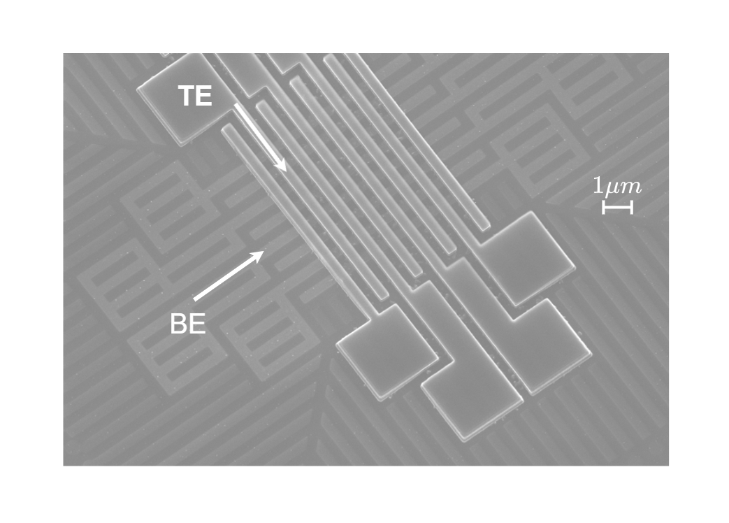
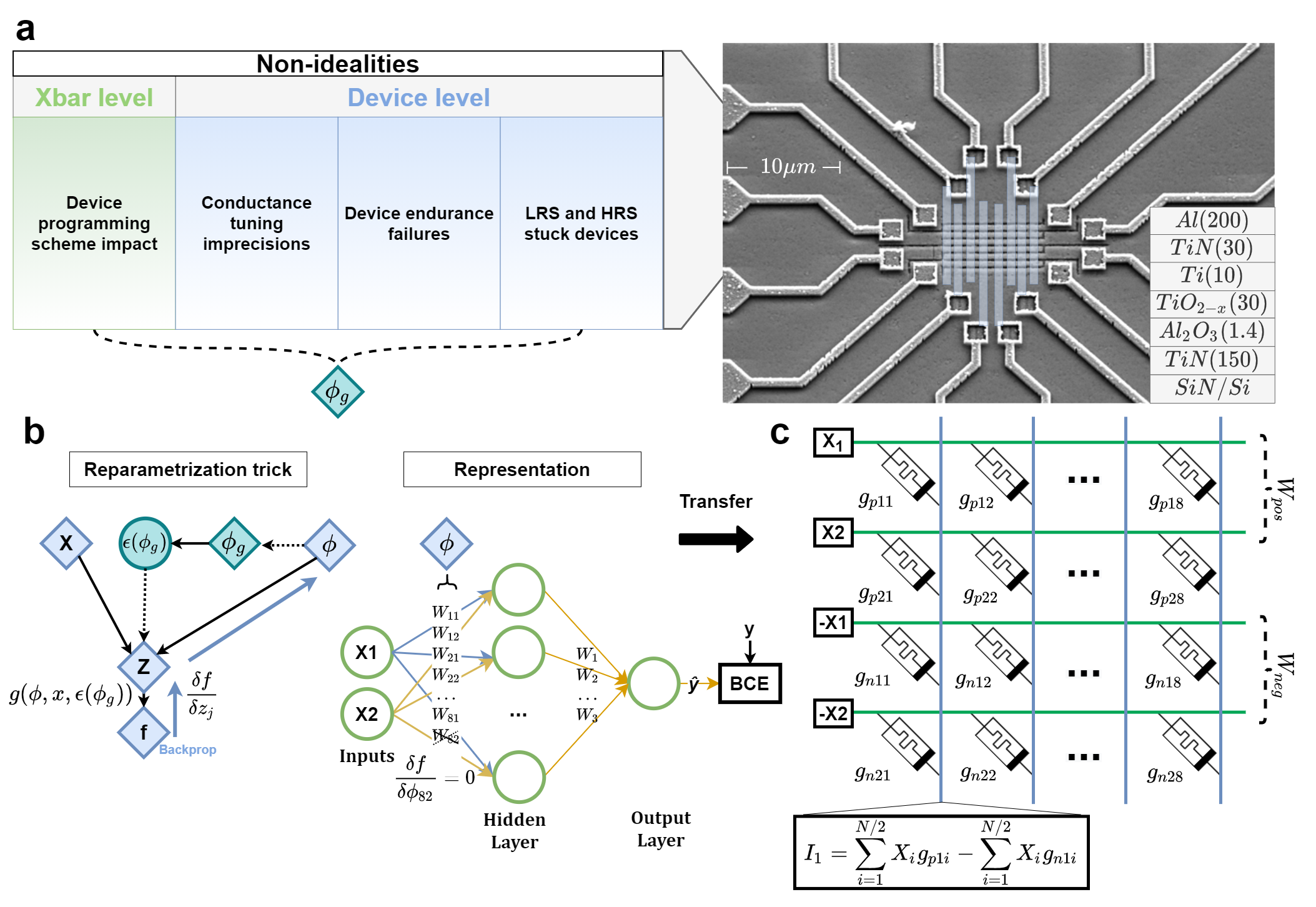
In this work, we report a novel hardware-aware ex-situ training approach that improves the robustness of neural network models against the non-idealities of -based memory crossbars. The main contributions of this study are the introduction of new, fully data-driven and computationally simple characterization and variability modeling methods that are used jointly with a reparametrization trick during training to mitigate precision losses when weights are converted into their equivalent ReRAM conductances on a passive crossbar. This procedure is often referred to as hardware-aware training. The simple variability models do not require computationally prohibitive mathematical and physical models, and they lead to good performance without requiring multiple rounds of tuning; these models require only reproducible characterizations that are all easy to automate. Figure 1 shows the overall hardware-aware procedure. The hardware-aware network provides accurate classification results for the half moons dataset for a much greater percentage of the simulated transfers compared to a regular neural network. This greater accuracy across transfers proves that the hardware-aware procedure is robust to significant biasing-scheme-effect conductance changes (up to 60 S), conductance tuning imprecision and neural network weights impacted by random substitutions to account for stuck devices. The devices studied in this work are 0T1R devices, and they can be seen in Figure 1 a and in Supplementary Figure 7.
Other works, such as zhou_bayesian_2021 ; Strukov-hardware-aware ; Mitigating-Imperfections , employ a similar approach. In zhou_bayesian_2021 , an impressive performance was reported but the authors chose not to consider device failures and only consider 1T1R devices, therefore neglecting biasing scheme effects. Meanwhile, Strukov-hardware-aware ; Mitigating-Imperfections deal with 0T1R passive crossbars and implement many different variability sources such as temperature, biasing scheme effect and non-linearity in their hardware simulations and training to great effect. However, the relationship between the variability and the crossbar position of the devices is not considered in these works. The focus is instead placed on a conductance tuning technique that mitigates biasing scheme disturbances. Also, the fact that our method depends solely on empirical data means that it is also applicable to different memristive technologies with slight modifications, rendering it highly adaptable. The biasing scheme considered in these other works is the V/2 scheme; the V/3 scheme is considered in this work and the variability modeling approaches are therefore different.
In this paper, we begin by explaining the different sources of variability that are taken into account by the hardware-aware network, along with the characterization process that led to the creation of each of these sources. We continue with a software demonstration that compares the performances of weights trained considering these variabilities and weights trained naively over 10,000 simulated ex-situ weight transfers for a simple binary classification problem. The hardware-aware network significantly outperforms the regular neural network.
II Results and discussion
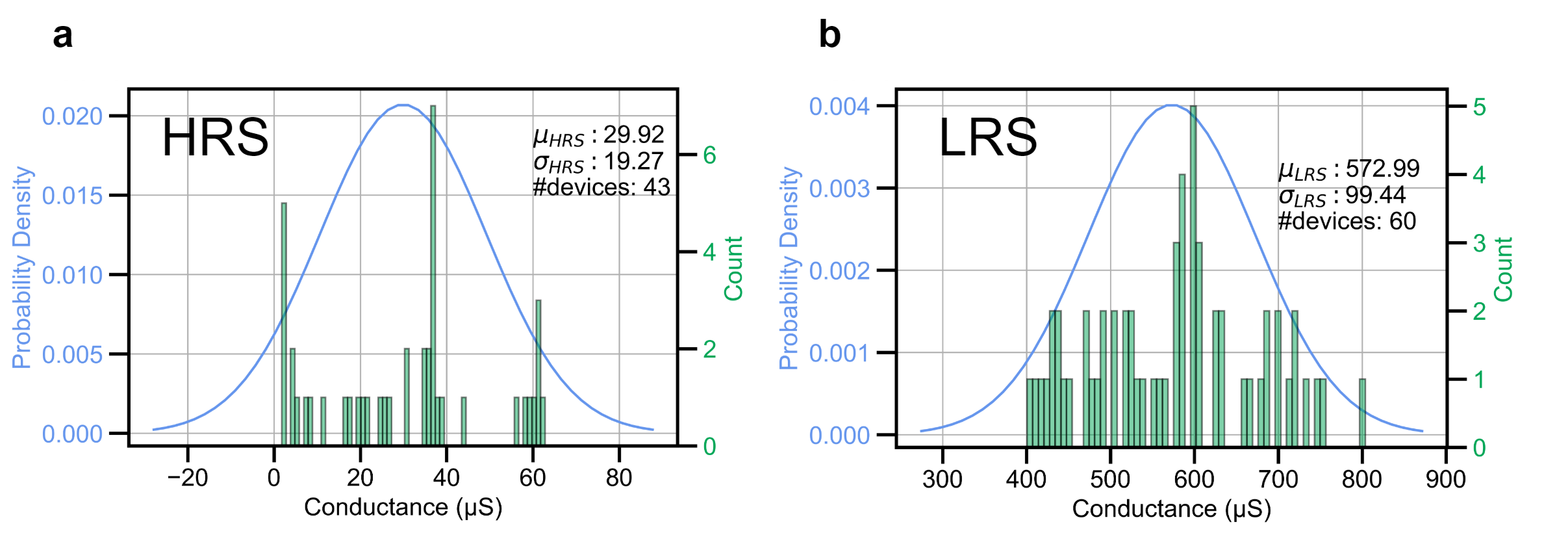
As previously mentioned, passive crossbars are afflicted by many different and often indirectly correlated non-idealities. The device-to-device and crossbar-to-crossbar variabilities are considerable and difficult to predict. Depending on a specific crossbar’s properties, a transferred neural network may perform well or very poorly. The proposed approach aims at using neural networks’ learning abilities to learn how to classify data points in spite of the effects that non-idealities will have on analog VMMs. These non-idealities were estimated through the extensive electrical characterization of TiO-based resistive memories fabricated in 88 crossbar and crosspoint configurations. The considered non-idealities were those deemed to have the greatest effect on VMMs, namely the conductance tuning imprecision, biasing scheme effects and high resistance state (HRS) and low resistance state (LRS) stuck devices.
During training, the neural network weights are converted from their software range to the predetermined mean achievable conductance range for every batch of data. The weights are then shifted according to randomized variability samples using a reparametrization trick https://doi.org/10.48550/arxiv.1312.6114 integrated into a modified version of the PyTorch library NEURIPS2019_9015 . The use of the reparametrization trick allows the Monte Carlo estimate of the expectation (every time we sample new weights) to be differentiable with respect to the weight parameters and enables backpropagation, as depicted in Figure 1b. The process is explained by the flowchart shown in Figure 1 and the mathematical details are given in Supplementary Note 1. All considered non-idealities are numerically added into a matrix created from the conversion of the network’s parameters to the conductance range and share the same dimensions. This matrix is converted back into the weight range after variabilities are added. The now-converted matrix is subtracted from the original parameter matrix to obtain the matrix used in the reparametrization trick. was determined to be from 100 S to 400 S by electrical characterizations made on our 88 crossbars mesoudy2021CMOS . The randomized variability samples depend on the conductance tuning imprecision and the biasing scheme effects recorded in a database. Percentages of neural network weights x and y corresponding to LRS and HRS stuck devices are also replaced by equivalent high or low conductance values. This effectively simulates the result of an ex-situ transfer on a crossbar, as depicted in Figure 1c, with randomized programming failures for every batch of training data. It also ensures that the network considers randomized potential sources of hardware-related errors. The trained network will converge towards the solution that is most robust to the average of all potential crossbars, considering our TiO memristive technology non-idealities.
The tests performed to gather the data in the non-ideality database used during training for tuning imprecision, biasing scheme effects and finally HRS or LRS stuck devices are described in the following subsections. In the case of the weight disturbances induced by the biasing scheme effect, fitting normal distributions to the data was unfortunately impossible. The Shapiro-Wilk tests for normality of the distributions fitted to the data usually returned an alpha value of less than 0.05, causing the null hypothesis to be rejected SHAPIRO1965 . A sample from this distribution does not approximate a recorded disturbance instance well. The approach taken instead was to sample a recorded conductance change from a portion of the database consisting of only raw data. This is different from sampling from a fitted distribution, which is done for the conductance tuning imprecision. In all of the tests, the conductance tuning procedure followed the pulse tuning technique presented in Alibart2012 with a 1% tuning tolerance.
Device conductance tuning imprecision
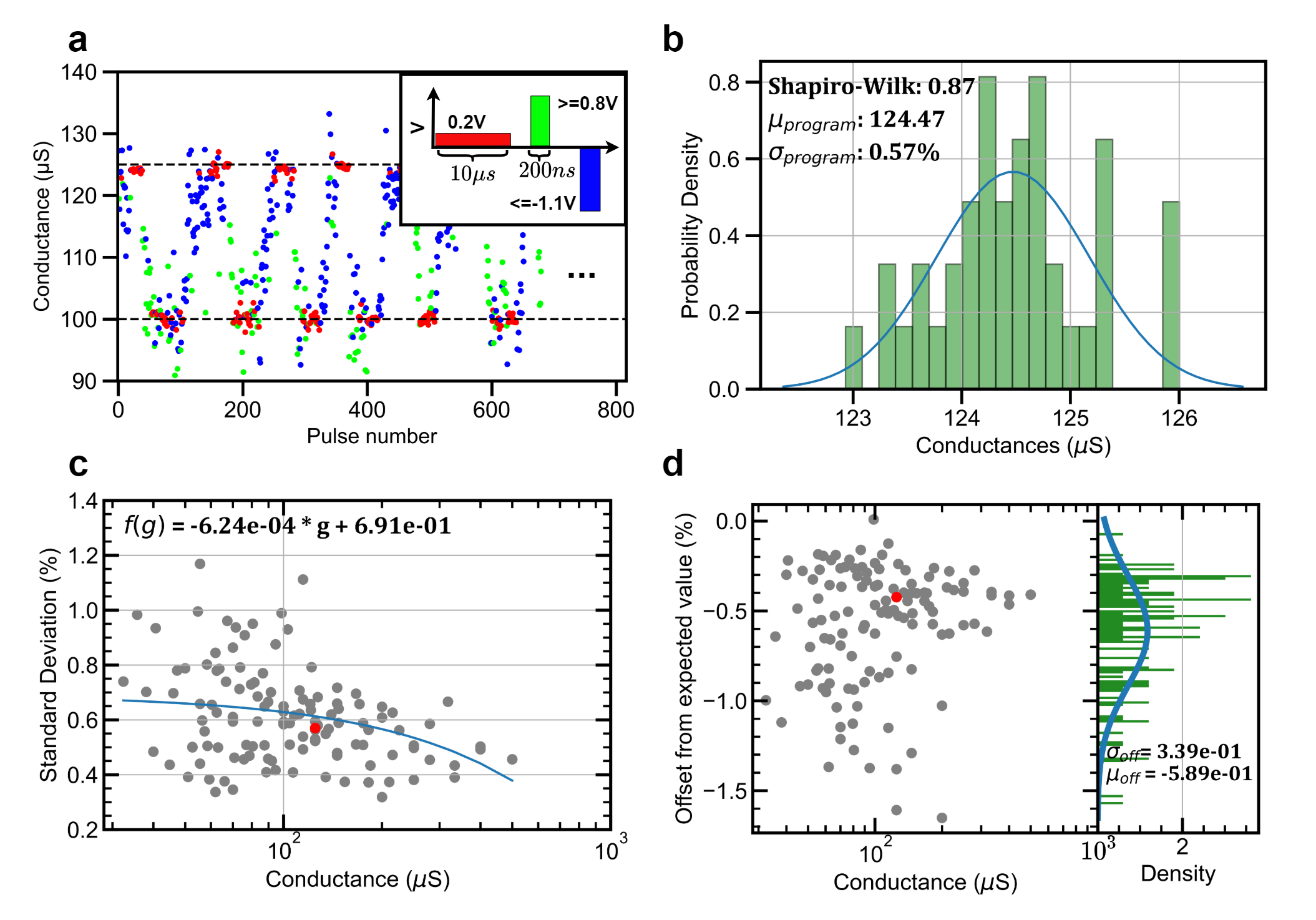
As shown in Figure 1a, the device-level conductance tuning imprecision is considered in the training process. The studies undertaken to characterize it were realized by dividing the achievable resistive ranges of all 29 studied devices into eight different equidistant levels and repeatedly performing a tuning/untuning procedure. Figure 2 illustrates how the statistical database was established, along with an example. Figure 2a shows the experimental data behind one instance of the procedure for a target conductance of 125 . The distribution of read values after the conductance reached and stabilized around the target conductance is shown in Figure 2b. This tuning/untuning procedure was repeated 40 times per level and per device. In Figure 2c and d, the data points corresponding to the data distribution in Figure 2b are depicted in red and are evaluated as follows:
| (1) |
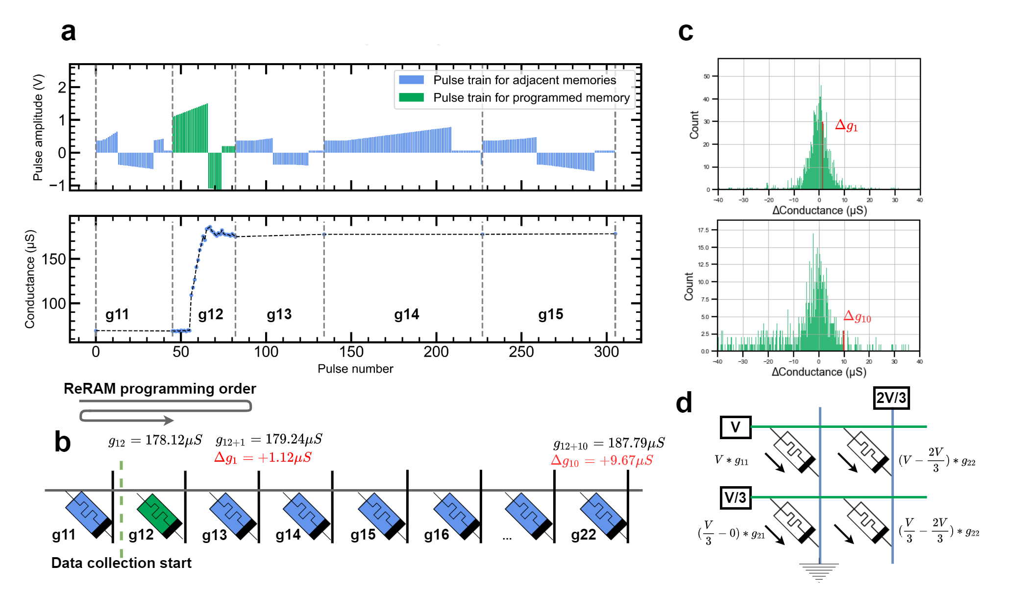
Figure 2c shows the standard deviation of the programing precision as a function of the conductance state of the devices tested, where the values are expressed in terms of a percentage of the desired conductance value, while Figure 2d shows the offset between the mean of the read conductance values after the tuning of the devices and their target conductance values. Since the devices are always tuned from a low conductive level to a high conductive level, the mean offset of the achieved conductance from the ideal target conductance is always negative. Therefore, the transfer on a crossbar should be performed after all devices are RESET in order to match this replicable offset, meaning that all devices should start from the off state.
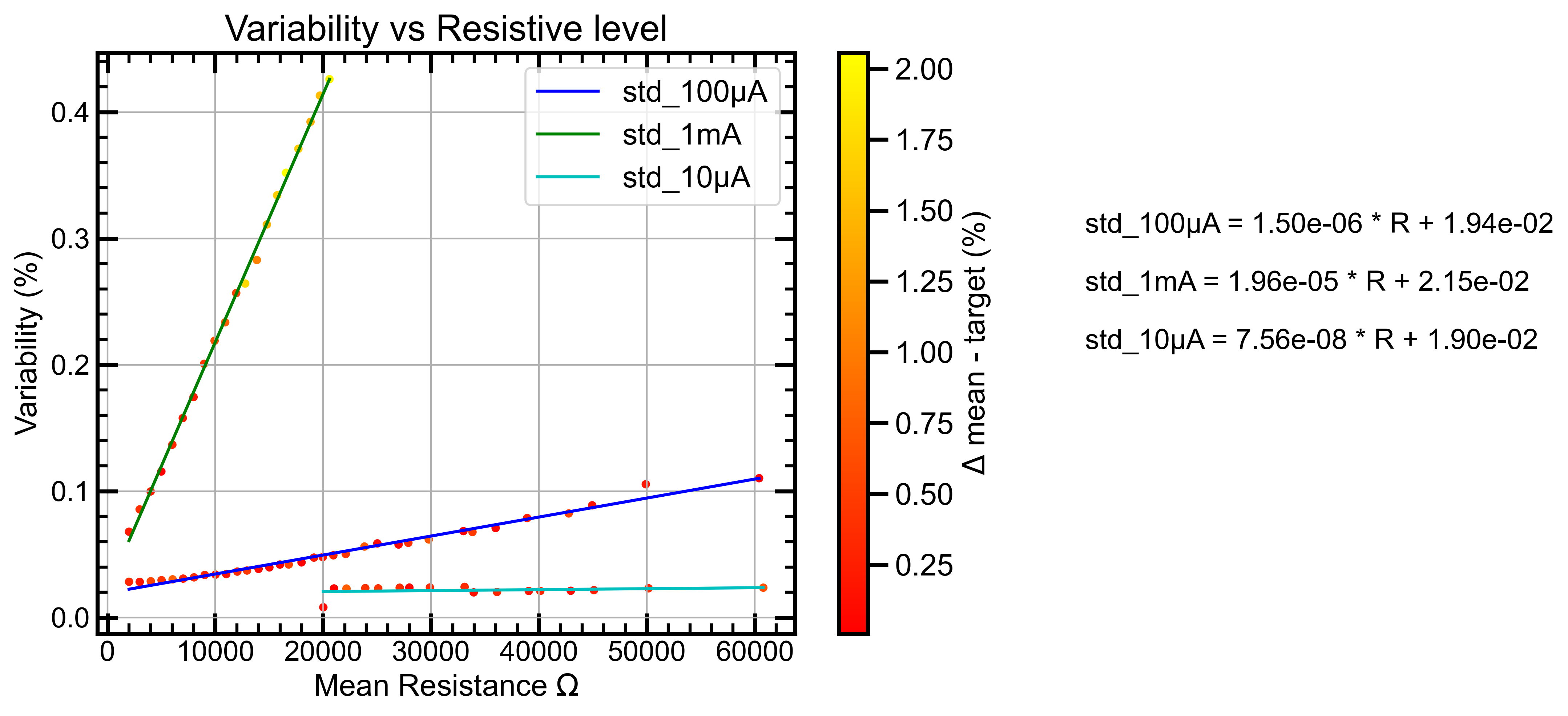
During training, when the network weights are transformed into software conductances and for signed weights or for unsigned weights, a weight is sampled from a normal distribution centered around these values with a standard deviation that depends on the conductive level of the transformed weight. Figure 2c shows the function defining this standard deviation relationship. This allows the network to take into account the correlation that is often observed between the conductive level and variability Dalgaty2021 . An offset is then sampled from a distribution , which is depicted in Figure 2d, and added to the sampled conductance value.
Because the test is performed by reading ten times before considering a memory to be programmed, the read variability on devices is also taken into account. An experiment was undertaken to isolate the read variability of the characterization equipment with respect to the variability of the measured values; it was found that the reading variability stemming from the instrument is one order of magnitude lower than that of the experimental data (Supplementary Figure 11.)
Conductance disturbances caused by biasing scheme effect
Programming devices on a passive crossbar require the use of a biasing scheme to reduce sneak path currents. The V/3 scheme was used in this study since all devices other than the addressed memory will see the same voltage of V/3. This standardizes and simplifies the process of adding variability to the weights. It also makes it possible to use higher-amplitude voltages to tune the devices without affecting neighboring devices significantly. In order to measure the change in the conductance of a device due to the programming of its neighbors, we tuned devices from three different crossbars, for a total of 144 devices (64 + 64 + 16), to random values within the expected conductance ranges . The disturbance of a device, after the tuning cycles for devices that are tuned after itself are complete, is recorded in the database. This disturbance is due to the V/3 biasing scheme. A thorough example is displayed in Figure
3a and b. The conductance changes caused by the biasing scheme accumulate through the crossbar programming, which can be observed by comparing the disturbance due to the programming of the neighbors of the device that is tuned first with that of the devices that are tuned last. As such, the database of recorded disturbance measurements is separated into sub-databases for each number of subsequent devices tuned after the programming of the current device. Figure 3c shows two such sub-databases, one for the scenario in which one additional device is tuned and one for the scenario in which ten additional devices are tuned. The device that is tuned last is the bottom-rightmost weight of our neural network matrix when it is transferred from top to bottom and left to right. It will see no conductance change due to the biasing scheme since it is the last-tuned device. The devices stuck in an HRS or LRS or that could not reach their target conductances were also not added in this database. If they had been included, the database would have been polluted by stuck or ineffective devices, which would have biased it towards no conductance change.
As can be seen in Figure 3c, a tail of recorded crosstalk effects is more prevalent for negative values. This is an indirect consequence of the asymmetrical device switching mechanism between the SET and RESET pulses. More negative pulses are required to reset devices than positive pulses. Thus, devices will, on average, see more successive negative pulses than positive pulses. This phenomenon is worsened by the fact that devices are individually affected differently by negative pulses, with more sensitive devices leading to greater conductance changes. A conductance change of up to 60 S was allowed in the sub-databases; this change is six times larger than the lowest possible conductance weight. The cases in which the disturbance is greater than this value usually correspond to an HRS or LRS failure.
During the training of the neural network, a random offset sampled from these sub-databases correlated to the positions of the weights in the crossbar is added to each weight. The use of the V/3 scheme, as shown in Figure 3d, makes it possible to proceed in this way. This ensures that the first weights in the matrices will see more V/3 amplitude pulses and will, on average, have a greater variability than the last devices that are programmed.
HRS-LRS stuck device substitution
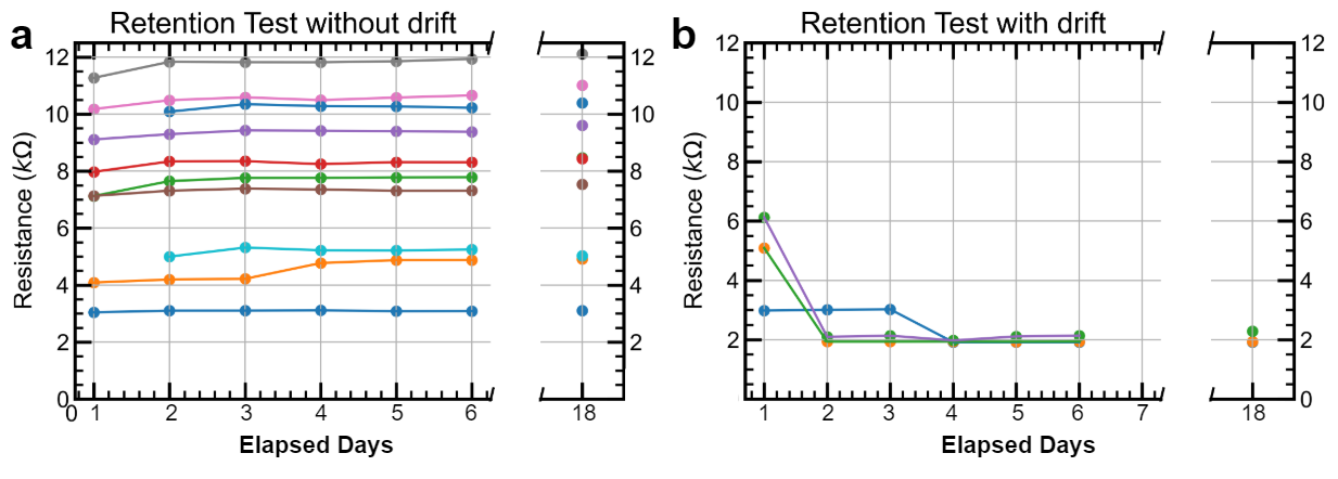
Some devices are stuck in a low or high resistive state due to defects. Regardless of the DC voltage or the pulse amplitudes that are applied to such devices, their conductive levels will never be tunable. As shown in Supplementary Figure 10, LRS failures include retention failures. Such failures are caused by temporal effects and cause the device conductance to drift over time to a typically higher conductance state. HRS failures may occur for devices that were not forming free or devices with a very narrow achievable conductance range lying outside the desired range. To account for these device faults, percentages of devices x and y corresponding to HRS and LRS stuck devices, respectively, have both positive () and negative () software weight components that are replaced by a randomly sampled failed device conductance. The percentages x and y are fixed throughout the training, but the affected weights are randomized for every batch of input data. This implies that certain weights will be doubly affected by this substitution if their positive and negative components are both assigned as failures.
The stuck devices’ conductances are sampled from two distributions based on the characterization of LRS and HRS stuck devices made on five 88 crossbars (320 devices). The conductance range of devices stuck in an HRS is much smaller than that of devices stuck in an LRS; HRS devices are defined as devices stuck below our HRS resistance of 100S. The distribution of failed HRS state devices can be seen in Figure 4a, while the distribution of failed LRS devices can be seen in Figure 4b. Since fitting the normal distribution is inappropriate for the HRS distribution, as it fails the Shapiro-Wilk normality test, HRS stuck device faults are uniformly sampled from the range [100 S, 10 S]. The impact of devices stuck below 10 S will be more negligible than the impact of those stuck at <100 S and >10 S. Indeed, devices stuck in a higher conductance state will have a greater impact on the summation of the currents during the analog matrix multiplication. Gradient descent is deactivated for the weights affected by HRS or LRS stuck weights. Typically, the fabrication yields of working devices on crossbars for state-of-the-art memristive devices are above 95% Bayat2018_95 , with some articles reporting near perfect crossbars with yields of 99% Kim2021 or even 100% 100yield . The percentages of HRS and LRS stuck devices should be chosen to reflect this fact. In fact, in general, the values of these parameters should be chosen as conservatively as possible so that the network converges to a solution that is robust to as many device failures as possible. Of course, replacing too many weights with random values at the extremities of the conductance range and therefore at the extremities of the overall weight range will prevent the network from converging to a solution, making the training impossible. This makes these percentage values tunable hyperparameters.
Mathematical expression
Overall, the mathematical equation representing the sampling of each of the devices for either positive or negative weight components is equation 2:
| (2) |
where is the direct conductance equivalent of the weight after a linear transformation between the two ranges (see Supplementary Note 1). The weight’s range is reevaluated for every batch during training since the maximum and minimum weight values are subject to change as the training progresses. is the sampled conductance tuning imprecision offset and is the sampled biasing scheme effect from programming adjacent devices with respect to the number of additional devices programmed after the current device. The variability associated with a device in training is dependent on both its target conductance level for both negative and positive weight components and the position of the devices in their respective crossbar. Every weight matrix is presumed to be programmed on a tiled crossbar or on a sub-section of a crossbar.
The network learns to expect more variability from the first devices that are programmed because of the biasing scheme effects and from devices at low conductance values and will adjust the importance of each weight accordingly. The substitution of random failed weights acts as a form of aggressive regularization, improving the network’s generalization. As can be expected, training a neural network with stochastic jumps in weight values leads to a longer training time compared to a regular neural network, as is the case for Bayesian neural networks. However, this constant sampling also enables the network to be more robust to overfitting watanabe_2009 .
Comparison with regular neural network
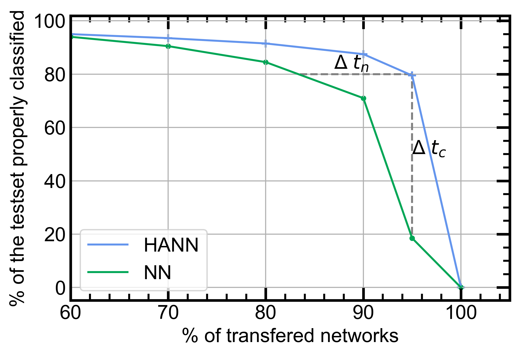
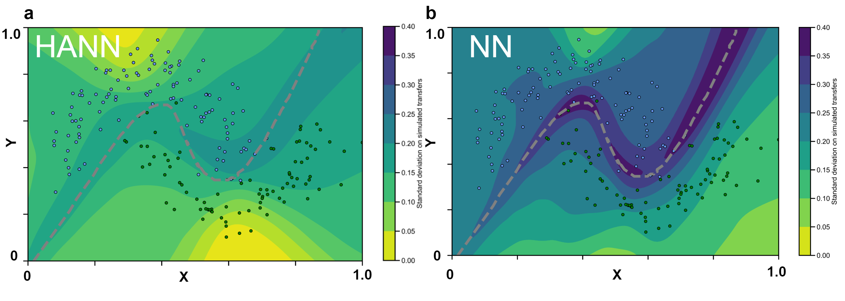
A simple half-moon problem was considered to compare the performance of our hardware-aware training approach with that of a regular neural network trained without taking into account hardware non-idealities. The two networks have the same learning rate of 0.01, and they use an Adam optimizer ADAM with a momentum of 0.9. The batch size used was 256. A neural network with one hidden layer with eight neurons is considered, and the sigmoid activation function is used (as depicted in Figure 1b). The cost function used is the binary cross-entropy loss Aldrich1997 . During training, hyperparameter values of 0.5% were chosen for both the LRS-stuck and HRS-stuck substitutions. For the first layer, a recorded average of 3.1% of neural network weights were affected by random substitutions of LRS and HRS stuck devices during training. A half-moon classification problem training set of 875 data points and a test set of 200 data points were randomly generated. The neural network (NN) is trained without any consideration of the variability and then evaluated with the stochastic effects added to compare its performance to that of the hardware-aware NN (HANN). This is repeated n times to determine what percentage of the test set could be classified well over a given percentage of the n simulated transferred networks. These results are expressed in Table 1 in Supplementary Note 4. A comparison of the accuracies is also displayed in Figure 5. Interpreting these results, we see that 79.5% of the test set can be properly classified by at least 95% of the simulated transferred hardware-aware networks. On the other hand, only 18.5% of the test set can be properly classified by at least 95% of the simulated transferred regular neural networks. We observe that 87.5% of the test set can be properly classified by at least 90% of the simulated transferred hardware-aware networks, while 71% of the test set can be properly classified by at least 90% of the regular networks. The hardware-aware neural network training techniques contribute significantly to maintaining a high consistency and accuracy between simulated transferred networks. Figure 6 offers a graphical interpretation of the difference in the relative variability by showing the results of the test set classifications over 1,000 simulated transfers for each of the two networks, along with a heatmap representation of the variability with respect to the entire data space for the half moons dataset. Note that this is for a single instance of a hardware-aware-trained NN and a regularly trained NN. The variability, depicted by a deeper blue, is greater for the regular neural network and, as expected, is also greater at the frontier between the two classes.
III Conclusion
It was demonstrated in this paper that the use of hardware-aware training techniques can make neural networks significantly more robust to their often difficult transfer onto passive crossbar arrays. This protocol integrates experimentally measured non-idealities such as the conductance tuning imprecision, biasing scheme effects and device failures into the neural network training.
A classification task using the half moons dataset reveals that our hardware-aware training protocol results in a 95% accuracy across simulated transfers for 79.5% of the test set, compared to only 18.5% for the regular neural network. The hardware-aware training procedure could enable the use of passive crossbars despite their non-idealities for inference tasks and proposes a parallel solution to the usual fabrication process improvements. It may serve as a middle ground between fabrication and software solutions to accelerate practical, real-life applications of memristive devices. Furthermore, setting up a custom hardware-aware neural network architecture using preexisting libraries proves to be relatively straightforward and inexpensive in terms of hardware.
While the devices studied here are TiO passive crossbars, techniques like this are applicable to different memristive technologies as long as a new database is built using the same procedures presented in this article. A future study should focus on evaluating the scalability of this approach, with respect to the advantages (robustness, accuracy) and disadvantages (training time, variability-induced local minima). The potential of using this technique for more complex datasets should also be evaluated. Faster convergence during training could most likely be achieved by integrating the variability into the gradient descent procedure. This model could be improved by adding additional variability sources and by developing versatile libraries that make hardware non-idealities compatible with neural network requirements. The philosophy behind this work is to realistically render compatible in-memory computing for neural networks with the current non-negligible hardware non-idealities present in passive crossbar arrays. This demonstration, based on experimental data, is a step forward in making the use of passive crossbars for neural network matrix-vector multiplications viable in spite of their inherent shortcomings.
Methods
Tuning algorithm and characterization details
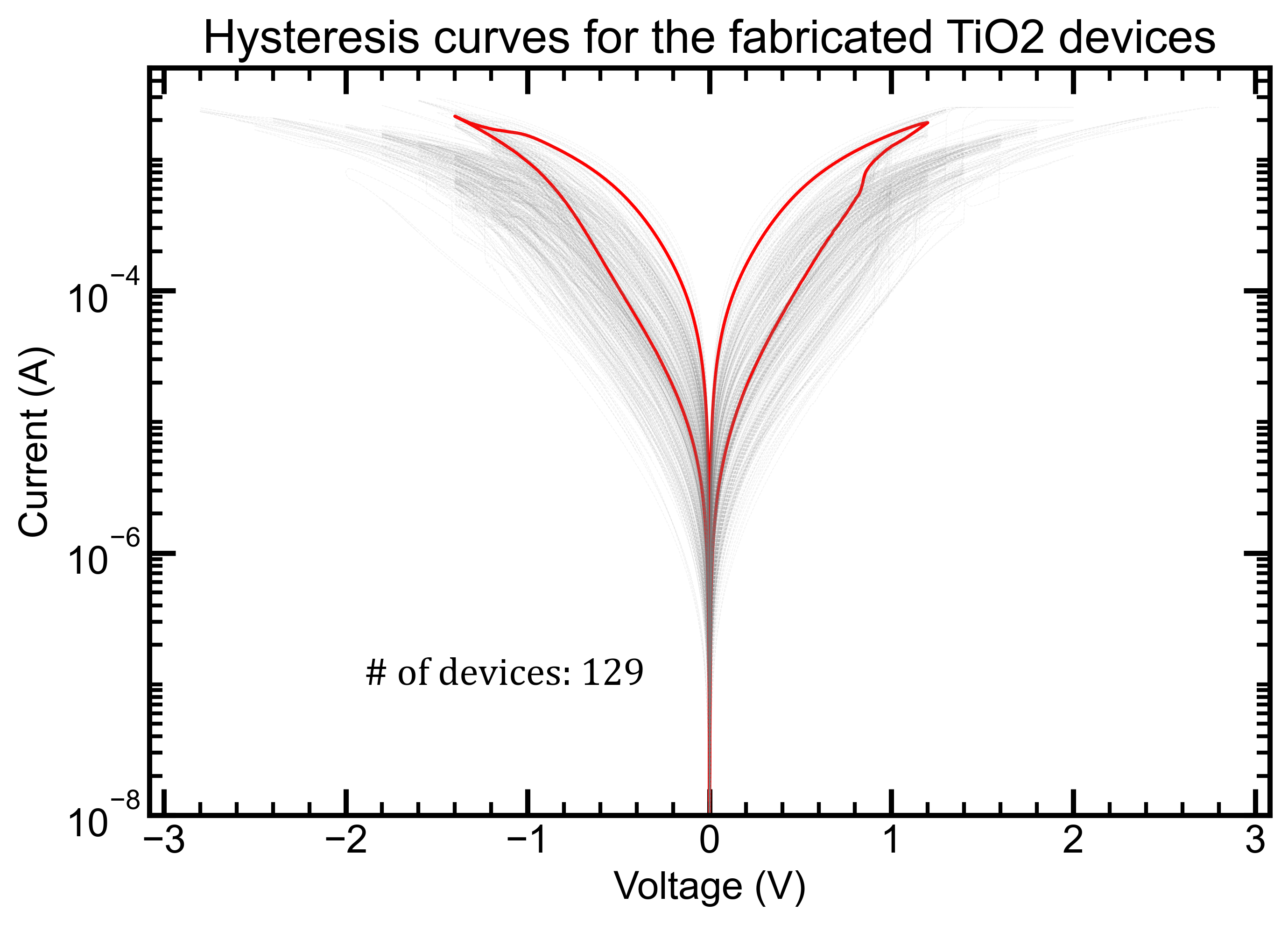
The pulse tuning algorithm presented in Alibart2012 was used. A memory was considered programmed when ten successive reading pulses returned a value within a tolerance around the target. The writing pulses were incremented from [0.8 V, 2 V] for SET pulses and from [-1.1 V, -2.4 V] for RESET pulses and had a duration of 200 ns. The read pulses had a duration of 10 s and an amplitude of 0.2 V, while the current measurement range was 100 A. The devices considered were forming free. Figure 2a depicts the conductance evolution using the pulse conductance tuning procedure. Devices that failed before the completion of the testing procedure were kept in the database, as this corresponds to a realistic scenario of a device’s behavior before imminent failure, while devices that failed before testing began were kept in the HRS-stuck or LRS-stuck databases. More information regarding the characterization setup can be found in Supplementary Figure 8 and Supplementary Note 2. A graph of hysteresis curves under DC stimulation for 129 of our devices is also available in Supplementary Figure 9.
Fabrication of CMOS-compatible TiO-based memristor crossbar
The samples used for measurements were prepared as described in a previous publication mesoudy2021CMOS . First, a 600-nm-thick SiN layer was deposited on a Si substrate using low-pressure chemical vapor deposition (LPCVD). Electron-beam lithography (EBL) was used to pattern 400-nm-wide bottom electrodes, which were etched 150 nm deep using an inductively coupled plasma etching process with CF4/He/H2 chemistry. The trenches were filled with 600-nm-thick TiN, deposited by reactive sputtering, and polished using chemical-mechanical polishing (CMP) to remove the excess TiN and planarize the samples. This resulted in embedded TiN electrodes within the SiN layer. The active switching layer was composed of 1.5 nm of Al2O3 and 15 nm of TiO2, which were deposited using atomic layer deposition and reactive sputtering, respectively. EBL and plasma etching with BCl3/Cl2/Ar chemistry were used to deposit and pattern 400-nm-wide top electrode lines with Ti (10 nm)/TiN (30 nm)/Al (200 nm). The switching layer outside the crossbar region was etched using the same process to suppress line-to-line leakages and open the ends of bottom electrodes. The crossbars were then encapsulated within a 500-nm-thick PECVD SiO2 layer, and the contacts on the open ends of the top and bottom electrodes were etched using plasma etching with CF4/He/H2 chemistry. Ti (10 nm)/Al (400 nm) contact pads for wiring were deposited and patterned using EBL and plasma etching with BCl3/Cl2/Ar chemistry. Finally, the sample was subjected to a rapid thermal annealing process at 350∘C in N2 gas for an unspecified duration.
Data availability
The hardware-aware training library, along with some of the experimental data, can be found in a GitHub repository that has been made publicly available at DroletHARDWAREAWARE . The rest of the data that support this work are available from the corresponding author upon reasonable request.
Acknowledgements
This work was supported by the Natural Sciences and Engineering Research Council of Canada (NSERC) and by the Fonds de Recherche du Québec Nature et Technologie (FRQNT). We acknowledge financial support from the EU: ERC-2017-COG project IONOS (# GA 773228). We would like to acknowledge Jonathan Vermette, Vincent-Philippe Rhéaume and the LCSM and LNN cleanroom staff for their assistance with the electrical characterization setup and nanofabrication process development. LN2 is a joint International Research Laboratory (IRL 3463) funded and co-operated in Canada by Université de Sherbrooke (UdeS) and in France by CNRS as well as ECL, INSA Lyon, and Université Grenoble Alpes (UGA). It is also supported by the Fonds de Recherche du Québec Nature et Technologie (FRQNT). We would also like to thank the IEMN cleanroom engineers for their help with the device fabrication.
Author contributions
P.D. performed most of the experiments, designed the neural networks, analyzed and post-processed the measurements and created the characterization setup. V.Y. helped in designing the neural network architecture. P.A.M. contributed to the experimental setup and along with M.V. helped with the characterization. R.D., J.A.Z, P.G., S.E. and M.V. fabricated the memristor devices. Y.B., F.A., S.E., S.W. and D.D supervised the project. P.D. wrote the manuscript with input from all of the authors.
Competing interests
The authors declare no competing interests.
References
- (1) Z. Zhou, X. Chen, E. Li, L. Zeng, K. Luo, and J. Zhang, “Edge intelligence: Paving the last mile of artificial intelligence with edge computing,” Proceedings of the IEEE, vol. 107, no. 8, pp. 1738–1762, 2019.
- (2) H. Li, B. Gao, Z. Chen, Y. Zhao, P. Huang, H. Ye, L. Liu, X. Liu, and J. Kang, “A learnable parallel processing architecture towards unity of memory and computing,” Scientific Reports, vol. 5, no. 1, Aug. 2015. [Online]. Available: https://doi.org/10.1038/srep13330
- (3) A. Amirsoleimani, F. Alibart, V. Yon, J. Xu, M. R. Pazhouhandeh, S. Ecoffey, Y. Beilliard, R. Genov, and D. Drouin, “In-memory vector matrix multiplication in monolithic complementary metal–oxide–semiconductor-memristor integrated circuits: Design choices, challenges, and perspectives,” Advanced Intelligent Systems, vol. 2, no. 11, p. 2000115, Aug. 2020. [Online]. Available: https://doi.org/10.1002/aisy.202000115
- (4) D. S. Jeong, K. M. Kim, S. Kim, B. J. Choi, and C. S. Hwang, “Memristors for energy-efficient new computing paradigms,” Advanced Electronic Materials, vol. 2, no. 9, p. 1600090, Aug. 2016. [Online]. Available: https://doi.org/10.1002/aelm.201600090
- (5) D. Ielmini and G. Pedretti, “Device and circuit architectures for in-memory computing,” Advanced Intelligent Systems, vol. 2, no. 7, p. 2000040, May 2020. [Online]. Available: https://doi.org/10.1002/aisy.202000040
- (6) A. E. Mesoudy, G. Lamri, R. Dawant, J. Arias-Zapata, P. Gliech, Y. Beilliard, S. Ecoffey, A. Ruediger, F. Alibart, and D. Drouin, “Fully CMOS-compatible passive TiO2-based memristor crossbars for in-memory computing,” Microelectronic Engineering, vol. 255, p. 111706, Feb. 2022. [Online]. Available: https://doi.org/10.1016/j.mee.2021.111706
- (7) T. Dalgaty, E. Esmanhotto, N. Castellani, D. Querlioz, and E. Vianello, “Ex situ transfer of Bayesian neural networks to resistive memory-based inference hardware,” Advanced Intelligent Systems, vol. 3, no. 8, p. 2000103, May 2021. [Online]. Available: https://doi.org/10.1002/aisy.202000103
- (8) H. Kim, M. R. Mahmoodi, H. Nili, and D. B. Strukov, “4k-memristor analog-grade passive crossbar circuit,” Nature Communications, vol. 12, no. 1, Aug. 2021. [Online]. Available: https://doi.org/10.1038/s41467-021-25455-0
- (9) F. M. Bayat, M. Prezioso, B. Chakrabarti, H. Nili, I. Kataeva, and D. Strukov, “Implementation of multilayer perceptron network with highly uniform passive memristive crossbar circuits,” Nature Communications, vol. 9, no. 1, Jun. 2018. [Online]. Available: https://doi.org/10.1038/s41467-018-04482-4
- (10) D. Kau, S. Tang, I. Karpov, R. Dodge, B. Klehn, J. Kalb, J. Strand, A. Diaz, N. Leung, J. Wu, S. Lee, T. Langtry, K.-W. Chang, C. Papagianni, J. Lee, J. Hirst, S. Erra, E. Flores, N. Righos, and G. Spadini, “A stackable cross point phase change memory,” Jan. 2010, pp. 1–4.
- (11) Y. Nishitani, Y. Kaneko, M. Ueda, T. Morie, and E. Fujii, “Three-terminal ferroelectric synapse device with concurrent learning function for artificial neural networks,” Journal of Applied Physics, vol. 111, no. 12, p. 124108, Jun. 2012. [Online]. Available: https://doi.org/10.1063/1.4729915
- (12) H. Nikam, S. Satyam, and S. Sahay, “Long short-term memory implementation exploiting passive RRAM crossbar array,” IEEE Transactions on Electron Devices, vol. 69, no. 4, pp. 1743–1751, 2022.
- (13) J. Han, H. Liu, M. Wang, Z. Li, and Y. Zhang, “ERA-LSTM: An efficient ReRam-based architecture for long short-term memory,” IEEE Transactions on Parallel and Distributed Systems, vol. PP, pp. 1–1, 12 2019.
- (14) W. Chen, Z. Qi, Z. Akhtar, and K. Siddique, “Resistive-RAM-based in-memory computing for neural network: A review,” Electronics, vol. 11, no. 22, p. 3667, Nov. 2022. [Online]. Available: https://doi.org/10.3390/electronics11223667
- (15) Y. Lin, Q. Zhang, J. Tang, B. Gao, C. Li, P. Yao, Z. Liu, J. Zhu, J. Lu, X. S. Hu, H. Qian, and H. Wu, “Bayesian neural network realization by exploiting inherent stochastic characteristics of analog RRAM,” in 2019 IEEE International Electron Devices Meeting (IEDM), 2019, pp. 14.6.1–14.6.4.
- (16) Y. Zhou, X. Hu, L. Wang, and S. Duan, “Bayesian neural network enhancing reliability against conductance drift for memristor neural networks,” Sci. China Inf. Sci., vol. 64, no. 6, p. 160408, Jun. 2021. [Online]. Available: https://link.springer.com/10.1007/s11432-020-3204-y
- (17) A. Malhotra, S. Lu, K. Yang, and A. Sengupta, “Exploiting oxide based resistive RAM variability for Bayesian neural network hardware design,” IEEE Transactions on Nanotechnology, vol. 19, pp. 328–331, 2020.
- (18) F. Alibart, E. Zamanidoost, and D. B. Strukov, “Pattern classification by memristive crossbar circuits using ex situ and in situ training,” Nature Communications, vol. 4, no. 1, Jun. 2013. [Online]. Available: https://doi.org/10.1038/ncomms3072
- (19) C.-X. Xue, T.-Y. Huang, J.-S. Liu, T.-W. Chang, H.-Y. Kao, J.-H. Wang, T.-W. Liu, S.-Y. Wei, S.-P. Huang, W.-C. Wei, Y.-R. Chen, T.-H. Hsu, Y.-K. Chen, Y.-C. Lo, T.-H. Wen, C.-C. Lo, R.-S. Liu, C.-C. Hsieh, K.-T. Tang, and M.-F. Chang, “15.4A 22nm 2Mb ReRAM compute-in-memory macro with 121-28TOPS/W for multibit MAC computing for tiny AI edge devices,” 2020 IEEE International Solid- State Circuits Conference (ISSCC), pp. 244–246, 2020.
- (20) P. Yao, H. Wu, B. Gao, S. B. Eryilmaz, X. Huang, W. Zhang, Q. Zhang, N. Deng, L. Shi, H.-S. P. Wong, and H. Qian, “Face classification using electronic synapses,” Nature Communications, vol. 8, no. 1, May 2017. [Online]. Available: https://doi.org/10.1038/ncomms15199
- (21) Q. Xia and J. J. Yang, “Memristive crossbar arrays for brain-inspired computing,” Nature Materials, vol. 18, no. 4, pp. 309–323, Mar. 2019. [Online]. Available: https://doi.org/10.1038/s41563-019-0291-x
- (22) S. Ambrogio, S. Balatti, A. Cubeta, A. Calderoni, N. Ramaswamy, and D. Ielmini, “Understanding switching variability and random telegraph noise in resistive RAM,” in 2013 IEEE International Electron Devices Meeting, 2013, pp. 31.5.1–31.5.4. [Online]. Available: https://doi.org/10.1109/IEDM.2013.6724732
- (23) V. Yon, A. Amirsoleimani, F. Alibart, R. G. Melko, D. Drouin, and Y. Beilliard, “Exploiting non-idealities of resistive switching memories for efficient machine learning,” Frontiers in Electronics, vol. 3, Mar. 2022. [Online]. Available: https://doi.org/10.3389/felec.2022.825077
- (24) Z. Fahimi, M. R. Mahmoodi, M. Klachko, H. Nili, and D. B. Strukov, “The impact of device uniformity on functionality of analog passively-integrated memristive circuits,” IEEE Transactions on Circuits and Systems I: Regular Papers, vol. 68, no. 10, pp. 4090–4101, 2021.
- (25) Z. Fahimi, M. R. Mahmoodi, M. Klachko, H. Nili, H. Kim, and D. B. Strukov, “Mitigating imperfections in mixed-signal neuromorphic circuits,” 2021. [Online]. Available: https://arxiv.org/abs/2107.04236
- (26) D. P. Kingma and M. Welling, “Auto-encoding variational Bayes,” 2013. [Online]. Available: https://arxiv.org/abs/1312.6114
- (27) A. Paszke, S. Gross, F. Massa, A. Lerer, J. Bradbury, G. Chanan, T. Killeen, Z. Lin, N. Gimelshein, L. Antiga, A. Desmaison, A. Kopf, E. Yang, Z. DeVito, M. Raison, A. Tejani, S. Chilamkurthy, B. Steiner, L. Fang, J. Bai, and S. Chintala, “Pytorch: An imperative style, high-performance deep learning library,” in Advances in Neural Information Processing Systems 32. Curran Associates, Inc., 2019, pp. 8024–8035. [Online]. Available: http://papers.neurips.cc/paper/9015-pytorch-an-imperative-style-high-performance-deep-learning-library.pdf
- (28) S. S. Shapiro and M. B. Wilk, “An analysis of variance test for normality (complete samples),” Biometrika, vol. 52, no. 3-4, pp. 591–611, Dec. 1965. [Online]. Available: https://doi.org/10.1093/biomet/52.3-4.591
- (29) F. Alibart, L. Gao, B. D. Hoskins, and D. B. Strukov, “High precision tuning of state for memristive devices by adaptable variation-tolerant algorithm,” Nanotechnology, vol. 23, no. 7, p. 075201, Jan. 2012. [Online]. Available: https://doi.org/10.1088/0957-4484/23/7/075201
- (30) F. M. Bayat, M. Prezioso, B. Chakrabarti, H. Nili, I. Kataeva, and D. Strukov, “Implementation of multilayer perceptron network with highly uniform passive memristive crossbar circuits,” Nature Communications, vol. 9, no. 1, Jun. 2018. [Online]. Available: https://doi.org/10.1038/s41467-018-04482-4
- (31) G. C. Adam, B. D. Hoskins, M. Prezioso, F. Merrikh-Bayat, B. Chakrabarti, and D. B. Strukov, “3-D memristor crossbars for analog and neuromorphic computing applications,” IEEE Transactions on Electron Devices, vol. 64, no. 1, pp. 312–318, 2017.
- (32) S. Watanabe, Algebraic Geometry and Statistical Learning Theory, ser. Cambridge Monographs on Applied and Computational Mathematics. Cambridge University Press, 2009.
- (33) D. P. Kingma and J. Ba, “Adam: A method for stochastic optimization,” 2014. [Online]. Available: https://arxiv.org/abs/1412.6980
- (34) J. Aldrich, “R.A. Fisher and the making of maximum likelihood 1912-1922,” Statistical Science, vol. 12, no. 3, Sep. 1997. [Online]. Available: https://doi.org/10.1214/ss/1030037906
- (35) P. Drolet and V. Yon, “Hardware-aware article library,” https://github.com/3it-nano/Hardware-Aware-Article, 2023.
- (36) P.-A. Mouny, “B1530a control script,” https://github.com/3it-nano/B1530A_control, 2021.
Supplementary Materials
Supplementary Note 1: Mathematical expression of range conversions between weights and conductances
The following equations represent the conversion of the weights to the conductance range, the addition of the noise from the reparametrization trick and the conversion back to the initial weight range. In these equations, is the minimal weight value, is the maximal weight value and is the maximal absolute value of the weights. S and S, as described previously in this article. As shown in equation 3, the weights are separated into negative and positive components, with all weight components of the opposite sign being set to 0 and negative weight values being converted into positive values. The weights are then converted through min-max scaling to the conductance range, as shown in equation 4. An epsilon parameter that depends on the obtained positive and negative component conductance values is added to the weights, which are then converted back into the initial range, as shown in equation 6. The value of the final parameter for the reparametrization trick, as shown in Figure 1b, is therefore represented by equation 7:
| (3) |
| (4) |
| (5) |
| (6) |
| (7) |
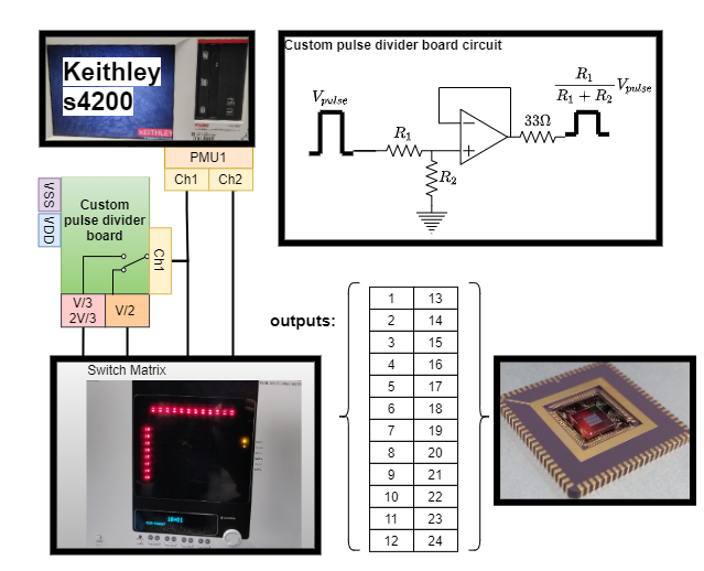
Supplementary Note 2: Electrical characterizations The electrical characterizations performed for the conductance tuning experiments were carried out with a Keysight B1500 parameter analyzer. The waveform generator/fast measurement unit (WGFMU) module was used, along with a custom C++ script based on a Keysight library MounyB15002021 . The instruments were controlled through a GPIB-USB connection. The crossbar programming and characterization were performed using a Keithley S4200 system attached to a custom pulse divider PCB and connected to a Keithley 707B switch matrix. The signals were then multiplexed onto a wire-bonded chip resting on another printed circuit board (PCB) platform, as depicted in Supplementary Figure 8. A custom C library was created to be used with the KULT, KITE and KCON software suite on the Keithley.
Supplementary Note 3: Comparative table of the results of the neural networks
|
|
|
||||||||
|---|---|---|---|---|---|---|---|---|---|---|
| 100 | 0 | 0 | ||||||||
| 95 x <100 | 37 (18.5%) | 159 (79.5%) | ||||||||
| 90 x <95 | 105 (52.5%) | 16 (8%) | ||||||||
| 80 x <90 | 27 (13.5%) | 8 (4%) | ||||||||
| 70 x <80 | 12 (6%) | 4 (2%) | ||||||||
| 60 x <70 | 7 (3.5%) | 3 (1.5%) | ||||||||
| 50 x <60 | 6 (3%) | 2 (1%) | ||||||||
| x 50 | 6 (3%) | 8 (4%) | ||||||||
| Total | 200 (100%) | 200 (100%) |