Ab initio investigation of the crystallization mechanism of cadmium selenide
Abstract
Cadmium selenide (CdSe) is an inorganic semiconductor with unique optical and electronic properties that made it useful in various applications, including solar cells, light-emitting diodes, and biofluorescent tagging. In order to synthesize high-quality crystals and subsequently integrate them into devices, it is crucial to understand the atomic scale crystallization mechanism of CdSe. Unfortunately, such studies are still absent in the literature. To overcome this limitation, we employed an enhanced sampling-accelerated active learning approach to construct a deep neural potential with ab initio accuracy for studying the crystallization of CdSe. Our brute-force molecular dynamics simulations revealed that a spherical-like nucleus formed spontaneously and stochastically, resulting in a stacking disordered structure where the competition between hexagonal wurtzite and cubic zinc blende polymorphs is temperature-dependent. We found that pure hexagonal crystal can only be obtained approximately above 1430 K, which is 35 K below its melting temperature. Furthermore, we observed that the solidification dynamics of Cd and Se atoms were distinct due to their different diffusion coefficients. The solidification process was initiated by lower mobile Se atoms forming tetrahedral frameworks, followed by Cd atoms occupying these tetrahedral centers and settling down until the third-shell neighbor of Se atoms sited on their lattice positions. Therefore, the medium-range ordering of Se atoms governs the crystallization process of CdSe. Our findings indicate that understanding the complex dynamical process is the key to comprehending the crystallization mechanism of compounds like CdSe, and can shed lights in the synthesis of high-quality crystals.
keywords:
Crystallization mechanism, Cadmium selenide, Neural network potential, Molecular dynamics simulation[label1]organization=State Key Laboratory of Solidification Processing, International Center for Materials Discovery, School of Materials Science and Engineering, Northwestern Polytechnical University, city=Xi’an, postcode=710072, country=China \affiliation[label2]organization=Italian Institute of Technology, addressline=Via E. Melen 83, city=Genoa, postcode=16152, country=Italy
1 Introduction
Cadmium selenide (CdSe) is a binary chalcogenide compound that has garnered extensive attention due to its unique nonlinear optical and wave absorbing properties [1, 2, 3, 4]. When confined to the nanoscale, CdSe exhibits tunable quantum confinement effects, and its quantum dots have been utilized in a broad range of applications, including solar cells [5, 6], light-emitting diodes [7, 8], and biofluorescent tagging [9, 10]. In practical applications, a high-quality CdSe crystal with uniform properties is desired. However, synthesizing CdSe crystals is challenging due to their high melting temperature and high vapour pressure [11]. For its bulk phase, supercooling not far from the melting temperature is usually adopted in the Bridgman method to obtain a pure single crystal [12, 13]. While for its nanoscale form, CdSe mainly crystallizes into a stacking disordered structure in a solution at relatively low temperature [14, 15]. Therefore, understanding the crystallization process of CdSe is essential to control and improve the quality and subsequently integrate it into more complex systems and advanced devices.
At ambient pressure, CdSe crystallizes into two different phases, namely hexagonal wurtzite (WZ) and cubic zinc blende (ZB) [16, 17], which are arranged in the order of ABAB… and ABCABC… sequence along the z-axis, respectively (see Fig. S1). Both structures feature a tetrahedral diamond lattice network, one of the most ubiquitous structural prototypes [18]. Understanding the crystallization process of the diamond lattice-based structure has attracted extensive attention in the literature from the crystallization of silicon [19] to the homogeneous nucleation of ice and silica [20, 21, 22]. However, to the best of our knowledge, studies on the nucleation process of two-component based diamond lattice structures, such as CdSe, are still absent in the literature. It is difficult to imagine how these two types of elements, i.e., Cd and Se, interact with each other and crystallize into a diamond lattice.
Molecular dynamics (MD) is a powerful methodology to simulate the crystallization process of CdSe but is fraught with great challenges from several perspectives. For one thing, as a binary chalcogenide semiconductor compound, CdSe has both ionic and covalent characteristics [23, 24], and chemical bonding changes need an accurate description of the atomic interaction. In addition, the ground state energy of cubic ZB phase is only 0.9 meV/atom lower than that of the hexagonal WZ phase based on first-principles calculations, while at relatively high temperatures the hexagonal phase is more stable [25]. In addition, the [001] face of hexagonal phase is indistinguishable from the [111] face of cubic phase, and a stacking disordered structure consisting of staggered layers of these two phases is formed easily. Thus, the subtle difference between the hexagonal and cubic structures needs to be described accurately. Ab initio MD (AIMD) is, in principle, a good solution to overcome these challenges. However, the high computational cost makes it prohibitive to perform large-scale and long simulations, which are essential to study the nucleation and growth processes of CdSe.
A way of circumventing these limitations while retaining the ab initio accuracy is to follow the strategy pioneered by Behler and Parrinello [26, 27], in which a feed-forward deep neural network (DNN) was trained to represent the potential energy surface. By fitting data sets from the electronic structure calculations of a large number of selected configurations and optimizing parameters, a DNN potential that can provide a direct functional relationship between the atomic configuration and ab initio energy and atomic forces at a much lower computational cost can be obtained. This strategy has become very popular, and subsequently, some new methods such as DeePMD-kit [28] have been developed. Extensive processes have been achieved for many complex dynamical phenomena [29, 30, 31, 32, 33], such as estimating the complex phase diagram of gallium [29], studying the liquid-liquid phase transition of phosphorus [30] and simulating the homogeneous nucleation process of ice [22], which were thought to be impossible to investigate with ab initio accuracy before.
Following the same spirit, in this work, we have combined the advanced enhanced sampling method [34] with the DeePMD approach [35, 28] and built an ab initio accuracy DNN potential that is capable of describing the complex behaviours of the hexagonal WZ, cubic ZB and liquid phases of CdSe. With this DNN potential, we were able to systematically study the nucleation and growth processes of CdSe.
2 Method
2.1 Training neural network potential
We constructed the DNN potential following the Deep Potential MD method recently developed by Zhang et al. [28]. In this method, the potential energy of each atomic configuration with atoms was expressed as , where is the atomic energy of atom depending on its atomic type and the local environments within a smooth cutoff radius . The parameters of the DNN potentials were optimized on a relatively large set of density functional theory (DFT) energies, atomic forces, and virials performed on reference configurations of the training set. We refer the reader to Ref [28] for further details.
The collection of the reference configurations relevant to the study of interest is a crucial step for the successful construction of the DNN potential. In studying the nucleation and growth of CdSe, this is made harder by the fact that we have to explore in the training set a vast configurational space associated with the reactive liquid-solid phase transition process, which includes all possible liquid, solids (hexagonal WZ, cubic ZB, and their stacking disordered phase), and many rare but critical liquid‒solid coexisting states of CdSe, as shown in Fig. 1b. To address this issue, we adopted the active learning strategy accelerated by the enhanced sampling method metadynamics (WTMetaD), which have already been successfully used to study several complex systems [36, 29, 31, 37]. The whole procedure of exploring the relevant reference configurations in the training set is illustrated in Fig. 1a.
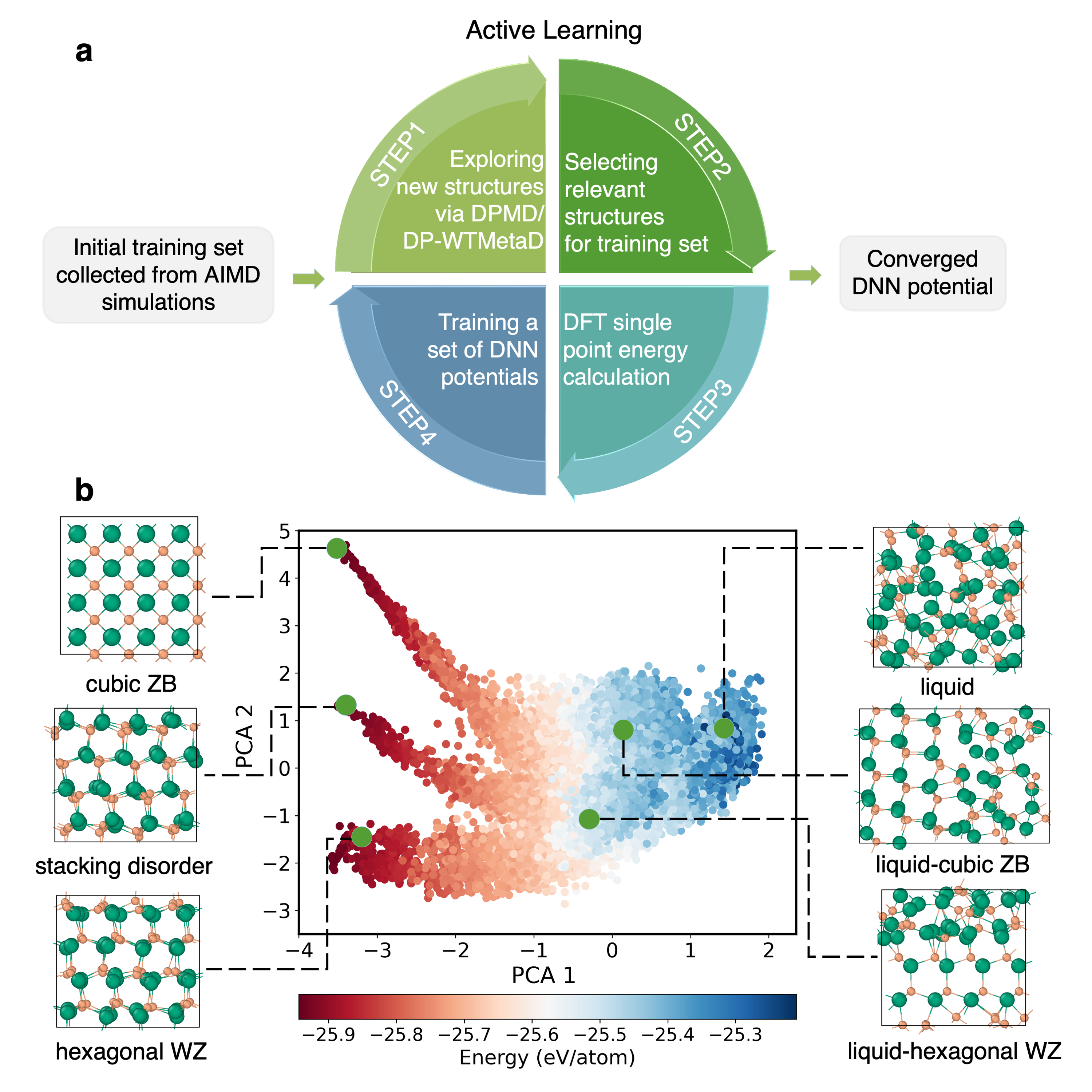
First, we built an initial training set consisting of about 4000 configurations that were collected from a few short ab initio MD (AIMD) trajectories. For AIMD calculations, two different CdSe crystals (hexagonal WZ and cubic ZB) were heated from 300 K to 2000 K into liquid.
Then, starting with these configurations and the corresponding DFT energies and atomic forces, and virials, we followed the active learning technique to extend and refine the training set. Each active learning iteration consists of the following four steps: (1) training 4 DNN potentials based on the same updated training set but with different initial training seeds; (2) exploration of the configurational space via DNN-based molecular dynamics (DPMD) simulations and their variants accelerated by WTMetaD (DP-WTMetaD). For these simulations, we performed different simulations using one of the 4 DNN potentials to sample the configurational space of different CdSe phases, such as hexagonal WZ, cubic ZB, stacking disordered, liquid, liquid-WZ, liquid-ZB, and activity transitions between these phases (see Fig. 1b). (3) selection of a small set of new relevant configurations for training set; (4) calculation of DFT energies, atomic forces, and virials for selected configurations.
For the selection of new candidate configurations in step (3), we chose the criterion of model deviation . The is defined as the maximum standard deviation of the atomic forces predicted by four DNN potentials, , where is the vector of atomic force on the atom predicted by the DNN potential , and is the average force on the atom over the four DNN potentials. We assumed that configurations with lesser than = 0.1 eV/Å have already well-represented in the training set, while those with larger than = 0.45 eV/Å are nonphysical and thus will be discarded. By this means, only structures with in the range of [ 0.1, 0.45 ] eV/Å were labeled as candidate configurations. The value of and were set up according to the suggestions given in Ref [38].
Finally, this active learning process will be exited when less than 10 candidate configurations were detected, as done in Ref [30], and a converged training set composed of about 24500 structures was obtained. The distribution of the configurational space of the training set is given in Fig. 1b. With the converged training set, we trained the final DNN potential.
All AIMD and DFT calculations were computed using the SCAN functional [39] as implemented in VASP [40, 41]. We performed all DNN-based MD simulations using the LAMMPS [42, 43] interfaced with the DeePMD-kit package, which was also used for training the DNN potentials. Enhanced sampling technique was provided by PLUMED [44]. Additional computational details can be found in Supporting Information (SI).
3 Results and Discussion
3.1 Validation of DNN potential
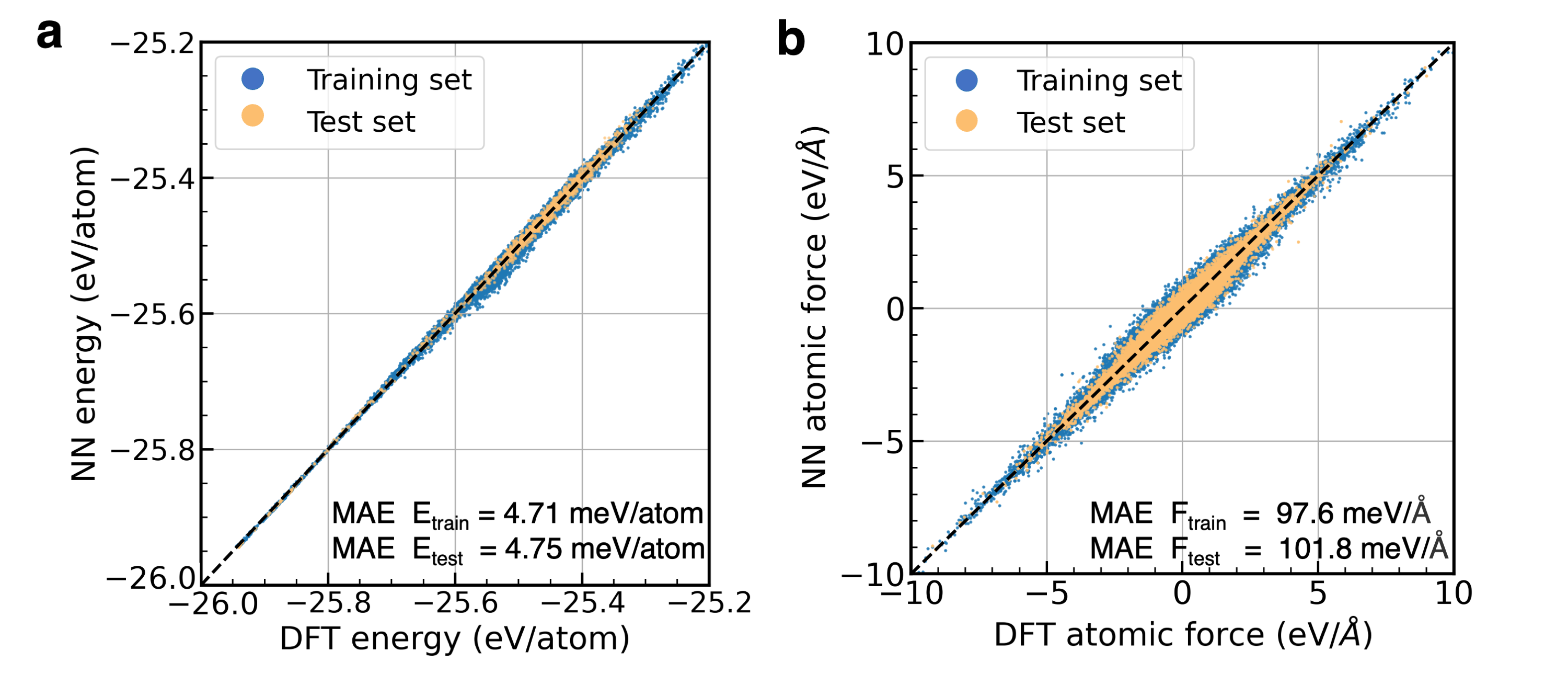
To evaluate the performance of the final DNN potential, we first checked its ability to reproduce DFT results. The comparisons of energies and atomic forces calculated on training set and test set using DFT and DNN model are given in Fig. 2. The mean absolute errors (MAEs) of energies on the training and test sets are 4.71 meV/atom and 4.75 meV/atom, respectively. The MAEs of atomic forces on training and test sets are 97.6 meV/Å and 101.8 meV/Å. The test set consists of 1500 configurations (See Fig. S5 for its configuration distribution in the 2D PCA space) collected from DPMD and DP-WTMetaD trajectories that were performed with the final DNN potential. In addition, the ground state energy of the cubic phase calculated with DNN potential is 0.6 meV/atom lower than that of the hexagonal phase, which is close to the DFT result of 0.9 meV/atom, indicating that the subtle energy difference between the cubic ZB and hexagonal WZ phases is well captured.
Furthermore, we calculated the melting temperature of CdSe crystals in hexagonal WZ and cubic ZB phases using two-phase coexisting simulations. The potential energy evolution of the simulated trajectories for melting point calculation can be seen in Fig. S6. The melting temperature of hexagonal WZ phase was estimated to be 1465.0 5.0 K, which is in good agreement with the experimental value of 1513.0 K [45]. The melting temperature of cubic ZB phase was estimated to be 1452.5 2.5 K, 12.5 K lower than that of the hexagonal WZ phase. This result coincides with the experimental findings [46] that the hexagonal WZ phase is more stable than the cubic ZB phase at high temperature.
3.2 Brute-force MD simulation of homogeneous nucleation of CdSe
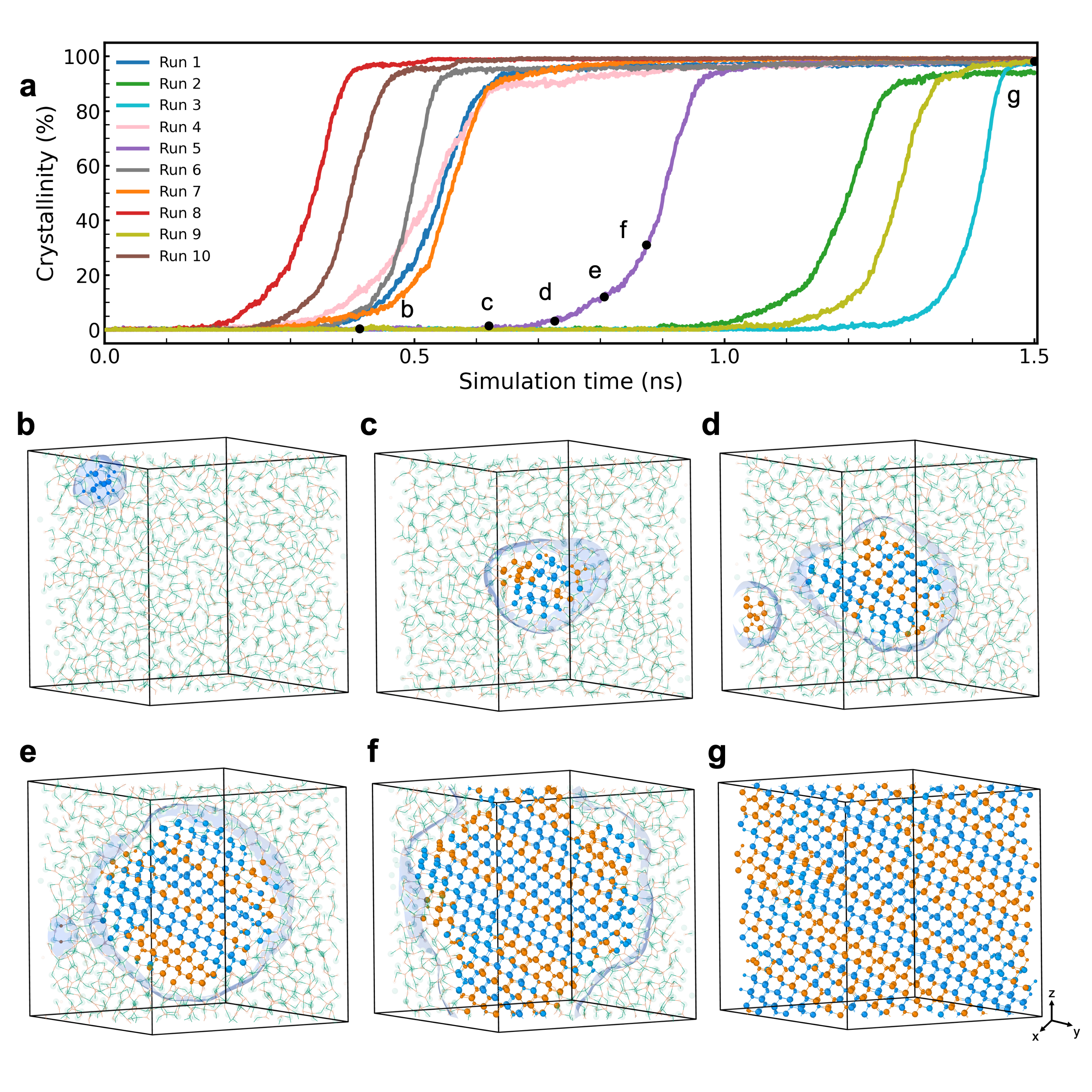
Upon cooling, liquid CdSe crystallizes into its solid phase. To investigate the evolution of the atomic structure of the nucleation process from scratch, we chose to perform brute-force MD simulations, ensuring that the intrinsic kinetics of the process were not altered. However, simulating homogeneous nucleation by MD is usually unachievable due to the large energy barrier that separates the liquid and solid phases. Thanks to the high efficiency of the DNN potential and deep supercooling condition we employed, we were able to obtain homogeneous nucleation trajectories from liquid CdSe. Fig. 3 shows the evolution of the proportion of solid-like atoms throughout ten trajectories simulated at 1000 K. After periods of apparent but divergent incubation times, ten trajectories all crystallized. The mean incubation time was estimated to be 0.54 ns. Selected representative snapshots from the trajectory of the fifth run (labeled with lowercase letters) are presented in Fig. 3b-g, showing the homogeneous nucleation process of CdSe. During the incubation period, we noticed that multiple small solid-like nuclei emerged (Fig. S7) and disappeared (Fig. 3b-c). Stochastically, one of these nuclei survives and evolves into a larger nucleus (Fig. 3c-g), eventually causing the entire liquid phase to transform into the solid phase. During the growth process of the nucleus, other small nuclei can also be formed in the remaining liquid region of the system, as demonstrated in Fig. 3d. Such nuclei can disappear or merge into the dominant nucleus.
The observation of the nucleation process shows apparently that the nucleus has a spherical-like shape, which minimizes the interfacial energy between solid and liquid phases. This phenomenon is similar to the nucleation process of silicon and ice [36, 47], suggesting that the classical nucleation theory (CNT) can approximately describe it. According to CNT, one can expect that the nucleation barrier decreases/increases as the temperature lowers/increases. To check this hypothesis, we also performed brute-force MD simulations at 900 K and 1100 K. These results indicated that multiple nuclei were formed in a relatively short time at 900 K (less than 1 ns), resulting in a polycrystalline structure (Fig. S8). In contrast, no successful nucleation event was observed at 1100 K within 25 ns. Fig. 3 shows that the nucleus is made up of hexagonal WZ and cubic ZB structure layers, resulting in a stacking disordered structure, which is consistent with previous experimental findings [48]. Interestingly, as the nucleus grows larger, the cubic ZB structure (colored blue) and hexagonal WZ structure (colored orange) can coexist in a single layer (see Fig. 3e-g). This suggests that the cubic and hexagonal structures compete with each other during the phase solidification. To gain a deeper understanding of how the stacking disordered structure is formed and the roles of Cd and Se atoms during this process, further investigations are conducted as follows.
3.3 Temperature dependence of stacking disordered structure formation
As discussed above, the relative stability and melting temperature of the cubic ZB phase differ from those of the hexagonal WZ phase, implying that the formation of the stacking disordered structure can be temperature dependent. To uncover the correlation between temperature and the formation of stacking disordered structures, we performed molecular dynamics simulations of the crystal growth of CdSe from its melt. Different thermodynamic points in the temperature range from 950 K to 1500 K (See Fig. 4) with a constant pressure of 1 bar were considered. For each temperature, we ran 25 independent simulations. These calculations were started from the same initial solid-liquid simulation cell consisting of 8640 atoms, where four hexagonal WZ layers of crystal seeds were included (Fig. 4a, see SI for more details). The growth direction was set to the z-axis of the coordinate system (along the [001] direction of the hexagonal WZ phase).
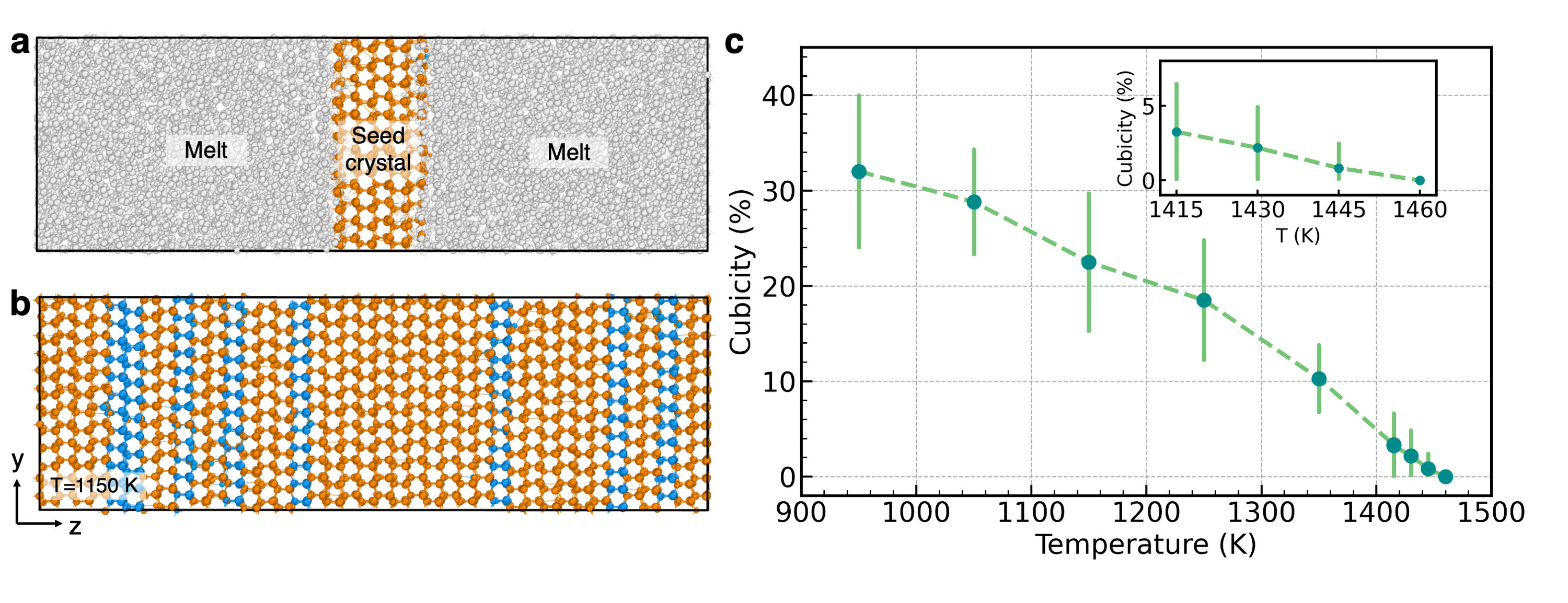
To quantify the characteristics of the stacking disordered structure obtained from growth, we calculated the cubicity, which represents the fractions of cubic ZB stacking sequences [47, 49]. Fig. 4c shows the obtained temperature dependence of the cubicity. It is clear that the lower the temperature, the higher the value of cubicity. In other words, in the lower temperature region (<1430 K), the initial solid-liquid mixed CdSe is more likely to grow into a stacking disordered structure (see Fig. 4b). Moreover, as we increase the temperature, the proportion of cubic ZB structure layers gradually decreases to zero. For instance, at 1430 K, 14 out of 25 trajectories yielded a pure hexagonal WZ phase, while the average cubicity of all 25 trajectories is only approximately 2%. Furthermore, when we increased the temperature to 1460 K, slightly lower than the melting temperature of the hexagonal phase (Tm = 1465 5 K), no stacking disordered structure was observed. These results suggest that 1430 K (corresponding to 35 K of supercooling) is approximately the lowest temperature at which we could obtain a pure hexagonal WZ phase, which is in line with the experimental Bridgman method where the low-temperature region is 50 K below the melting temperature [50]. This temperature dependence of crystallization explains why the experimental temperature to obtain the pure hexagonal WZ phase with the Bridgman method should be kept not lower than 50 K from the melting point.
3.4 Structural competition in crystallization process
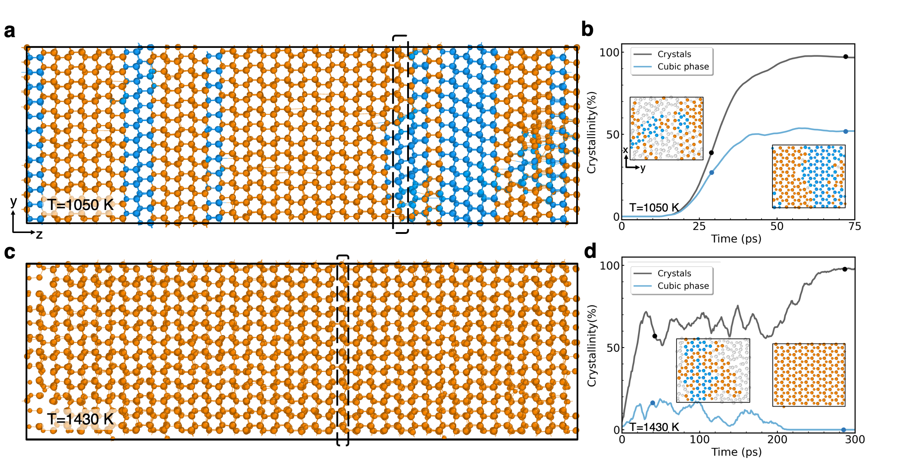
It is interesting to understand why it is easier to obtain a pure hexagonal phase when we increase the temperature of crystal growth. Actually, during the crystal growth process, various defects appeared and persisted, and their performances were closely related to temperature. Two crystal snapshots (with a projection of the y-z plane) taken from typical crystallization simulations at 1050 K and 1430 K are illustrated in Fig. 5a and c, respectively. For each case, we followed the crystal formation of two atomic layers highlighted by the black box, as shown in Fig. 5b and d (with a projection of the x-y plane). It is obvious that in both situations, stacking competition between cubic ZB and hexagonal WZ in the same layer occurred during crystal growth. As the crystal grows, for the case of 1050 K, cubic ZB atoms are frozen without further rearrangement, resulting in a manner of two-phase coexistence (Fig. 5a). In contrast, for the case of 1430 K, cubic ZB atoms are more likely to be converted into the hexagonal WZ phase after a period of structural fluctuation and rearrangement, and the proportion of cubic ZB atoms fluctuates and approaches zero as time evolves, leading to a pure phase of hexagonal WZ (Fig. 5c).
3.5 Microscopic mechanism of CdSe crystallization
The structure of solid CdSe consists of an equal number of tetracoordinated Cd and Se atoms placed at alternate tetrahedral points of a diamond lattice, as depicted in Fig. 6a. A straightforward hypothesis of its crystallization process would be that each type of atom is attached to the solid-liquid interface one by one so that an alternating arrangement of Cd and Se atoms can be formed. Nevertheless, a careful examination of the the evolution process of the interfacial region during the growth process reveals a completely different narrative, where the behaviors of Cd and Se atoms exhibits significant disparties.
The detailed crystallization mechanism of CdSe was studied using one of the representative trajectories of the CdSe crystal growth at 1415 K. Specifically, we followed the formation processes of four new crystallized layers denoted by capital letters A, B, C, and D in Fig. 6f, respectively. To quantify the dynamical behaviour of each type of atom from different layers, we calculated the mean square displacements (MSDs) for Cd and Se atoms in each layer as a function of time. The MSD value for atoms in each layer at time t was calculated as follows and the instantaneous structure at time ps when the studied four atomic layers crystallized was set as a reference point.
| (1) |
in which N means the number of Cd or Se atoms in each layer and ri(t) is the position of the ith atom at time t.
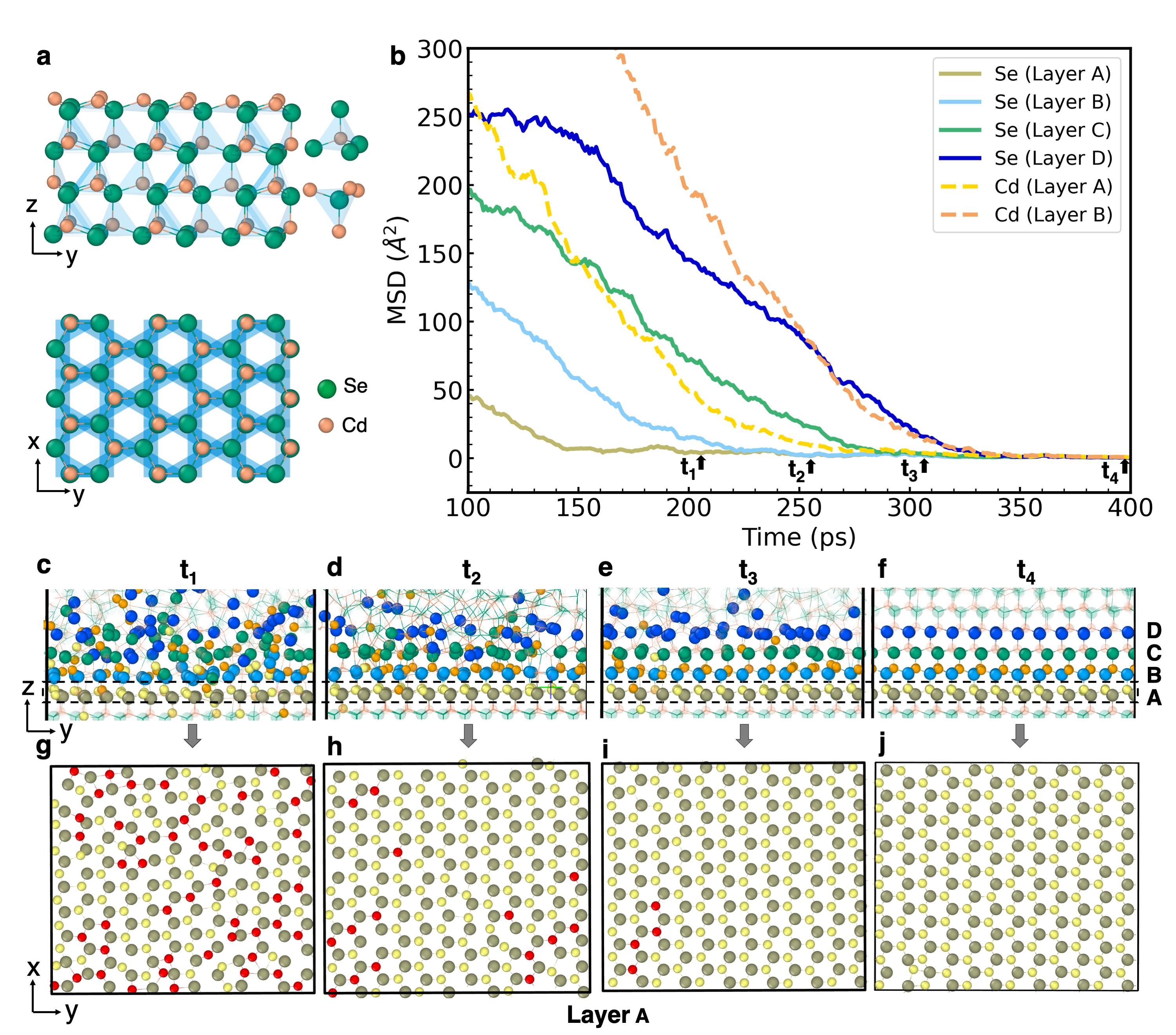
The obtained MSDs for Cd and Se atoms in different layers as a function of time are presented in Fig. 6b. The smaller the MSD value, the higher the crystallinity of the atomic layer. Once all Cd or Se atoms in a given layer were crystallized, the corresponding MSD curves approach zero. Counterintuitively, we find that the MSDs of Cd and Se atoms for the same layer do not reach zero simultaneously, rather an approximately 100 ps delay is noticed in the MSD curve of Cd compared with that of Se as shown in Fig. 6b, indicating a rather complex mechanism underlying the crystallization process of CdSe.
For instance, at t1 (see Fig. 6c and Fig. 6g), Se atoms in layer A were well arranged in their lattice with an MSD value close to zero (dark-khaki line in Fig. 6b), while the Cd atoms in the same layer still have a relatively large MSD value of 45 Å2 (yellow dotted line in Fig. 6b).
Furthermore, we find that the crystallization of Cd atoms is not only affected by its short-range atomic environment but also strongly connected with the medium-range ordering of Se and Cd atoms. As illustrated in Fig. 6d at , all lattice points of Se atoms in both layers A and B were filled, resulting in tetrahedrons that favor the occupation of the Cd atoms in their center.
The cross-section snapshot of layer A (Fig. 6h) confirmed this argument that all tetrahedron centers of Se clusters were placed with Cd atoms. However, some of these Cd atoms (red marked atoms in Fig. 6h) were not yet stable and would migrate to other places as the crystal grew. With further analysis, we found that the crystallization of Se atoms in layer C was essential to stabilize the Cd atoms in layer A. Once the lattice sites of Se atoms in layer C were arranged, similarly, tetrahedral sites consisting of Se atoms from layer B and C were formed in favor of the occupation of the Cd atoms in layer B. Importantly, this arrangement stabilized the Cd atoms in layer A by forming perfect tetrahedrons consisting of Cd atoms from layers A and B. In addition, the MSDs of Cd atoms in layer A and Se atoms in layer C reach zero approximately concertedly at t3.
A similar phenomenon was also observed in layer B, in which Cd atoms in this layer were stabilized until Se atoms in layer D found their positions. Therefore, the cooperative actions between Cd and Se atoms within the medium range region dominate the crystallization process of CdSe.
We suggest that this quite different behavior of Se and Cd atoms during the crystallization process is closely related to the radii of Se2- and Cd2+ ions. The ionic radius of Se2- is 1.84 Å, while that of Cd2+ is only 0.92 Å [51]. This large difference in ion radii makes Cd atoms more mobile than Se atoms. To confirm this argument, the diffusion coefficients for Se2- () and Cd2+() at temperatures from 1100 K to 1500 K for liquid CdSe (See SI for more details) were calculated. We found that the calculated were at least two times larger than .
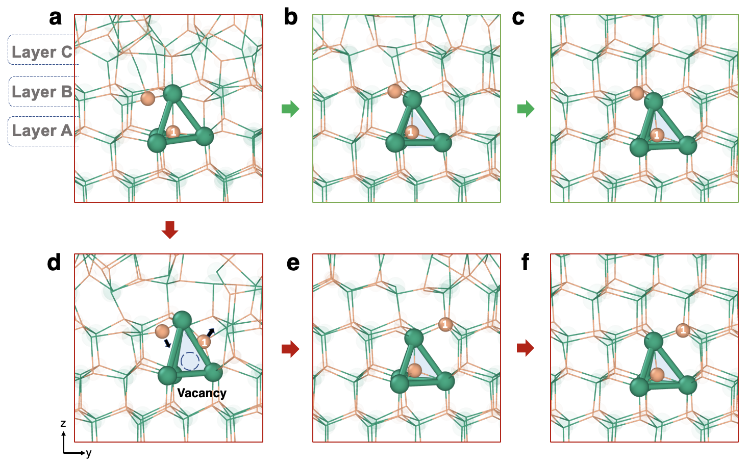
To gain a closer mechanism of the crystallization of Cd atoms, we analysed the movement of Cd atoms in layer A located in the tetrahedral center of Se, corresponding to those discussed in Fig. 6h at time . Two possible pathways as illustrated in Fig. 7 were located. Cd atoms can either stay at the tetrahedron center of Se (pathway: a b c) or migrated to other layers (pathway: a d e f). At the starting point, Se atoms in layers A and B were well arranged at their lattice sites forming a perfect tetrahedron (green ball-and-stick marked in Fig. 7a), while those in layer C were randomly distributed. Stabilization by the tetrahedron of Se, Cd atoms preferred to be located at the center of the tetrahedron resulting in a pathway of a b c. However, without the stabilization from Se atoms in layer C, Cd atoms in layer B are super mobile, which pushes the Cd1 atom in layer A to move away from the original site and leave a vacancy (Fig. 7d). Subsequently, Cd atoms in layer B moved to this vacancy and occupied the original position of Cd1 (Fig. 7d-e), leading to another pathway of a d e f. Taken together, we can see that Cd atoms in layer A were not stabilized until their third-shell neighbor atoms Se find their position. Therefore, the medium-range ordering of Se atoms governs the nucleation and growth process of CdSe.
4 Conclusion
In this work, we have developed a DNN potential with ab initio accuracy using an enhanced sampling-accelerated active learning approach to investigate the crystallization process of CdSe. With this potential, we conducted molecular dynamics simulations for systems containing 8640 atoms, enabling us to systematically study the crystallization mechanism of CdSe at atomic level. Brute-force simulations were first performed to study the nucleation process of CdSe. We found that a spherical-like nucleus was formed, consistent with classical nucleation theory. To elucidate the growth mechanism, we then performed MD simulations of CdSe growth from its melt at temperatures ranging from 950 K to 1500 K. Our results demonstrated that the formation of stacking disordered structures was temperature-dependent, and a pure hexagonal WZ crystal can only be obtained above 1430 K, 35 K below its melting temperature, in line with the experimental observations using the Bridgman method. By analysing the crystallization process in detail, we found that the dynamic behaviors and solidification paces of Cd and Se atoms were markedly different, primarily due to the difference between the ionic radius of Se2- and Cd2+. Specifically, lower mobility Se atoms pioneered the solidification process by forming tetrahedrons, followed by Cd atoms occupying centers of these tetrahedrons and settling down until the third-shell neighbor of Se atoms found their lattice positions. In other words, the medium-range ordering of Se atoms governs the crystallization process of CdSe. Consequently, the underlying crystallization mechanism of CdSe, shaped by the distinct dynamical behavior of Cd and Se atoms, is much more intricate than anticipated. Our findings highlight the crucial role of the complex dynamical process that governs the quantity of synthesized crystals. Molecular dynamics simulation aided by quality machine learning potential is a powerful tool for studying such processes.
CRediT authorship contribution statement
Linshuang Zhang: Performed calculations, Analyzed the data, Wrote the paper. Manyi Yang: Conceptualization, Methodology, Performed calculations, Analyzed the data, Wrote the paper. Shiwei Zhang: Performed enhanced sampling simulations, Analyzed the data. Haiyang Niu: Conceptualization, Methodology, Analyzed the data, Wrote the paper, Funding acquisition, Supervision.
Declaration of competing interest
The authors declare that they have no known competing financial interests or personal relationships that could have appeared to influence the work reported in this paper.
Acknowledgment
The authors would like to thank Mingfeng Liu, Jingwei Zhang, Junwei Hu and Mingyi Chen for their valuable contributions to the discussions. This work was supported by the National Natural Science Foundation of China (grant No. 22003050), the National Science Fund for Excellent Young Scientist Fund Program (Overseas) of China, the Science and Technology Activities Fund for Overseas Researchers of Shaanxi Province, China, and the Research Fund of the State Key Laboratory of Solidification Proceeding (NWPU) of China (No. 2022-QZ-03). The calculations were supported by the International Center for Materials Discovery (ICMD) cluster of NWPU and the Swiss National Supercomputing Centre (CSCS) under project ID and .
References
- [1] S. Ninomiya, S. Adachi, Optical properties of cubic and hexagonal CdSe, J. Appl. Phys. 78 (7) (1995) 4681–4689.
- [2] S. H. Park, M. P. Casey, J. Falk, Nonlinear optical properties of CdSe quantum dots, J. Appl. Phys. 73 (12) (1993) 8041–8045.
- [3] J. H. Yuan, X. M. Duan, B. Q. Yao, Z. Cui, Y. Y. Li, T. Y. Dai, Y. J. Shen, Y. L. Ju, Tunable 10- to 11- µm CdSe optical parametric oscillator pumped by a 2.1-µm Ho:YAG laser, Appl. Phys. B 122 (7) (2016) 202.
- [4] J. Yuan, Y. Chen, X. Duan, B. Yao, T. Dai, Y. Ju, CdSe optical parametric oscillator operating at 12.07 µm with 170 mW Output, Opt. Laser Technol. 92 (2017) 1–4.
- [5] N. C. Greenham, X. Peng, A. P. Alivisatos, Charge separation and transport in conjugated-polymer/semiconductor-nanocrystal composites studied by photoluminescence quenching and photoconductivity, Phys. Rev. B 54 (1996) 17628–17637.
- [6] M. Schierhorn, S. W. Boettcher, S. Kraemer, G. D. Stucky, M. Moskovits, Photoelectrochemical performance of CdSe nanorod arrays grown on a transparent conducting substrate, Nano Lett. 9 (9) (2009) 3262–3267.
- [7] M. C. Schlamp, X. Peng, A. P. Alivisatos, Improved efficiencies in light emitting diodes made with CdSe(CdS) core/shell type nanocrystals and a semiconducting polymer, J. Appl. Phys. 82 (11) (1997) 5837–5842.
- [8] H. Mattoussi, L. H. Radzilowski, B. O. Dabbousi, E. L. Thomas, M. G. Bawendi, M. F. Rubner, Electroluminescence from heterostructures of poly(phenylene vinylene) and inorganic CdSe nanocrystals, J. Appl. Phys. 83 (12) (1998) 7965–7974.
- [9] M. Bruchez, M. Moronne, P. Gin, S. Weiss, A. P. Alivisatos, Semiconductor nanocrystals as fluorescent biological labels, Science 281 (5385) (1998) 2013–2016.
- [10] W. C. W. Chan, S. Nie, Quantum dot bioconjugates for ultrasensitive nonisotopic detection, Science 281 (5385) (1998) 2016–2018.
- [11] J. Steininger, Growth of CdSe single crystals by temperature gradient solution zoning in excess Se, Mat. Res. Bull. 3 (7) (1968) 595–598.
- [12] Y. Ni, H. Wu, M. Mao, W. Li, Z. Wang, J. Ma, S. Chen, C. Huang, Growth and characterization of mid-far infrared optical material CdSe crystal, Opt. Mater. Express 8 (7) (2018) 1796–1805.
- [13] N. N. Kolesnikov, R. B. James, N. S. Berzigiarova, M. P. Kulakov, HPVB and HPVZM shaped growth of CdZnTe, CdSe, and ZnSe crystals, Proc. SPIE 4784 (2002) 93–104.
- [14] S. M. Hughes, A. P. Alivisatos, Anisotropic formation and distribution of stacking faults in II–VI semiconductor nanorods, Nano Letters 13 (1) (2013) 106–110.
- [15] L. Qu, Z. A. Peng, X. Peng, Alternative routes toward high quality CdSe nanocrystals, Nano Letters 1 (6) (2001) 333–337.
- [16] C. Y. Yeh, Z. W. Lu, S. Froyen, A. Zunger, Zinc-blende–wurtzite polytypism in semiconductors, Phys. Rev. B 46 (1992) 10086–10097.
- [17] J. Huang, M. V. Kovalenko, D. V. Talapin, Alkyl chains of surface ligands affect polytypism of CdSe nanocrystals and play an important role in the synthesis of anisotropic nanoheterostructures, J. Am. Chem. Soc 132 (45) (2010) 15866–15868.
- [18] P. Villars, S. Iwata, PAULING file verifies/reveals 12 principles in materials science supporting four cornerstones given by nature, Chem. Met. Alloy. 6 (2013) 81–108.
- [19] L. Bonati, M. Parrinello, Silicon liquid structure and crystal nucleation from ab initio deep metadynamics, Phys. Rev. Lett 121 (2018) 265701.
- [20] H. Niu, P. M. Piaggi, M. Invernizzi, M. Parrinello, Molecular dynamics simulations of liquid silica crystallization, Proc. Natl Acad. Sci. 115 (21) (2018) 5348–5352.
- [21] H. Niu, Y. I. Yang, M. Parrinello, Temperature dependence of homogeneous nucleation in ice, Phys. Rev. Lett 122 (24) (2019) 245501.
- [22] M. Chen, L. Tan, H. Wang, L. Zhang, H. Niu, Imperfectly coordinated water molecules pave the way for homogeneous ice nucleation, arXiv:2304.12665 (Apr. 2023).
- [23] L. Guo, S. Zhang, W. Feng, G. Hu, W. Li, A first-principles study on the structural, elastic, electronic, optical, lattice dynamical, and thermodynamic properties of zinc-blende CdX (X=S, Se, and Te), J. Alloys Compd 579 (2013) 583–593.
- [24] S. Chanda, M. Debbarma, D. Ghosh, S. Das, B. Debnath, R. Bhattacharjee, S. Chattopadhyaya, Cationic and anionic concentration dependent elastic properties of zinc blende specimens within CdxZn1-xSySe1-y quaternary system: Calculations with density functional theory, Solid State Commun. 322 (2020) 114050.
- [25] Z. Deng, L. Cao, F. Tang, B. Zou, A new route to zinc-blende CdSe nanocrystals: Mechanism and synthesis, J. Phys. Chem.B 109 (35) (2005) 16671–16675.
- [26] J. Behler, M. Parrinello, Generalized neural-network representation of high-dimensional potential-energy surfaces, Phys. Rev. Lett 98 (2007) 146401.
- [27] J. Behler, Perspective: Machine learning potentials for atomistic simulations, J. Chem. Phys 145 (17) (2016) 170901.
- [28] H. Wang, L. Zhang, J. Han, W. E, DeePMD-kit: A deep learning package for many-body potential energy representation and molecular dynamics, Comput. Phys. Commun. 228 (2018) 178–184.
- [29] H. Niu, L. Bonati, P. M. Piaggi, M. Parrinello, Ab initio phase diagram and nucleation of gallium, Nat. Commun. 11 (1) (2020) 2654.
- [30] M. Yang, T. Karmakar, M. Parrinello, Liquid-liquid critical point in phosphorus, Phys. Rev. Lett 127 (2021) 080603.
- [31] M. Yang, L. Bonati, D. Polino, M. Parrinello, Using metadynamics to build neural network potentials for reactive events: the case of urea decomposition in water, Catal. Today 387 (2022) 143–149.
- [32] L. Zhang, H. Wang, R. Car, W. E, Phase diagram of a deep potential water model, Phys. Rev. Lett 126 (2021) 236001.
- [33] M. Galib, D. T. Limmer, Reactive uptake of N2O5 by atmospheric aerosol is dominated by interfacial processes, Science 371 (6532) (2021) 921–925.
- [34] A. Laio, M. Parrinello, Escaping free-energy minima, Proceedings of the National Academy of Sciences 99 (20) (2002) 12562–12566.
- [35] L. Zhang, J. Han, H. Wang, R. Car, W. E, Deep potential molecular dynamics: A scalable model with the accuracy of quantum mechanics, Phys. Rev. Lett 120 (2018) 143001.
- [36] L. Bonati, M. Parrinello, Silicon liquid structure and crystal nucleation from ab initio deep metadynamics, Phys. Rev. Lett 121 (26) (2018) 265701.
- [37] J. Deng, H. Niu, J. Hu, M. Chen, L. Stixrude, Melting of MgSiO3 determined by machine learning potentials, Phys. Rev. B 107 (2023) 064103.
- [38] Y. Zhang, H. Wang, W. Chen, J. Zeng, L. Zhang, H. Wang, W. E, DP-GEN: A concurrent learning platform for the generation of reliable deep learning based potential energy models, Comput. Phys. Commun. 253 (2020) 107206.
- [39] J. Sun, A. Ruzsinszky, J. P. Perdew, Strongly constrained and appropriately normed semilocal density functional, Phys. Rev. Lett 115 (2015) 036402.
- [40] G. Kresse, J. Hafner, Ab initio molecular dynamics for liquid metals, Phys. Rev. B 47 (1993) 558–561.
- [41] G. Kresse, J. Furthmüller, Efficient iterative schemes for ab initio total-energy calculations using a plane-wave basis set, Phys. Rev. B 54 (1996) 11169–11186.
- [42] S. Plimpton, Fast parallel algorithms for short- range molecular dynamics, J. Comput. Phys. 117 (1) (1995) 1–19.
- [43] A. P. Thompson, H. M. Aktulga, R. Berger, D. S. Bolintineanu, W. M. Brown, P. S. Crozier, P. J. in ’t Veld, A. Kohlmeyer, S. G. Moore, T. D. Nguyen, R. Shan, M. J. Stevens, J. Tranchida, C. Trott, S. J. Plimpton, Lammps - a flexible simulation tool for particle-based materials modeling at the atomic, meso, and continuum scales, Comput. Phys. Commun. 271 (2022) 108171.
- [44] G. A. Tribello, M. Bonomi, D. Branduardi, C. Camilloni, G. Bussi, PLUMED 2: New feathers for an old bird, Comput. Phys. Commun. 185 (2) (2014) 604–613.
- [45] D. R. Lide, CRC handbook of chemistry and physics, CRC Press (2005).
- [46] V. Fedorov, V. Ganshin, Y. N. Korkishko, Determination of the point of the zincblende-to-wurtzite structural phase transition in cadmium selenide crystals, Phys. Status Solidi 126 (1) (1991) K5–K7.
- [47] H. Niu, Y. I. Yang, M. Parrinello, Temperature dependence of homogeneous nucleation in ice, Phys. Rev. Lett 122 (2019) 245501.
- [48] A. Yoshiasa, K. Koto, H. Maeda, T. Ishii, The mean-square relative displacement and displacement correlation functions in tetrahedrally and octahedrally coordinated ANB8-N crystals, Jap. J. Appl. Phys. 36 (1997) 781.
- [49] L. Lupi, A. Hudait, B. Peters, M. Grünwald, R. G. Mullen, A. H. Nguyen, V. Molinero, Role of stacking disorder in ice nucleation, Nature 551 (7679) (2017) 218.
- [50] Y. Ni, H. Wu, M. Mao, W. Li, Z. Wang, J. Ma, S. Chen, C. Huang, Growth and characterization of mid-far infrared optical material CdSe crystal, Opt. Mater. Express 8 (7) (2018) 1796–1805.
- [51] O. Parasyuk, L. Gulay, L. Piskach, I. Olekseyuk, The Ag2Se–CdSe–SnSe2 system at 670 K and the crystal structure of the Ag2CdSnSe4 compound, J. Alloys Compd 335 (1) (2002) 176–180.