Data acquisition system for muon tracking in a muon scattering tomography setup
Abstract
We report here the development of a multi-channel DAQ system for muon tracking in a muon scattering tomography setup. The salient features of the proposed DAQ system are direct acquisition and processing of LVDS signals, 500MHz sampling frequency and scalability. It consists of front-end electronics stage built around NINO ASIC. The back-end electronics is configured with Intel®/Altera® MAX®-10 FPGA development board which transmits data to the storage following UART protocol. The proposed DAQ system has been tested for its performance using a position sensitive glass RPC detector with two-dimensional 8 8 readout strip configuration.
keywords:
Muon Scattering Tomography , NINO ASIC , Field Programmable Gate Array , FPGA-based DAQ ,[inst1]organization=Saha Institute of Nuclear Physics, A CI of Homi Bhabha National Institute, addressline=Sector I, AF Block, Bidhannagar, city=Kolkata, postcode=700064, country=India
[inst2]organization=University of California, addressline=One Shields Ave, Davis, city=California, postcode=95616, country=USA
[inst3]organization=Center for Frontiers in Nuclear Science, Department of Physics and Astronomy, addressline=Stony Brook University, 100 Nicolls Road, Stony Brook, city=New York, postcode=11794, country=USA
1 Introduction
Muon Scattering Tomography (MST) is a non-destructive evaluation technique used for investigating the internal structure and constituent materials of a large and static object by utilizing the principle of multiple Coulomb scattering of cosmic ray muons. While passing through matter medium, the muons can suffer scattering owing to their electromagnetic interaction with the atomic nuclei present in the medium [1, 2, 3, 4, 5, 6]. The net deflection of a muon from its original trajectory can be represented as a Gaussian distribution with standard deviation dependent on the momentum of muon and thickness of the object in terms of radiation length vis-a-vis its atomic number and density [7, 8, 9]. Therefore, determination of scattering angle by tracking the muon trajectory can be utilized to identify the material if the muon momentum is known. The tracking of muon may be accomplished with a series of position sensitive detectors placed along the direction of muon propagation. The two-dimensional position information of the muon event obtained from each of them can be used to reconstruct the trajectory of the muon. The scattering angle eventually can be determined from the incident and scattered trajectories reconstructed using positions of the muon events at the tracking detectors placed respectively before and after their passage through the object.
Gaseous detectors are frequently used as tracking devices for their excellent position and timing resolutions. A few more advantages, like low cost and relatively easy production of large area coverage add to their wide acceptance in this area of application [10, 11]. To ensure precise measurement of scattering angle, which can be as small as few mrad for low density materials, like Aluminium, the position resolution of the detectors should be of the order of few hundreds of [6, 12]. Obviously, fairly high readout granularity with finer strip width of the order of mm or less is an essential requisite for this to achieve. Eventually, the higher granularity combined with sufficiently large coverage of the tracking detectors calls for a large number of readout channels. Therefore, a cost effective solution for the readout electronics turns out extremely important in planning and designing of such an application. For data acquisition of a setup with large number of input channels, FPGA based systems offer the optimal solution for the backend signal processing and control because of the availability of large number of I/O, parallel operation, software controlled reconfigurability and cost effectiveness.
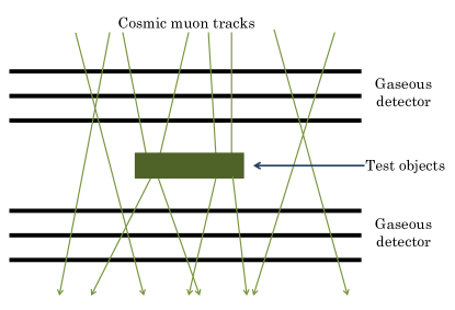
We have aimed to build a prototype setup for material discrimination utilizing the technique of MST with an objective of its application in inspection of civil structures [13, 14]. In the initial phase, we plan to implement single-gap Resistive Plate Chamber (RPC) as position sensitive tracking detector in the setup for detection of muon. The RPC in particular has been opted for its simple and robust design, easy construction using inexpensive materials, yet, very efficient performance along with excellent position and timing resolution. The design and choice of materials for fabricating the RPC have been optimized with numerical simulation of the electrical properties of the detector [15]. In the setup, two sets of RPC, each containing three of them, will be commissioned above and below the inspection volume. The two-dimensional position information of the muon events recorded by the RPCs in each set will be used to reconstruct the trajectories and determine the scattering angle subsequently. A schematic layout of the prototype MST setup has been shown in figure 1. The design has been optimized with detailed numerical modelling and simulation of its performance [6]. In future, the RPCs may be replaced with new generation Micro-Patterrn Gaseous Detectors (MPGDs) to achieve more precise position information and improved performance of the MST setup.
We have configured a multi-parameter Data AcQuisition (DAQ) system for acquiring two-dimensional position information (X,Y) of muon events from the RPCs and their storage for further processing. It comprises of a front-end stage receiving the analog signals from the RPCs followed by a back-end stage for acquisition of valid information and their transmission to a permanent storage for subsequent data analysis. The scheme and a few preliminary test results of the DAQ system have been reported by us in an earlier publication [16]. In the current paper, we present a detailed report on its configuration along with performance test done using a single-gap glass RPC prototype.
In the following section 2, a comprehensive description of the DAQ configuration with front-end and back-end electronics has been furnished along with their functionality. The performance of the DAQ system has been validated with several measurements which can be found in section 3 along with the results. Finally, the section 4 has presented the summary and conclusion of the work.
2 DAQ Configuration
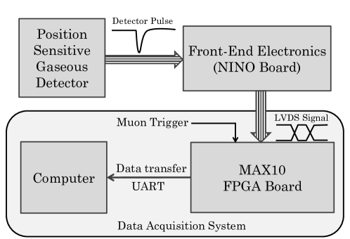
The direct acquisition from the readout channels of the RPC has been done by Front-End Electronics (FEE), built around a low-power, ultra-fast, amplifier discriminator ASIC, namely NINO, fabricated with 0.25 m CMOS technology. It was initially developed for the Multi-gap Resistive Plate Chambers (MRPCs) in the Time-of-Flight (TOF) array of the ALICE experiment [17, 18]. The Low Voltage Differential Signal (LVDS) output from the FEE has been transferred to the Back-End Electronics (BEE), configured with Altera/Intel® MAX®-10 FPGA. It is a low-cost, single chip with small form factor and programmable logic device. As and when prompted by trigger, the BEE has acquired and saved the valid LVDS signals in parallel and transmitted the data in serial manner to a personal computer (PC) following Universal Asynchronous Receiver / Transmitter (UART) protocol for permanent storage. The schematic diagram of the proposed DAQ system has been illustrated in figure 2. The design and configuration of FEE and BEE stages have been described in the following sections 2.1 and 2.2, respectively.
2.1 Front-End Electronics (FEE)
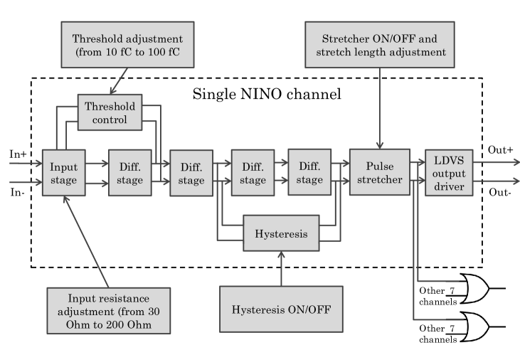
The NINO ASIC has been built as a discrminator to produce an output by measuring Time-Over-Threshold (TOT) of the input signal for slewing correction. The TOT is actually a measure of time lapsed between the leading and trailing edges of the input pulse when they surpass a specific threshold level of charge. The ASIC has been designed on the basis of a current to voltage converter with a common gate circuit configuration followed by four cascaded amplifiers with low gain and high bandwidth. There is a slow feedback circuit to supply current for keeping the input stages correctly biased. An offset is added here to adjust the threshold level for the measurement of TOT. Finally, a stretcher is used before the LVDS output driver in order to match the width requirement foreseen for any readout system. The NINO takes differential input and its circuit is differential throughout to achieve an improved immunity to cross talk. The architecture of one of its readout channels has been schematically presented in figure LABEL:fig:nino_channel. The characteristic features of the NINO have been furnished below.
-
1.
8 input channels of either polarity
-
2.
Adjustable threshold level of 10–100fC
-
3.
Fast amplification with peaking time 1ns and rms resolution 20ps
-
4.
8 LVDS output channels with level difference 300mV and time jitter 25ps
-
5.
Operate with input capacitance 30pF
-
6.
Power consumption 40mW per channel
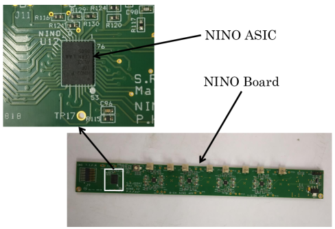
A readout board of dimension 200mm 23mm, with a common threshold control for all the channels has been designed with a single NINO by the TIFR and INO Collaboration [19], as shown in figure LABEL:fig:nino_board. The board accepts either of the positive and negative polarity signals which is converted into the differential type and fed to the inputs of the NINO. The voltage requirement for the operation of the said board is 4V. We have utilised the same NINO-board as the FEE of the present DAQ system.
2.2 Back-End Electronics (BEE)
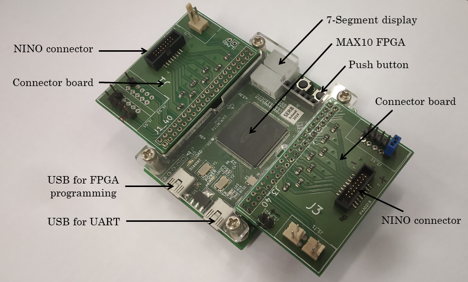
The BEE stage has been configured using Altera®/Intel® MAX®-10 FPGA-based development board. One of the salient features of the said board is that it has dedicated I/O for direct acquisition of LVDS signals produced by the FEE. This eliminates the necessity of conversion of LVDS signals to TTL type before the BEE stage and thereby, LVDS signal purity is maintained. To map the LVDS connections between the FEE and BEE boards, a custom-designed connector board has been fabricated, as shown in figure 4, with required 100 termination. The important features of the said FPGA-board have been mentioned below.
-
1.
2000 Logic Elements (LEs)
-
2.
108 embedded memory blocks (Kbits)
-
3.
12 user flash memory (KBytes)
-
4.
Single internal configuration memory
-
5.
16 embedded 18 x 18 multipliers
-
6.
Phase Lock Loop (PLL) with maximum clock frequency 500MHz
-
7.
101 I/O pins
-
8.
On-board clock frequency 50MHz
-
9.
CH340G chip-based USB-UART converter
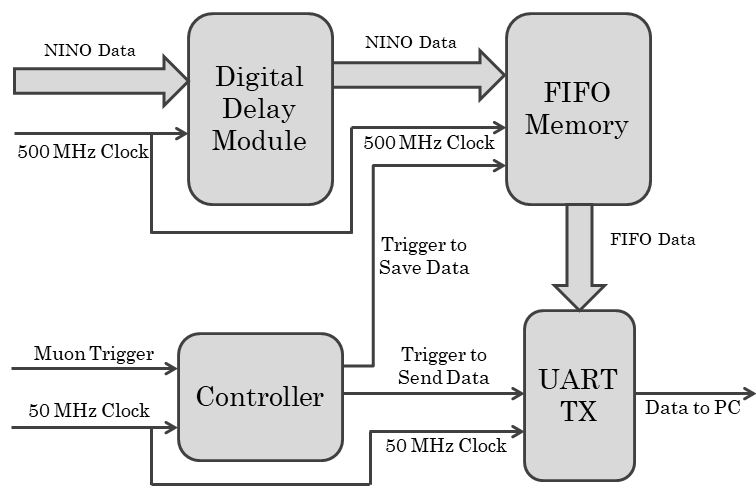
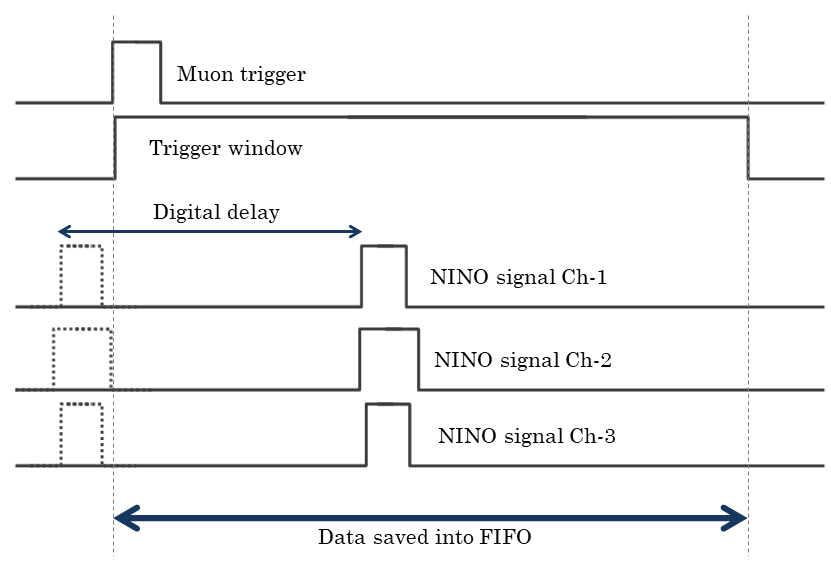
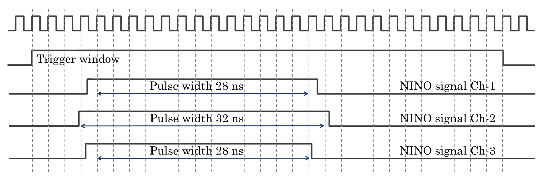
The code for signal acquisition and data transfer by the MAX®-10 FPGA has been developed on the VHSIC Hardware Description Language (VHDL) platform. A custom IP (Intellectual Property) core consisting of four components, namely, digital delay module, controller, FIFO memory and UART module with TX pin, has been generated for this purpose. The flowchart of the IP core has been depicted in figure LABEL:fig:FPGA_operation_a. The Intel® Quartus® Prime software has been used to compile and upload the configuration code. It has been implemented in each of the input channels. The on-board Phase Lock Loop (PLL) facilitates generation of variable clock frequencies up to a maximum of 500MHz for sampling. A clock frequency 500MHz, as generated by the PLL, has been used for sampling data in the delay module and FIFO memory to achieve 2ns resolution while the frequency 50MHz generated by the on-board clock has been used for the controller and UART TX module. When prompted by a trigger, the controller has produced 260ns wide window. A digital delay of 128ns has been added to the LVDS signal received from NINO to ensure its position inside the trigger window, as shown in figure LABEL:fig:FPGA_operation_b. The FIFO memory has been used to store the entire data lying inside the trigger window. When prompted by the controller module, the data have been transmitted to the connected PC through the TX pin of the UART. The information acquired for each channel for each trigger have been saved in the PC for further offline analysis. A code based on Python programming language has been developed and used to acquire data on the PC using COM port and analyse subsequently.
3 DAQ Performance
The proposed DAQ system has been tested for its performance to acquire the signals produced by cosmic muons in a single-gap glass RPC prototype. The experimental setup has been described in the next section 3.1. It has been followed by the section 3.2 where the functioning of the DAQ system for acquisition of RPC signal has been discussed along with the measurement of efficiency of the detector for muon detection. In the next section 3.3, the process of trigger validation using different physical setups and logic conditions have been presented along with the results. The scalability of the DAQ system has been tested by studying the muon event distribution detected by the whole RPC prototype using different configuration of the DAQ system. This has been discussed in section 3.4.
3.1 Experimental Setup
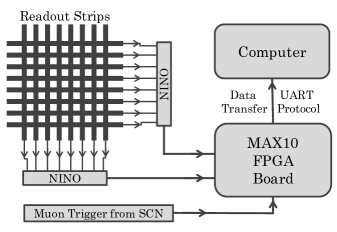
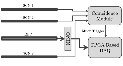
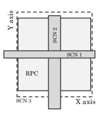
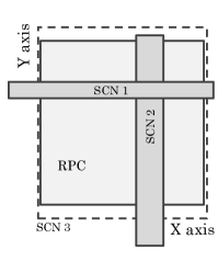
A prototype RPC made with 2mm 30cm 30cm float glass plates as resistive electrodes and 2mm gas gap has been used for detecting cosmic muons. A gas mixture of 95% Freon and 5% Isobutane has been circulated through the detector. Two readout panels each consisting of eight copper strips of width 3cm and separation 2mm have been used for recording two-dimensional (X,Y) position information. The panels have been placed in orthogonal manner to each other outside the glass electrodes and insulated by a layer of mylar. The readout scheme of the RPC prototype has been illustrated in figure LABEL:fig:detector_config_xy. It shows that two NINO-boards of the FEE stage have been connected to two readout panels for receiving detector analog signals produced by the passage of muons. The LVDS signals generated by the pair of NINO-boards corresponding to the RPC signal have been transmitted to an Altera®/Intel® MAX®-10 FPGA-board of the BEE stage via the custom designed connector board. The signals have been stored in the BEE when prompted by the muon trigger produced from the coincidence of the scintillators and the data subsequently have been transmitted to the PC. Several plastic scintillators of different dimensions have been used in the setup for testing the DAQ system with different trigger conditions. The schematic of the experimental setup for testing the RPC prototype using three scintillators (SCN1, SCN2, SCN3) as trigger detectors has been illustrated in figure LABEL:fig:detector_config_z. The SCN1 and SCN2 are two finger-shaped scintillators with length 35cm and their widths are 3cm and 5cm, respectively. The third scintillator has an area 25cm 35cm which has an overlap with the entire active area of the RPC.
3.2 Detector Signal Acquistion
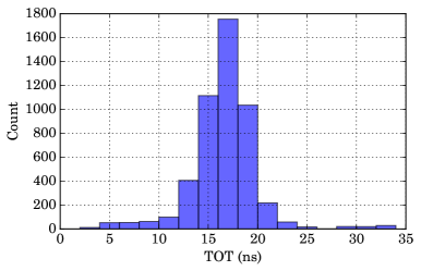
Upon passage of a cosmic muon through the active gaseous medium of the RPC, an avalanche of electron-ion pairs is produced from ionization of gaseous molecules followed by multiplication of charged ion pairs due to presence of high electric field across the volume. The movement of the charged ions towards respective electrodes induces current signal on the readout strips in the vicinity of the event. In the present setup, the NINO-board has produced TOT pulses corresponding to the signals induced on the readout strips. Subsequently, the MAX®-10 FPGA-board has acquired the LVDS signals transmitted from the NINO-channels following the method described in the section 2.2. A schematic of TOT measurement procedure by the FPGA-board has been illustrated in figure 7. Using the 500MHz maximum clock frequency available from the on-board PLL, it is capable of achieving 2ns resolution for acquisition. A spectrum of 260ns (total 130bit) of the trigger window has been stored keeping TOT signals from the NINO near the middle region by adding 128ns digital delay to avoid data loss. Each bit of memory has represented the state (0 or 1) of the signal for the time interval of 2ns. Counting the consecutive high states of the signal, the TOT has been calculated by the FPGA board for the respective channels of the NINO.
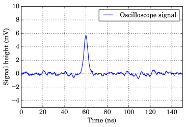
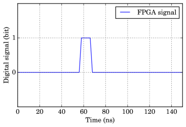
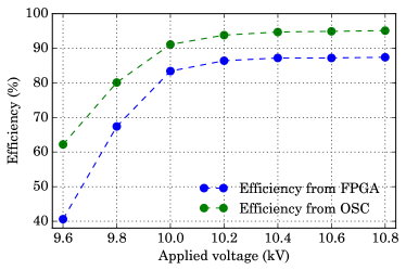
To validate performance of the DAQ system, several measurements have been carried out to study the response of a single strip of the glass RPC prototype. The finger-shaped SCN1 has been aligned along a particular readout strip while the paddle-shaped SCN3 has been placed below the RPC covering the whole active area. The trigger has been generated from the two-fold coincidence of SCN1 and SCN3 to ensure the detection of muon events by the single readout strip. A comparative study has been made between a typical analog signal from the readout strip captured in oscilloscope and the same acquired through the present DAQ system comprising of NINO at the FEE and MAX®-10 FPGA at the BEE stages respectively. The spectra have been depicted in figure LABEL:fig:osc_signal and LABEL:fig:fpga_osc. The figure LABEL:fig:time_hist_fpga has shown a typical distribution of the TOT outputs of the readout strip for muon events as acquired by the present DAQ system. The efficiency of the strip of muon detection with respect to the scintillators has been determined by dividing the muon counts obtained from the strip by the number of triggers generated. In figure LABEL:fig:efficiency, the efficiency as measured by using standard electronics and the present DAQ system has been depicted for different working voltage. It shows that the efficiency determined by using the present DAQ system is less than the other measurement by 7-8% at higher voltages. The possible reason may be due to the use of a threshold 100fC used in the NINO-board for producing the TOT pulse which has curtailed the valid pulses with smaller charge content. It has been corroborated by larger difference in efficiency at lower operating voltage which has reached to about 35% at the operating voltage 9.6kV.
3.3 Trigger Validation
The DAQ system has been tested and validated by acquiring RPC pulses with different trigger conditions produced by different physical setup and logic of three plastic scintillators (SCN1, SCN2 and SCN3) described earlier in section 3.1. Two different cases of physical setup of the scintillators have been shown in figures LABEL:fig:test_trigger_a and LABEL:fig:test_trigger_b.
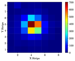
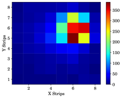
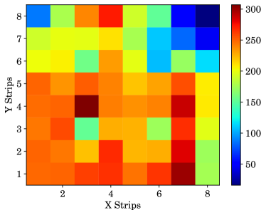
The signals from the RPC for the muon events have been acquired for a logic condition SCN1 & SCN2 & SCN3 from both the cases which are shown in figures LABEL:fig:hit_8x8_pos_1 and LABEL:fig:hit_8x8_pos_2. For the second setup shown in figure LABEL:fig:test_trigger_b, the result of another trigger condition (SCN1 + SCN2) & SCN3 has been illustrated in figure LABEL:fig:hit_8x8_pos_3. The trigger condition in all the cases has been generated when all the three scintillators have generated signals in a coincidence window of 50ns. For each event, a weight factor proportional to the induced charge as indicated by the measured TOT pulse width has been assigned to each strip. In case of n number of strips have fired and produced pulse width , the weight factor assigned to each strip has been calculated as follows.
| (1) |
Thus, when a single strip has been hit, the weight factor assigned to the strip was 1. The position of the event in terms of the strip has been calculated by a weighted sum of the strips for both the readout planes (X,Y). The two-dimensional histograms of the muon events for the given trigger conditions have been illustrated in figure 10 in terms of readout strips.
3.4 DAQ Scalability
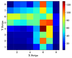
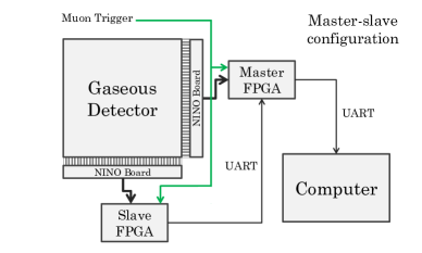
The DAQ system has been tested for its scalability which is an important requirement for building up a tomography setup consisting of multiple muon tracking detectors with larger readout granularity. The present 8 8 readout configuration of the RPC has been operated with different BEE configurations where each of the two NINO-boards of two readout planes (X,Y) has been connected to a MAX®-10 FPGA-board. The FPGA-boards have been configured in master-master and master-slave configuration. The muon trigger has been produced from the coincidence of paddle-shaped SCN3 and a similar one placed above covering the entire active area of the RPC. The trigger has been passed to both of the FPGA-boards simultaneously. The schematic diagram of the experimental setup have been illustrated in figure LABEL:fig:Scalable_DAQ_MM and LABEL:fig:Scalable_DAQ_MS respectively.

A typical muon event histogram obtained with the master-slave configuration has been depicted in figure 12. Events with one, two and three strips hit have been considered for the hit map reconstruction and the events with greater than three strips hit, treated as streamers, have been excluded. This highlights the scalability feature of the DAQ where a 8 8 system can be easily scaled to a 16 16 system or more by adding additional units with very small changes in the software code.
4 Summary & Conclusion
In the present work, we have presented the development of a multi-channel DAQ system to be used for muon tracking using RPC in a MST setup. The FEE stage of the proposed DAQ system has been built around NINO ASIC and the BEE stage has been configured using MAX®-10 FPGA development board. The valid data has been transmitted to an external PC for offline processing through UART. The DAQ system has been tested on a glass RPC for its performance. It has been found capable of direct acquisition of LVDS signals from the FEE stage. The availability of 500MHz sampling frequency on the FPGA-board has offered a timing resolution of 2ns in measuring the TOT pulse provided by the NINO. This has been found fairly acceptable for our application where the main focus is to produce the map of the muon event position. It will also matter a little for a readout strips of 1cm width to be used in future. We have deliberately used a MAX®-10 FPGA development board, in the back-end, instead of a custom-made FPGA board. The custom-made FPGA board usually has a very long development cycle and moreover, it is comparatively costly. In comparison, the readily available development boards are much cheaper and there is no need a long development cycle. Many advantages of a custom-made boards can be achieved by using a modular structure with easy scalability feature. We have demonstrated in section 3.4 that the proposed DAQ has a modular structure that can be easily scaled to accommodate higher number of channels with small modifications in the software code.
Acknowledgements
We are thankful to Mr. Shaibal Saha and other members of our laboratory for assistance and advice for the work. We acknowledge the help extended by the TIFR and INO Collaboration in making NINO-boards and the procurement of FPGA-boards. The author S. Das thanks the UGC, Govt. of India, for financial support.
References
- [1] Pesente et al., First results on material identification and imaging with a large-volume muon tomography prototype, Nuclear Instruments and Methods A 604 (2009) 738.
- [2] C. Morris, C. Alexander, J. Bacon, K. Borozdin, D. Clark, R. Chartrand, C. Espinoza, A. Fraser, M. Galassi, J. Green, et al., Tomographic imaging with cosmic ray muons, Science & Global Security 16 (2008) 37.
- [3] D. F. Mahon et al., A prototype scintillating-fibre tracker for the cosmic-ray muon tomography of legacy nuclear waste containers, Nuclear Instruments and Methods A 732 (2013) 408.
- [4] V. Anghel et al., A plastic scintillator-based muon tomography system with an integrated muon spectrometer, Nuclear Instruments and Meth ods A 798 (2015) 12.
- [5] J. Burns, S. Quillin, M. Stapleton, C. Steer, S. Snow, A drift chamber tracking system for muon scattering tomography applications, Journal of Instrumentation 10 (2015) P10041.
- [6] S. Tripathy, J. Datta, N. Majumdar, S. Mukhopadhyay, Material discrimination in cosmic muon imaging using pattern recognition method, Journal of Instrumentation 15 (2020) P06029.
- [7] V. L. Highland, Some practical remarks on multiple scattering, Nuclear Instruments and Methods in Physics Research 129 (1975) 497.
- [8] G. R. Lynch, O. I. Dahl, Approximations to multiple coulomb scattering, Nuclear Instruments and Methods in Physics Research B 58 (1991) 6.
- [9] J. e. a. P. D. G. Beringer, A study of time over threshold (tot) technique for plastic scintillator counter, Physical Review D 86 (2012) 010001.
- [10] P. Baesso, D. Cussans, C. Thomay, J. J. Velthuis, J. Burns, C. Steer, S. Quillin, A high resolution resistive plate chamber tracking system developed for cosmic ray muon tomography, Journal of Instrumentation 8 (2013) P08006.
- [11] L. Shi, Y. Wang, X. Huang, X. Wang, W. Zhu, Y. Li, J. Cheng, A high time and spatial resolution mrpc designed for muon tomography, Nuclear Instruments and Methods in Physics Research A 652 (2011) 16.
- [12] C. Gnanvo, L. V. Grasso III, M. Hohlmann, J. B. Locke, A. Quintero, D. Mitra, Imaging of high-z material for nuclear contraband detection with a minimal prototype of a muon tomography station based on gem detectors, Journal of Instrumentation 9 (2014) C12038.
- [13] S. Tripathy, J. Datta, N. Majumdar, S. Mukhopadhyay, Numerical evaluation of a muon tomography system for imaging defects in concrete structures, The European Physical Journal Plus 136:824 (2021).
- [14] S. Das, S. Tripathy, P. Jagga, P. Bhattacharya, N. Majumdar, S. Mukhopadhyay, Muography for civil inspection, Instruments 6 (2022) 77.
- [15] S. Das, J. Datta, N. Majumdar, S. Mukhopadhyay, Studies on electrical properties of resistive plate chamber (rpc), Journal of Instrumentation 17 (2022) P09041.
- [16] S. Tripathy, S. Das, J. Datta, N. Majumdar, S. Mukhopadhyay, Precise tracking of cosmic muons using the time-over-threshold property of nino asics, Journal of Instrumentation 15 (2020) C11013.
- [17] F. Anghinolfi, P. Jarron, A. Martemiyanov, E. Usenko, H. Wenninger, M. Williams, A. Zichichi, Nino: an ultra-fast and low-power front-end amplifierdiscriminator asic designed for the multigap resistive plate chamber, Nuclear Instruments and Methods in Physics Research A 533 (2004) 183.
- [18] F. Anghinolfi, P. Jarron, F. Krummenacher, E. Usenko, M. Williams, Nino: An ultrafast low-power front-end amplifier discriminator for the time-of-flight detector in the alice experiment, IEEE Transactions On Nuclear Science 51 (2004) 1974.
- [19] P. K. Kaur, Pathaleswar, M. Saraf, B. Satyanarayana, R. Shinde, Development of fast, low power 8-channel amplifier-discriminator board for the rpcs, Springer Proceedings in Physics 203 (2018) 571.