Strong magnetic proximity effect in Van der Waals heterostructures driven by direct hybridization
Abstract
We propose a new class of magnetic proximity effects based on the spin dependent hybridization between the electronic states at the Fermi energy in a non-magnetic conductor and the narrow spin split bands of a ferromagnetic insulator. Unlike conventional exchange proximity, we show this hybridization proximity effect has a very strong influence on the non-magnetic layer and can be further modulated by application of an electric field. We use DFT calculations to illustrate this effect in graphene placed next to a monolayer of CrI3, a ferromagnetic insulator. We find strong hybridization of the graphene bands with the narrow conduction band of CrI3 in one spin channel only. We show that our results are robust with respect to lattice mismatch and twist angle variations. Furthermore, we show that an out-of-plane electric field can be used to modulate the hybridization strength, paving the way for applications.
Proximity effects in hybrid systems transfer an electronic property, intrinsic to a certain material, to an adjacent material in which that property is absent. For example, the surface of a material that otherwise has no electronic order can become superconducting, or magnetic, when placed in contact with superconductors or a ferromagnet. Proximity effects are an important resource in the design of quantum matter in artificial heterostructures. For instance, topological superconductivity can be induced by taking advantage of either the superconducting proximity effect in semiconducting nanowires Lutchyn et al. (2010) or magnetic proximity effects on a superconductor surface Nadj-Perge et al. (2014).
With the advent of two-dimensional (2D) materials Geim and Novoselov (2005); Castellanos-Gomez (2016); Frisenda et al. (2018), proximity effects have become particularly relevant since they can alter the electronic properties of an entire crystal. The discovery of ferromagnetic 2D crystals Huang et al. (2017), such as CrI3, and the demonstration of Van der Waals heterostructures that combine them with non-magnetic 2D crystals Klein et al. (2018); Huang et al. (2017), motivate the present work. Specifically, there are now several experimental papers exploring the spin proximity effects induced by Van der Waals ferromagnetic insulators on non-magnetic 2D crystals, including semiconductors Zhong et al. (2017); Norden et al. (2019); Lyons et al. (2020), graphene Tang et al. (2020); Ghiasi et al. (2020); Wu et al. (2021); Lyu et al. (2022) and superconductors Kezilebieke et al. (2020); Kang et al. (2021), as well as other exciting possibilities, such as 2D ferromagnetic metals in contact with antiferromagnetic insulators Zhang et al. (2020), and Kitaev materials in contact with graphene Mashhadi et al. (2019).
The ferromagnetic proximity effect is most often modeled by adding spin-splitting to the bands of the non-magnetic material to account for exchange interaction with a ferromagnet. In van der Waals materials density functional theory (DFT) calculations predict values of the proximity exchange splitting as large as 70 meV Qiao et al. (2014), whereas the values reported experimentally are rather small, with induced spin splittings typically in the range of few meV. These yield interesting but modest changes in the optical Zhong et al. (2017); Norden et al. (2019) and transport Tang et al. (2020); Ghiasi et al. (2020) properties of the non-magnetic material. Here we propose a complementary type of spin proximity effect, based on spin-dependent hybridization of the bands of a conducting material with those of a spin-split insulating ferromagnet. This type of proximity effect is always relevant when charge transfer occurs between magnetic and non-magnetic layers, and we show that it can have a radical impact in the properties of the non-magnetic material. Importantly, it can be tuned electrically, opening the door to new device concepts.
The proposed hybridization proximity effect arises from the spin dependent coupling between the atomic orbitals that form the conduction band of the conducting material and a set of localized spin split states in the ferromagnet. In many cases it will significantly alter the energy bands and the mobility of only one of the spin channels of the conductor. Hybridization proximity occurs when a spin-split band of the ferromagnetic insulator is aligned with the Fermi energy of the conductor but, as we discuss below, this resonant condition occurs naturally by self-alignment of bands in a wide class of magnetic insulators.
To be explicit we consider in the following the case of the two dimensional conductor graphene, in proximity with a ferromagnetic insulator, like CrI3 (see Figure 1). The essence of the proposed effect is independent of the dimensionality of both the magnetic and the non magnetic material, but the consequences will be more dramatic when the non-magnetic materials is two dimensional, and the magnetic insulator is sufficiently thin to allow integration in a dual gate structure with top and bottom gate electrodes.
The microscopic principle of the hybridization proximity effect can be discussed in terms of a two band model Hamiltonian which neglects spin-orbit coupling. The spin Hamiltonian
| (1) |
where is the spin-independent band dispersion of the non-magnetic conductor, is the spin dependent energy band of the insulating ferromagnet and is interlayer hybridization between these two bands. In ferromagnetic insulators both the conduction and the valence band can have either majority or minority spin. Interlayer coupling leads to two types of effects in the non-magnetic material. First, away from the narrow energy window where the bands of the ferromagnetic material lie, hybridization leads to a perturbatively small spin-splitting given by
| (2) |
Second, in the energy window where the bare bands of both materials are degenerate, there is strong hybridization that opens up a gap. Since , this gap only occurs in one spin channel, at a given energy. Thus, if the Fermi energy lies in one of these resonance windows, the spin polarization of the conductor is effectively 100%.
We now make two crucial observations. First, charge transfer occurs at the interface of the 2D conductor and the magnetic insulator when the difference in work functions is larger than the insulator’s gap. As a result, either the valence or the conduction band of the magnetic insulator has to self-align with the Fermi energy of the conductor. For this reason the hybridization proximity effect is relevant in a wide class of magnetic insulators, with spin polarized valence or conduction band. This is the central point of this work. Second, exact alignment between bands of the conductor and the magnetic insulator can be further tuned by application of an electric field perpendicular to the interface, which can result in a strong change in the strength of the hybridization proximity effect and therefore in a modulation of the spin splitting (Eq. 2).
The electrostatics of the interface are roughly described by the Wigner-Bardeen rule Wigner and Bardeen (1935) which asserts that electrons will be transferred from the material with the smallest work function to the material with the largest work function . When the difference in work function is larger than the energy gap, we can estimate the charge transfer using a parallel plate estimation of the potential drop, in which extra electrons and extra holes are localized in two parallel planes separated at a distance . The areal density of excess carriers per layer, is then related to the work function difference by
| (3) |
where is the electron charge and is the vacuum dielectric constant. Importantly, a finite implies charge injection into the ferromagnetic insulator and, thereby, alignment of its bands with the Fermi energy of the 2D conductor. In the following we substantiate this estimate with first principles DFT calculations for a hetero-bilayer formed by a ferromagnetic insulator, CrI3, and graphene. This system has been studied experimentally Tseng et al. (2022). For the sake of computational simplicity we choose a monolayer of CrI3, but our results would hold for graphene on top of bulk CrI3, given both the local nature of hybridization proximity, which involves predominantly the interaction between adjacent layers.
CrI3 is a ferromagnetic insulator with a majority spin conduction band Soriano et al. (2020). The Cr atoms are embedded in iodine octahedral cages that split the Cr levels into a triplet and an doublet. The Cr oxidation state is +3, so that Cr+3 ions have 3 electrons in the spin majority orbitals that are strongly hybridized with the iodine orbitals to form the valence band Lado and Fernández-Rossier (2017). The conduction band of CrI3 is formed by the spin majority bands, resulting in relatively non-dispersive bands with a large spin-splitting produced by intra-atomic exchange. The work functions of graphene and CrI3 are eV Filleter et al. (2008); Datta et al. (2009); Shi et al. (2009) and eV respectively. Therefore, it is expected that electron transfer occurs from graphene to the conduction band of CrI3 Zhang et al. (2018), self-aligning the narrow spin-split conduction band of CrI3 and the Dirac cones of graphene.
In order to describe the hybridization proximity effect more quantitatively, we now carry out density functional theory simulations using the plane-wave and pseudo-potential implementation provided by the Quantum-ESPRESSO package Giannozzi et al. (2009, 2017). We employed projector augmented wave (PAW) pseudo-potentials, and the Perdew-Burke-Ernzerhoff (PBE) Perdew et al. (1996) exchange-correlation functional with Grimme-D2 Grimme (2006) van der Waals corrections.
We first neglect inter-layer hybridization by solving Kohn-Sham equations for isolated CrI3 and graphene layers, but taking account of the expected electron density transfer from graphene to CrI3. Graphene therefore has hole pockets centered on the and points in momentum space that enclose approximately 1% of its Brillouin zone. We find that CrI3 has six electron pockets located away from the high-symmetry points of the Brillouin zone (BZ) that cover approximately 8% of its much smaller Brillouin-zone area. Strong interlayer hybridization occurs when the Fermi surfaces of the two layers, smeared in energy by , intersect Bistritzer and MacDonald (2011); Shi and MacDonald (2023). In Fig. 2 we plot the graphene and CrI3 Fermi surfaces reduced to the first BZ of graphene, for different twist angles. It is apparent that, for most angles, the graphene Fermi surface pockets are very close or right on top some Cr pockets. Therefore, we expect a moderate dependence of the interlayer hybridization on twist angle in this system.


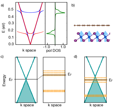
In order to support the above qualitative analysis for incommensurate CrI3/graphene bilayers, we carried out a DFT calculation for the coupled bilayer with a low-order commensurate unit cell. We consider a 55 graphene supercell with Å (instead of Å obtained for isolated graphene) on top of a suitably oriented CrI3 supercell with Å (instead of Å). The resulting energy bands for the CrI3/graphene VdW structure are shown in Fig. 3c). As expected from the argument above, the spin minority channel (in red) shows only the pristine graphene Dirac cone, since the spin majority states of CrI3 are far away in energy. In contrast, in the spin majority channel (in blue) in the graphene cone is strongly hybridized with the CrI3 conduction band shown in grey. In this situation, we expect a strong spin dependence of the electronic transport: whereas spin-minority channel has a pristine Dirac cone, the graphene states of the spin majority channel are scrambled with the narrow conduction band of CrI3. Given the Mott insulating nature of CrI3 McGuire et al. (2015), conduction in the spin majority channel is very likely strongly suppressed, compared with the spin minority graphene Dirac cone. This dramatically different landscape for the two spin channels at the Fermi energy constitutes the essence of the hybridization spin-proximity effect.
We now turn our attention to how to electrically control the band alignment between the non-magnetic conductor and the magnetic insulator. The band alignment is controlled by the magnitude of the charge transfer. The vertical shift of the bands at both sides, estimated with a jellium model in the Hartree approximation, would be given by , where is the areal density of transferred electrons which has opposite signs for opposite layers. So, if we apply an out-of-plane electric field to compensate for the electrochemical charge transfer, this will reduce , and thereby will push the (hole rich) graphene layer down in energy and the (electron rich) magnetic insulator layer up in energy. Application of an electric field, for example with a single back-gate, would also inject additional carriers into the graphene/magnetic insulator bilayer. This can be avoided using a dual gate device Zhang et al. (2009); Taychatanapat and Jarillo-Herrero (2010) which permits one to independently control the carrier injection and the voltage drop at the bilayer.
Our DFT calculations with no applied electric field show that charges accumulate in the carbon atoms and in the iodine atoms of the top layer. From DFT we also obtain an average distance between C and I of d=3.54 Å. Using Eq. 3 we estimate the areal density of electron that transfer from graphene to CrI3, . From DFT, we obtain a value of the integrated charge difference of 0.9 cm-2, not far from the simple model estimate.
We have also carried out DFT calculations with an out-of-plane electric field. Since the charge in the system remains constant, our calculations describe an experimental situation where top and bottom gate voltages are chosen so as to make the carrier injection zero Lei et al. (2021). The evolution of the energy bands for the Gr/CrI3 heterobilayer as a function of electric field are shown in Fig. 4. We consider fields up to E=100 meV/Å, close to the limit that can be achieved without reaching dielectric breakdown. The polarity of the field is chosen to reduce the charge transfer that occurs spontaneously at the Gr/CrI3 interface. Therefore the displacement field moves electrons back from the conduction band of CrI3 to graphene. As a result, the conduction band has to shift upwards in energy, relative to the graphene Dirac cone, as shown in Fig. 4d).

Our calculations show that, as we ramp the electric field, the energy bands at the Fermi energy go from a strong hybridization regime in which we expect the bilayer to behave as a half-metal, towards a regime dominated by spin-split graphene Dirac cones, with the flat bands of CrI3 higher in energy and disentangled from those of graphene. In the second case, both spin channels of graphene will contribute to its conductance, increasing its value by a factor of two. In parallel with the increase in conductance, the spin polarization at the Fermi energy decreases.
Interestingly, in the non-resonant regime, the spin splitting of the Dirac cones does depend on the electric field. The effective interlayer exchange is ferromagnetic, as the sign of the spin splitting is the same for the graphene and CrI3 bands. As expected from Eq. (2), as we increase the field, pulling apart the CrI3 bands from the Dirac point states, the magnitude of the splitting goes down. Thus, the splitting can be controlled electrically, and keeping the interface in the non-resonant regime, it can be tuned from 48 meV at zero field, to 28 meV for a field of 100 meV/Å. The smooth crossover from the hybridization towards the conventional spin proximity effect highlight that both are generated by the same underlying mechanism, namely, the hybridization of the non-magnetic states with spin split states of the ferromagnet.
The hybridization proximity effect is by no means specific to CrI3. First, it can be anticipated other magnetic insulators with magnetic ions with a less than half-full d-shells in a octahedral environment, such as CrBr3, CrCl3, VX3 (X=I, Br, C), CrBrS also have majority spin spin-polarized conduction bands. In addition, previous computational work modelling graphene on top of magnetic insulators, such as CrBr3 Behera et al. (2019); Lyu et al. (2022), CrI3 Zhang et al. (2018); Cardoso et al. (2018), RuCl3 Mashhadi et al. (2019); Rizzo et al. (2020), FeCl3 Wei-Bang et al. (2020) show spin-dependent hybridization of the graphene bands and self-alignment with the spin-split conduction bands of these materials.
In summary, we propose that a strong proximity effect that occurs when a magnetic insulator is placed in proximity with graphene. The effect is the consequence of spin-selective hybridization of the states at the Fermi surface of the conductor with a spin polarized band of the ferromagnet. The energy of the two types of bands naturally aligns when charge is transferred at the interface to compensate for the work function difference. We claim this will occur naturally when graphene is placed on a variety of magnetic insulators with spin polarized conduction bands. We also show that the strength of hybridization magnetic proximity can be further tuned by application of an off-plane electric field. Our DFT calculations of the Van der Waals heterostructure Gr/CrI3 confirm the theoretical scenario.
Acknowledgments This work was partially supported by MaX – MAterials design at the eXascale – a European Centre of Excellence funded by the European Union’s program HORIZON-EUROHPC-JU-2021-COE-01 (Grant No. 101093374). JFR and AC acknowledge financial support from FCT (Grant No. PTDC/FIS-MAC/2045/2021), the Swiss Science National Foundation Sinergia (Grant Pimag), the European Union (Grant FUNLAYERS - 101079184). JFR acknowledges funding from FEDER /Junta de Andalucía, (Grant No. P18-FR-4834), Generalitat Valenciana funding Prometeo2021/017 and MFA/2022/045, and funding from MICIIN-Spain (Grant No. PID2019-109539GB-C41). AHM was supported by the U.S. Department of Energy, Office of Science, Basic Energy Sciences, under Award No. DE-SC0022106.
References
- Lutchyn et al. (2010) R. M. Lutchyn, J. D. Sau, and S. D. Sarma, Physical review letters 105, 077001 (2010).
- Nadj-Perge et al. (2014) S. Nadj-Perge, I. K. Drozdov, J. Li, H. Chen, S. Jeon, J. Seo, A. H. MacDonald, B. A. Bernevig, and A. Yazdani, Science 346, 602 (2014).
- Geim and Novoselov (2005) A. K. Geim and K. S. Novoselov, Nature Materials 6, 183 (2005).
- Castellanos-Gomez (2016) A. Castellanos-Gomez, Nature Photonics 10, 202 (2016).
- Frisenda et al. (2018) R. Frisenda, E. Navarro-Moratalla, P. Gant, D. P. De Lara, P. Jarillo-Herrero, R. V. Gorbachev, and A. Castellanos-Gomez, Chemical Society Reviews 47, 53 (2018).
- Huang et al. (2017) B. Huang, G. Clark, E. Navarro-Moratalla, D. R. Klein, R. Cheng, K. L. Seyler, D. Zhong, E. Schmidgall, M. A. McGuire, D. H. Cobden, W. Yao, D. Xiao, P. Jarillo-Herrero, and X. Xu, Nature 546, 270 (2017).
- Klein et al. (2018) D. R. Klein, D. MacNeill, J. L. Lado, D. Soriano, E. Navarro-Moratalla, K. Watanabe, T. Taniguchi, S. Manni, P. Canfield, J. Fernández-Rossier, and P. Jarillo-Herrero, Science 360, 1218 (2018).
- Zhong et al. (2017) D. Zhong, K. L. Seyler, X. Linpeng, R. Cheng, N. Sivadas, B. Huang, E. Schmidgall, T. Taniguchi, K. Watanabe, M. A. McGuire, et al., Science advances 3, e1603113 (2017).
- Norden et al. (2019) T. Norden, C. Zhao, P. Zhang, R. Sabirianov, A. Petrou, and H. Zeng, Nature communications 10, 1 (2019).
- Lyons et al. (2020) T. P. Lyons, D. Gillard, A. Molina-Sánchez, A. Misra, F. Withers, P. S. Keatley, A. Kozikov, T. Taniguchi, K. Watanabe, K. S. Novoselov, et al., Nature communications 11, 1 (2020).
- Tang et al. (2020) C. Tang, Z. Zhang, S. Lai, Q. Tan, and W.-b. Gao, Advanced Materials 32, 1908498 (2020).
- Ghiasi et al. (2020) T. S. Ghiasi, A. A. Kaverzin, A. H. Dismukes, D. K. de Wal, X. Roy, and B. J. van Wees, arXiv preprint arXiv:2007.15597 (2020).
- Wu et al. (2021) Y. Wu, Q. Cui, M. Zhu, X. Liu, Y. Wang, J. Zhang, X. Zheng, J. Shen, P. Cui, H. Yang, et al., ACS Applied Materials & Interfaces 13, 10656 (2021).
- Lyu et al. (2022) P. Lyu, J. Sødequist, X. Sheng, Z. Qiu, A. Tadich, Q. Li, M. T. Edmonds, J. Redondo, M. Švec, T. Olsen, et al., arXiv preprint arXiv:2212.02772 (2022).
- Kezilebieke et al. (2020) S. Kezilebieke, M. N. Huda, V. Vaňo, M. Aapro, S. C. Ganguli, O. J. Silveira, S. Głodzik, A. S. Foster, T. Ojanen, and P. Liljeroth, Nature 588, 424 (2020).
- Kang et al. (2021) K. Kang, S. Jiang, H. Berger, K. Watanabe, T. Taniguchi, L. Forró, J. Shan, and K. F. Mak, arXiv preprint arXiv:2101.01327 (2021).
- Zhang et al. (2020) L. Zhang, X. Huang, H. Dai, M. Wang, H. Cheng, L. Tong, Z. Li, X. Han, X. Wang, L. Ye, et al., Advanced Materials , 2002032 (2020).
- Mashhadi et al. (2019) S. Mashhadi, Y. Kim, J. Kim, D. Weber, T. Taniguchi, K. Watanabe, N. Park, B. Lotsch, J. H. Smet, M. Burghard, et al., Nano Letters 19, 4659 (2019).
- Qiao et al. (2014) Z. Qiao, W. Ren, H. Chen, L. Bellaiche, Z. Zhang, A. MacDonald, and Q. Niu, Physical review letters 112, 116404 (2014).
- Wigner and Bardeen (1935) E. Wigner and J. Bardeen, Phys. Rev. 48, 84 (1935).
- Tseng et al. (2022) C.-C. Tseng, T. Song, Q. Jiang, Z. Lin, C. Wang, J. Suh, K. Watanabe, T. Taniguchi, M. A. McGuire, D. Xiao, et al., Nano Letters (2022).
- Soriano et al. (2020) D. Soriano, M. I. Katsnelson, and J. Fernández-Rossier, Nano Letters 20, 6225 (2020).
- Lado and Fernández-Rossier (2017) J. L. Lado and J. Fernández-Rossier, 2D Materials 4, 035002 (2017).
- Filleter et al. (2008) T. Filleter, K. V. Emtsev, T. Seyller, and R. Bennewitz, Applied Physics Letters 93, 133117 (2008).
- Datta et al. (2009) S. S. Datta, D. R. Strachan, E. J. Mele, and A. T. C. Johnson, Nano Letters 9, 7 (2009).
- Shi et al. (2009) Y. Shi, X. Dong, P. Chen, J. Wang, and L.-J. Li, Phys. Rev. B 79, 115402 (2009).
- Zhang et al. (2018) J. Zhang, B. Zhao, T. Zhou, Y. Xue, C. Ma, and Z. Yang, Physical Review B 97, 085401 (2018).
- Giannozzi et al. (2009) P. Giannozzi, S. Baroni, N. Bonini, M. Calandra, R. Car, C. Cavazzoni, D. Ceresoli, G. L. Chiarotti, M. Cococcioni, I. Dabo, et al., J. Phys.: Condens. Matter 21, 395502 (2009).
- Giannozzi et al. (2017) P. Giannozzi, O. Andreussi, T. Brumme, O. Bunau, M. Buongiorno Nardelli, M. Calandra, R. Car, C. Cavazzoni, D. Ceresoli, M. Cococcioni, N. Colonna, I. Carnimeo, A. Dal Corso, S. de Gironcoli, P. Delugas, R. A. DiStasio Jr., A. Ferretti, A. Floris, G. Fratesi, G. Fugallo, R. Gebauer, U. Gerstmann, F. Giustino, T. Gorni, J. Jia, M. Kawamura, H.-Y. Ko, A. Kokalj, E. Küçükbenli, M. Lazzeri, M. Marsili, N. Marzari, F. Mauri, N. L. Nguyen, H.-V. Nguyen, A. O. de-la Roza, L. Paulatto, S. Poncé, D. Rocca, R. Sabatini, B. Santra, M. Schlipf, A. P. Seitsonen, A. Smogunov, I. Timrov, T. Thonhauser, P. Umari, N. Vast, X. Wu, and S. Baroni, J. Phys.: Condens. Matter 29, 465901 (2017).
- Perdew et al. (1996) J. P. Perdew, M. Ernzerhof, and K. Burke, The Journal of Chemical Physics 105, 9982 (1996).
- Grimme (2006) S. Grimme, Journal of Computational Chemistry 27, 1787 (2006).
- Bistritzer and MacDonald (2011) R. Bistritzer and A. H. MacDonald, Proceedings of the National Academy of Sciences 108, 12233 (2011).
- Shi and MacDonald (2023) J. Shi and A. MacDonald, arXiv preprint arXiv:2305.12116 (2023).
- McGuire et al. (2015) M. A. McGuire, H. Dixit, V. R. Cooper, and B. C. Sales, Chemistry of Materials 27, 612 (2015).
- Zhang et al. (2009) Y. Zhang, T.-T. Tang, C. Girit, Z. Hao, M. C. Martin, A. Zettl, M. F. Crommie, Y. R. Shen, and F. Wang, Nature 459, 820 (2009).
- Taychatanapat and Jarillo-Herrero (2010) T. Taychatanapat and P. Jarillo-Herrero, Physical review letters 105, 166601 (2010).
- Lei et al. (2021) C. Lei, B. L. Chittari, K. Nomura, N. Banerjee, J. Jung, and A. H. MacDonald, Nano Letters 21, 1948 (2021).
- Behera et al. (2019) S. K. Behera, M. Bora, S. S. P. Chowdhury, and P. Deb, Physical Chemistry Chemical Physics 21, 25788 (2019).
- Cardoso et al. (2018) C. Cardoso, D. Soriano, N. García-Martínez, and J. Fernández-Rossier, Physical Review Letters 121, 067701 (2018).
- Rizzo et al. (2020) D. J. Rizzo, B. S. Jessen, Z. Sun, F. L. Ruta, J. Zhang, J.-Q. Yan, L. Xian, A. S. McLeod, M. E. Berkowitz, K. Watanabe, et al., arXiv preprint arXiv:2007.07147 (2020).
- Wei-Bang et al. (2020) L. Wei-Bang, L. Shih-Yang, T. Ming-Shuei, L. Ming-Fa, and L. Kuang-I, arXiv preprint arXiv:2012.14648 (2020).