Niobium Quantum Interference Microwave Circuits
with Monolithic Three-Dimensional (3D) Nanobridge Junctions
Abstract
Nonlinear microwave circuits are key elements for many groundbreaking research directions and technologies, such as quantum computation and quantum sensing. The majority of microwave circuits with Josephson nonlinearities to date is based on aluminum thin films, and therefore they are severely restricted in their operation range regarding temperatures and external magnetic fields. Here, we present the realization of superconducting niobium microwave resonators with integrated, three-dimensional (3D) nanobridge-based superconducting quantum interference devices. The 3D nanobridges (constriction weak links) are monolithically patterned into pre-fabricated microwave LC circuits using neon ion beam milling, and the resulting quantum interference circuits show frequency tunabilities, flux responsivities and Kerr nonlinearities on par with comparable aluminum nanobridge devices, but with the perspective of a much larger operation parameter regime. Our results reveal great potential for application of these circuits in hybrid systems with e.g. magnons and spin ensembles or in flux-mediated optomechanics.
Introduction
Superconducting microwave circuits with integrated Josephson junctions (JJs) and superconducting quantum interference devices (SQUIDs) have led to groundbreaking experimental and technological developments in recent decades. Both, single JJs and SQUIDs constitute a flexible and designable Josephson or Kerr nonlinearity, while a SQUID additionally provides in-situ tunability of the resonance frequency by external magnetic flux. Circuits with large nonlinearities originating from the Josephson element form artificial atoms and qubits [4, 5], which have been used for spectacular experiments in circuit quantum electrodynamics [6] and quantum information processing [7]. Frequency-tunable devices with a small nonlinearity are highly relevant for quantum-limited Josephson parametric amplifiers [8, 9, 10], tunable microwave cavities for hybrid systems with spin ensembles and magnons, for dispersive SQUID magnetometry [11, 12], for photon-pressure systems [13, 14, 15] and for microwave optomechanics [17, 18, 19, 20].
In many of these currently active research fields, such as flux-mediated optomechanics, hybrid quantum devices with magnonic oscillators and dispersive SQUID magnetometry, it is highly desirable to have frequency-tunable microwave circuits with small nonlinearity, high magnetic field tolerance and (in some cases) a critical temperature significantly above that of aluminum. The vast majority of frequency-tunable and nonlinear circuits, however, uses Josephson junctions and SQUIDs made of aluminum thin films [21, 22], a superconducting material with a critical magnetic field of only mT (depending on material properties) and a critical temperature K. An approach that could fulfil the aforementioned wishlist is the implementation of microwave circuits made of niobium [23], niobium alloys [24, 25] or even a high- superconductor such as YBCO [26, 27, 28] with high critical current density and high-field compatible Josephson elements such as nano-constrictions [29, 30, 31]. In most efforts so far, however, it has been proven difficult to obtain large-tunability constriction-junction SQUIDs made of these materials, both in direct current (DC) operation mode and in the microwave domain [30, 32, 33, 34, 35].
Here, we report the realization of niobium superconducting quantum interference microwave circuits based on focused neon-ion-beam patterned monolithic 3D nanobridge junctions. Although the SQUIDs in our devices have a large effective area of µm2, we achieve smaller screening parameters than previous 2D niobium nanobridge SQUID circuits with much smaller loops [30]. A small screening parameter is an important prerequisite for stable flux-tunability of the circuit resonance frequency and large flux responsivities [36]. In addition, we characterize our nanobridge quantum interference circuits at varying temperatures in the regime KK and demonstrate that they have only a small Kerr nonlinearity of kHz, ideal for large dynamic range applications. Our devices and results show great potential for dispersive SQUID magnetometry, hybrid systems with spin ensembles, magnons or cold atoms and for flux-mediated optomechanics.
Devices
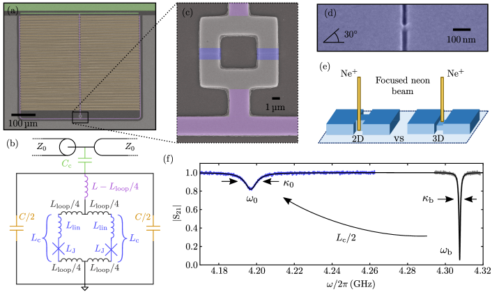
Our devices are lumped element microwave circuits, patterned from a nm thick layer of magnetron sputtered niobium on top of a high-resistivity silicon substrate with thickness µm. They consist of two interdigitated capacitors (IDC) combined in parallel and several linear inductors, and they are capacitively side-coupled to a coplanar waveguide transmission line by means of a coupling capacitance for driving and readout. One of the devices and its circuit equivalent are shown in Fig. 1(a) and (b), respectively. The width of all lines (fingers and inductor wires) and the gaps in between two adjacent IDC fingers is µm. At the connection point between the capacitors and the inductor wires, a square-shaped loop with an effective area of µm2 (hole size µm2) is embedded into the circuit, which forms the SQUID once the nano-constrictions are introduced, cf. Fig. 1(c, d).
After patterning the circuit itself by means of optical lithography and reactive ion etching using SF6, the nano-constrictions are fabricated into the center of the two loop arms using a focused neon ion beam. For the simplest constrictions, we cut a narrow nm wide slot from both sides into each of the two loop arms, leaving only a nm wide constriction in the center of each arm. This type of constriction (thickness equal for the leads and the constriction) has been referred to as 2D constriction and has been implemented for both, DC and microwave SQUIDs [32, 33, 30]. It has also been demonstrated, however, that 3D versions, i.e., constrictions that are thinner than the superconducting leads connected to them, can have superior properties such as less skewed current-phase-relations and smaller critical currents [32, 37, 38]. Implementing 3D constrictions allows for keeping the circuit film thickness large, i.e., the circuit and loop kinetic inductance small, while at the same time getting a critical junction current µA, a highly desirable range for simultaneously achieving a large frequency tunability and a small circuit nonlinearity. For the implementation of the 3D versions, we therefore modify our ion beam scan pattern in a way that the constriction is thinned down during the cutting procedure, cf. Fig. 1(e), more details can be found in Supplementary Note I. Such a monolithic approach for the generation of 3D nanobridges circumvents some of the challenges and possible problems of previously implemented multi-layer deposition processes, such as guaranteeing good galvanic contact between the layers or dealing with thin additional edges at the bottom of the microwave structures [37, 38]. Furthermore, it allows for the unique opportunity to characterize one and the same microwave circuit both without and with the junctions, i.e., one can determine experimentally the impact of the junctions on the circuit properties.
We combine several LC circuits on a single coplanar waveguide feedline, more specifically four circuits with a SQUID and three circuits without a SQUID for reference. The base circuits only differ in the number of fingers in the IDCs and in the corresponding resonance frequencies between and GHz. We present data for three of the SQUID resonators with three different constriction types; one resonator has 2D constrictions (junction thickness nm) and two resonators have 3D constrictions with nm (3D1) and with nm (3D2), respectively (thicknesses are estimated from the neon dose). The total chip is mm2 large and is mounted into a printed circuit board (PCB), to which both the ground planes and the coplanar waveguide feedlines are connected through wirebonds. Chip and PCB are placed in a radiation-tight copper housing and the package – including a magnet coil fixed to the box – is mounted into the vacuum chamber of a dipstick that can be inserted into a liquid Helium cryostat. The cryostat allows for a high-stability temperature control in the range KK by a combination of pumping on the liquid helium container and a feedback loop using a temperature diode and a heating resistor in the vacuum compartment where the sample is mounted. The sample box including the magnet is placed additionally into a cryoperm magnetic shield and the whole cryostat is packed into a double-layer room temperature mu-metal shield. The microwave input line is strongly attenuated with dB to equilibrate the incoming noise to the sample temperature and the output line is connected to a cryogenic high-electron-mobility-transistor amplifier. More details on the experimental setup are given in Supplementary Notes II and III.
Results - Impact of junction cutting
As first step in our device characterization, we measure the transmission coefficient with a vector network analyzer (VNA) once before the constriction patterning and once after. In Fig. 1(f), the transmission at K for the device 3D1 is shown in direct comparison for both cases. From the fits, we obtain the resonance frequencies GHz (no constrictions) and GHz (with constrictions) and therefore can calculate the single-constriction inductance from the constriction-induced frequency shift via
| (1) |
Using pH as obtained from a combination of measuring the temperature-dependence of the resonance frequency and numerical simulations with the software package 3D-MLSI [39], cf. Supplementary Note IV for all device parameters, we get pH for the device 3D1.
Additionally, we extract the internal (subscript ’i’) and external (subscript ’e’) linewidths from the fit before and after nanobridge patterning and obtain kHz, MHz without and MHz, MHz with the constriction junctions. Here and . A change in the external linewidth is most likely due to a slightly different input impedance of the feedline from the resonator perspective before and after the junction cutting and could either be related to a frequency-dependent feedline impedance () or to a change of impedance induced by taking the sample out of the PCB for the cutting and mounting/wirebonding it back into the box afterwards. The considerable increase of the internal linewidth indicates that cutting the junction has introduced an additional loss channel and we believe it is related to an increased quasiparticle density inside the constriction. First, it has been observed that ion-milled constrictions have a reduced critical temperature compared to the rest of the niobium film [40, 41, 42, 43], which locally decreases the superconducting gap and increases the intrinsic thermal quasiparticle density, cf. also the later discussion of the temperature dependence of the devices. Based on this reduced gap, the local quasiparticle density could even be further increased, since the constriction with the reduced gap might act as a potential well or trap for thermal quasiparticles from the leads, similar to what has been observed in aluminum constrictions or vortex cores [44, 45]. We note that the increase of losses could also partly be related to generating some normal-conducting niobium at the surface or at the edges of the constriction by the neon ions. To illuminate the exact loss mechanisms in detail, however, further and dedicated experiments will be necessary in the future.
By performing completely analogous experiments and data analyses for the circuits 2D and 3D2, we extract the corresponding constriction inductances to be pH and pH. More details regarding the three circuits and their basic parameters , , , and can be found in Supplementary Note IV.
Results - Flux dependence
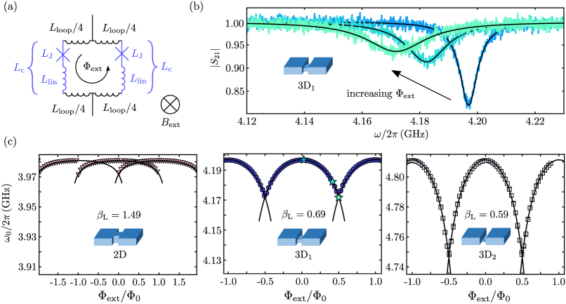
In order to learn more about the nature of the constrictions and how our SQUID circuits perform in terms of frequency-tunability, flux-responsivity and screening parameter, we apply an external magnetic field to the circuits that introduces magnetic flux into the SQUIDs. The constriction inductance we obtained above is not necessarily a purely nonlinear Josephson inductance, but might have a linear contribution as well. In many cases, nano-constrictions have been found to have forward-skewed sinusoidal current-phase relationships (CPRs) [33, 37, 46, 47, 48] and such a skewed sine function can also be modeled approximately as a series combination of an ideal Josephson inductance with sinusoidal CPR and a linear inductance [46], i.e., , cf. Fig. 2(a). Here, the ideal Josephson inductance would be given by , where is the phase difference across the junction, and the critical current of the junction. The Josephson phase of each junction in a symmetric SQUID without bias current is related to the total flux in the loop via . To change the magnetic flux through the loop, we sweep a DC current through the magnet coil attached to the backside of the chip housing, which generates a nearly homogeneous out-of-plane magnetic field at the position of the SQUIDs.
Figure 2(b) shows the circuit response of the 3D1 SQUID circuit for several bias fluxes . We observe that the resonance dip is moving to lower frequencies, i.e., that the resonance frequency is shifted downwards with flux, and that the depth of the dip decreases while the linewidth increases, at least as long as with the flux quantum Tm2. Over larger flux ranges, we in fact observe an oscillating behaviour of the resonance frequency with a periodicity of , reflecting fluxoid quantization in the SQUID loop, cf. Fig. 2(c). Very much as suggested by previous reports [37, 36] and as intuitively expected, we observe that the resonance frequency tuning range (difference between maximum and minimum resonance frequency) gets larger with decreasing constriction thickness. For the 2D junctions (left in Fig. 2(c)), the total resonance frequency tuning range that we can achieve is only on the order of MHz and the individual flux archs strongly overlap with a total observable width of . For the 3D2 device (rightmost in Fig. 2(c)), the tuning range is on the order of MHz and a flux hysteresis (two possible resonance frequencies for a single flux value as in the 2D circuit) is not observable in the data. The 3D1 circuit is somewhere in between, just as it is positioned in Fig. 2(c).
To quantitatively model the flux dependence of the resonance frequency and gather information about and , we consider a flux-dependent resonance frequency
| (2) |
The relation between the total flux in the SQUID and the external flux is given by
| (3) |
where
| (4) |
is the SQUID screening parameter. The result of fitting the flux dependence of the resonance frequency with Eqs. (2) and (3) is shown as lines in Fig. 2(c) and shows good agreement with the experimental data for all three circuits.
The fit parameters we obtain for the single-junction sweetspot inductance , the single-junction critical current , the linear inductance contribution and the screening parameter are summarized in Table. 1. Interestingly, the extracted inductances do not show the somewhat expected tendency that , representing the skewedness of the CPR, decreases with and . As a consequence of the low critical current in the 3D2 device, however, we obtain a small screening parameter despite our large SQUID loop and a maximum flux responsivity MHz, on par with similar aluminum constriction devices [16, 49] and highly promising for applications in photon-pressure systems and flux-mediated optomechanics.
| Circuit | (µA) | (pH) | (pH) | |
|---|---|---|---|---|
| 2D | 65 | 5 | 3 | 1.49 |
| 3D1 | 10 | 33 | 28 | 0.69 |
| 3D2 | 6 | 58 | 45 | 0.59 |
Regarding the increase of the linewidth with flux visible in the data of Fig. 2(b), we believe it is related to a reduction of the superconducting gap with increasing current in the constriction [47], and the corresponding increase in local quasiparticle density, both by the reduction of the gap itself but also by trapping more quasiparticles from the leads. Most likely, there are additional contributions due to internal and external low-frequency flux noise and thermal photon occupation of a nonlinear resonator [22], which at several kelvin is on the order of photons for a GHz mode.
Results - Temperature dependence
An interesting question when characterizing and operating superconducting microwave devices and SQUIDs at a temperature of several ten percent of the critical temperature is how the properties depend on sample temperature in that regime and if we can extrapolate to the properties at lower temperatures from that. The most relevant parameters we are going to consider here are the cavity resonance frequency , the constriction critical current and the SQUID screening parameter for all three circuits.
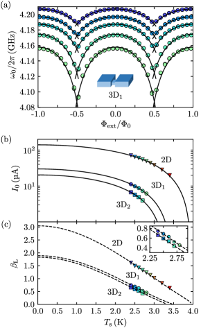
The main results are summarized in Fig. 3. We repeat the experiment of flux-tuning presented in the previous section for different sample temperatures . From the transmission curves for varying external flux we extract , cf. Fig. 3(a) for a corresponding dataset of sample 3D1. Corresponding datasets for 2D and 3D2 can be found in Supplementary Note VIII. For each temperature , we also measured , so we have a reference resonance frequency from before neon irradiation, see also Supplementary Note IV for the temperature dependence of the constriction-less 3D1.
We observe in the resonance frequency tuning-curves that with decreasing temperature the zero-flux resonance frequency gets shifted to larger values, a clear indication for a reduction of the kinetic inductance both in the constrictions and in the rest of the circuit. Furthermore, we find that the tuning range of the resonance frequency is growing with increasing temperature, indicating that the constriction inductance increases faster than the remaining circuit inductance and that the screening parameter decreases, since is increasing faster with than the effective loop inductance .
For a quantification of these effects, we fit the flux-tuning data again with the same equations and procedure as described in the previous section. As a result, we obtain for each sample and , cf. Supplementary Note VIII, and from the former we calculate . The critical currents obtained from this are shown for all three circuits in panel (b). We model the data with the theoretical Bardeen expression for the critical current of a constriction [53, 41]
| (5) |
and find as fitting parameters the critical current at zero temperature as well as the constriction critical temperature . As we already have speculated above, the critical temperature of the constrictions is considerably reduced compared to the niobium film to values between K and K according to these fits. Interestingly, similar s have also been observed for elecron-beam-patterned niobium nanobridges with comparable critical currents [41], therefore the reduced transition temperature might actually not be related to an impact of the neon ions. Since according to this fit our data are taken at , we find that the critical currents still increase by a factor of two in the 2D constrictions and by about a factor of three in the 3D constrictions when approaching and with respect to the smallest experimental temperature K.
It is also interesting to discuss the temperature dependence of and its projected values in the mK regime, although this is a bit speculative due to the limited range of data available. The experimental data shown in Fig. 4(c) for all three circuits have been obtained from the flux-tuning fits. For the 2D sample, the values for are found to be between and in the measured regime and for the 3D samples between and . To model the temperature dependence we take into account the fit curves for as shown in panel (b), the temperature dependence of the loop inductance as discussed in Supplementary Note IV and the temperature dependence of , that we obtain by a fit of the experimentally obtained values, cf. Supplementary Note VIII. We find curves which coincide very well with the experimental data in the measured range of and which predict screening parameters for saturating around for the 2D constrictions and around and for the 3D SQUIDs, respectively.
It seems that the non-sinusoidal CPR of the constrictions is currently the main limiting factor for in the 3D samples, while in the 2D sample pH and the screening parameter is limited by the actual . It will be interesting to see in future experiments in the mK temperature regime if these predictions are valid or if so far neglected effects will emerge and lead to a different behaviour than expected. With lower-temperature experimental possibilities, it will also be interesting to further reduce the thickness and critical current of the 3D junctions, which in the current setup with K was not possible as can be seen from the very limited temperature range already accessible in the existing 3D devices with K.
Results - Kerr nonlinearity of the circuits
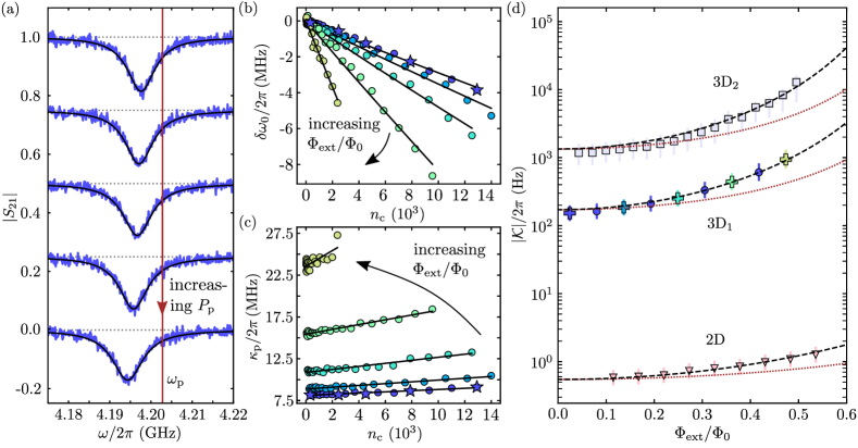
As final experiment we determine a very important parameter of Josephson-based microwave circuits – their Kerr constant , also called anharmonicity or Kerr nonlinearity, which is equivalent to the circuit resonance frequency shift per intracavity photon. For many applications a small Kerr nonlinearity is highly desired, as it increases the dynamic range or maximum intracavity photon number of the device, respectively. This is important for instance in parametric amplifiers [8, 9, 10, 50] and in cavity-based detection techniques such as dispersive SQUID readout [11, 12], SQUID optomechanics [18, 51] and photon-pressure sensing [14, 15], where the signal of interest is proportional to the intracavity photon number and therefore profits from high-power detection tones. The origin of the nonlinearity in our SQUID circuits is the nonlinear inductance of the nano-constrictions. In order to access experimentally, we implement a two-tone protocol, cf. e.g. Refs. [50, 52], and measure the equivalent of the AC Stark shift in the driven circuits. The first microwave tone of the two-tone scheme is a fixed-frequency pump tone with variable power and a frequency slightly blue-detuned from the undriven cavity resonance with . For each pump power, we then measure the pump-dressed device transmission with a small probe tone, cf. Fig. 4(a).
What we find qualitatively in this experiment is that with increasing pump power, the dressed circuit resonance frequency is shifting towards lower frequencies and that the internal linewidth of the mode is increasing, cf. Fig. 4(a). For a quantitative analysis, we fit each pump-dressed resonance with a linear cavity response (cf. Supplementary Note V) for , from which we extract the pump-shifted resonance frequency and the pump-broadened total linewidth .
To model the circuit and the results and to extract , we use the equation of motion for the complex intracavity field
| (6) |
with a nonlinear damping parameter , the total input field and with a normalization such that is the total intracircuit photon number. In the linearized two-tone regime (pump power probe power, details see Supplementary Note VI), we find for the pump-broadened linewidth and the pump-induced frequency shift the relations
| (7) | |||||
| (8) |
Subsequently, we use the and as obtained from the measurements to determine the intracavity photon number for each without any knowledge of , cf. Supplementary Note VI. In panels (b) and (c) of Fig. 4, the extracted values and are shown for various bias flux values and plotted vs the intracircuit pump photon number in device 3D1 at a sample temperature K. Both quantities show a nearly linear dependence on pump photon number as implemented by our model and the corresponding slope depends in turn on the bias flux . We fit the data using Eqs. (7, 8) and obtain for all three devices.
For all circuits, the nonlinearity shown in Fig. 4(d) increases with increasing flux, but the absolute values differ by several orders of magnitude. While the 2D circuit has a Kerr constant of only Hz, the 3D circuits possess nonlinearities of to Hz in 3D1 and up to to Hz in 3D2, respectively. All nonlinearities can still be considered small though and are in particular several orders of magnitude smaller than the cavity linewidths . We observe also very good agreement with the theoretical expression for the Kerr nonlinearity
| (9) |
with the electron charge , the total circuit capacitance , the reduced Planck constant and . Note that we apply the method of nonlinear current conservation discussed in Ref. [50] to obtain this theoretical expression, cf. also Supplementary Note X. The unusual term in the last parenthesis of Eq. (9) is however, not stemming from an asymmetry or a hidden third order nonlinearity, it is a correction factor for perfectly symmetric SQUIDs with screening parameter . How necessary it is to consider this extra term is revealed by the difference to the simple participation ratio expression (Eq. (9) with ), which is also shown in Fig. 4(d) as dotted lines and which for large flux bias values differs from the exact result and the data by up to a factor of .
Discussion
In summary, we have reported and analyzed niobium-based superconducting quantum interference microwave circuits with integrated, monolithically fabricated 2D and 3D nano-constriction SQUIDs. Our results revealed that the tuning range and the flux responsivity of the circuits increases with decreasing constriction thickness and critical current. We have also characterized the Kerr anharmonicity of all circuits and found values between Hz for the 2D circuits up to kHz for the 3D circuit with the lowest critical current junctions. The overall characteristics of the circuits make them highly promising candidates for quantum circuit and quantum sensing applications in particular when high dynamic range and high magnetic fields will be important such as in spin-qubit circuit quantum electrodynamics, hybrid quantum devices with magnonic oscillators or flux-mediated optomechanics.
The most interesting open questions to be investigated in future experiments are the circuit characteristics at temperatures in the mK regime and in large magnetic fields, the exact origin of the microwave losses in the nano-constriction circuits and possibilities to reduce them, as well as a theoretical and experimental investigation of the noise characteristics in such devices. Finally, it will be interesting to investigate possibilities to further reduce the critical currents and the screening parameters, potentially by further reducing the size of the nano-constrictions in all three dimensions.
References
- [1]
- [2]
- [3]