Topological gap protocol based machine learning optimization of Majorana hybrid wires
Abstract
Majorana zero modes in superconductor-nanowire hybrid structures are a promising candidate for topologically protected qubits with the potential to be used in scalable structures. Currently, disorder in such Majorana wires is a major challenge as it can destroy the topological phase and thus reduce the yield in the fabrication of Majorana devices. We study machine learning optimization of a gate array in proximity to a grounded Majorana wire, which allows us to reliably compensate even strong disorder. We propose a metric for optimization that is inspired by the topological gap protocol, and which can be implemented based on measurements of the non-local conductance through the wire.
I Introduction
A promising avenue towards achieving scalable quantum computing involves the utilization of Majorana zero modes (MZMs) [1, 2, 3], which emerge as bound states within topological superconductors [4, 5, 6, 7, 8, 9, 10, 11, 12]. Their occurrence is a consequence of the topological properties of the underlying phase, and they manifest as zero-energy states located within the excitation gap of the system. Due to this topological protection, MZMs exhibit robustness against external perturbations and decoherence. Furthermore, the ability to manipulate MZMs through anyonic braiding allows for the implementation of fault-tolerant qubit operations [4, 5, 6, 7, 13].
MZMs can occur in hybrid systems of conventional superconductors and semiconductors with strong spin-orbit coupling [14, 15, 16, 17, 4]. However, disorder in these systems turns out to be a major problem [18, 19, 20, 21, 22, 23], as it can destroy the topological phase [24] and induce trivial Andreev bound states (ABSs) [25, 26, 27, 28, 29, 30, 31, 32, 33, 34, 35, 36, 37, 38, 39, 40, 41, 42, 43], which can mimic signatures of MZMs [44, 45, 46, 18, 40, 20]. These ABSs complicate the verification of MZMs in experiments as they make more complex measurements and devices necessary [47, 22]. To distinguish MZMs from ABSs, signatures based on coherent transport using electron interferometers [48, 49, 47, 50] are suitable, but experimentally challenging [47]. Another method to detect MZMs is the so-called topological gap protocol [51], which can be applied to a grounded wire contacted with leads at both ends. Here, all elements of the conductance matrix between the two leads are measured to ensure that zero-bias conductance peaks occur simultaneously at both ends and that the excitation gap closes at the boundaries of the topological phase [51].
Numerous experimental studies have confirmed the predicted signatures of Majorana zero modes (MZMs) [52, 53, 54, 55, 56, 57]. Compelling evidence exists for the presence of MZMs in hybrid wires, demonstrated through interferometry [47] and the application of the topological gap protocol [22]. Theoretical investigations have also identified strategies for enhancing MZMs in clean Majorana wires, including the use of magnetic field textures [58, 59, 60, 61], harmonic potential profiles [59], and optimized geometries for Majorana Josephson junctions [62]. However, the presence of disorder in the fabrication process significantly affects the yield of Majorana devices [22], which poses a major limitation for the realization of large-scale qubit systems. Several approaches have been proposed to address this challenge. Firstly, efforts have been made to fabricate cleaner wires by improving fabrication processes [63, 7]. Additionally, it has been demonstrated that weak coupling between superconductors and semiconductors can enhance the resilience of hybrid wires to moderate disorder [64, 65]. Another strategy involves utilizing machine learning optimization techniques to create a potential profile along the Majorana wire using a gate array, compensating for the effects of disorder [66]. However, the optimization process requires the measurement of coherent transport through an electron interferometer [48, 49, 47, 50], which may pose challenges for scalability.
In recent years, the increasing complexity of quantum devices [9, 68, 69, 11, 70] has necessitated the automatic tuning of parameters [71, 72, 73, 74, 75, 76, 77, 78, 79, 80, 81, 82]. Machine learning algorithms have emerged as effective tools for this purpose [83, 73, 77, 84, 70, 79, 81]. In this paper, we propose an optimization approach that employs the CMA-ES machine learning algorithm [67] to tune the voltages on an array of gates located near a Majorana wire. Our optimization metric is based on the principle of the topological gap protocol, eliminating the need for interferometry. We demonstrate the effectiveness of the machine learning algorithm in finding gate voltages that minimize the metric, resulting in the reliable restoration of the topological phase, localized MZMs, and the topological gap, even in the presence of significant disorder. Notably, the optimization process effectively disregards trivial ABSs and can drive the wire from a trivial phase to a topological phase while mitigating the effects of disorder. Additionally, we discuss the convergence properties of the algorithm and argue that this optimization approach is experimentally feasible using currently available technology.
II Setup
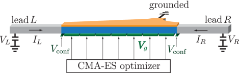
We consider a grounded Majorana hybrid wire of length that is connected to two leads (labeled and ) at the ends (Fig. 1). An array of gates is placed in proximity to the wire such that the voltages on the individual gates can be controlled by the CMA-ES algorithm. Two additional gates that are not included in the optimization are used to separate the wire from the leads by creating a confinement potential.
This setup allows to measure the entries of the conductance matrix between the leads
| (1) |
Denoting the voltage at lead as , the entries in units of at zero temperature are given by [85]
| (2) | ||||
Here, is the number of channels in lead , is the reflection probability for an electron at lead , is the probability for an electron to be reflected as a hole at lead , is the transmission probability for an electron from lead to lead , and is the probability for an electron from lead to be transmitted as a hole to lead [85].
Below, we construct a metric for optimization based on conductance measurements. To assess whether optimization of the metric successfully restores an extended topological phase, we consider the scattering invariant [86]
| (3) |
This is the sign of the determinant of the reflection block obtained from the scattering matrix for lead , containing the complex reflection amplitudes. If the system is in the topological phase holds, and in the trivial phase . However, it is important to note that this scattering invariant is not experimentally accessible and is only reported as a benchmark for assessing the performance of the optimization process for restoring the topological phase.
In order to use MZMs as qubits in a quantum computer, it is not only necessary that the wire is in the topological phase but also that the excitation gap is large. We combine both properties in the so-called topological gap [22], where is the energy of the second level, i.e. the energy of the level above the MZM in the topological phase, which is approximately equal to the excitation gap. To realize qubits, a negative value for the topological gap with large magnitude is advantageous.
For our simulations, we first study an effective one-dimensional wire and consider a more realistic two-dimensional system later. The one-dimensional Majorana wire in Nambu basis is modeled by the BdG Hamiltonian
| (4) |
where is the Rashba spin-orbit coupling strength and is the effective mass of the electrons such that an characteristic energy scale is given by and a characteristic length scale is – realistic values for InAs nanowires [52, 10]. Here, is the proximity induced s-wave superconducting gap, the chemical potential, the Zeeman energy due to an external magnetic field , and and are Pauli matrices acting in spin and particle-hole space, respectively. Disorder in the wire is described by normally distributed random numbers with standard deviation , and a finite correlation length can be introduced by damping high Fourier modes (for details see Appendix A). The confinement potential separating the wire form the leads is given by a steep Gaussian peak at both lead-wire interfaces (see Appendix A). Only when considering tuning a wire from the ABSs regime to the topological phase, we choose a more shallow confinement.
We use the CMA-ES algorithm (for details see Appendix B), which has found many applications for high dimensional optimization problems [87, 88, 89, 90, 91], to optimize the Fourier components of the gate voltages. The Fourier components are related to the voltage on gate via
| (5) |
For reasons of better comparability, we set with the exception of the case where the optimization algorithm tunes from ABSs to MZMs. We assume that the wire is located a distance above the gates such that the potential created by the gate array at position in the wire is given by
| (6) |
Here, and denote Fourier transform and inverse Fourier transform, respectively, and is one for above gate and zero otherwise.
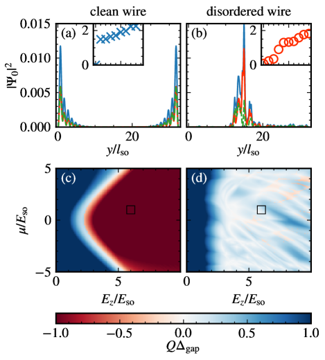
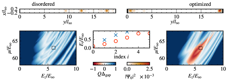
For computing the conductance, the eigenstates, and the energy eigenvalues of the Hamiltonian Eq. (4), we discretize the Hamiltonian on a lattice with spacing , and use the python package KWANT [92] to extract the scattering matrix, the conductance matrix, and the Hamiltonian matrix. As a point of reference, we consider a clean wire in Fig. 2, for which the topological gap shows an extended topological phase as a function of Zeeman field and chemical potential for (red region in panel c) with a gap closing at the boundary (white region in panel c). In the topological phase, there exists a zero energy state in the gap (inset of panel a) with a wave function localized at the wire ends (panel a). For this Majorana wave function , the Majorana condition holds between electron ( in green) and hole components ( in orange). However, when adding strong onsite disorder with standard deviation , the topological phase and the gap are destroyed (panel d). The eigenstate with the smallest energy is no longer localized at the wire ends and does not fulfill the Majorana condition anymore. To compensate the effects of such disorder, in the following, we first introduce a metric and then minimize it by letting the CMA-ES algorithm find optimal gate voltages. As we will demonstrate, this optimization is capable of restoring the topological phase and the Majorana zero mode.
III Metric based on the topological gap protocol
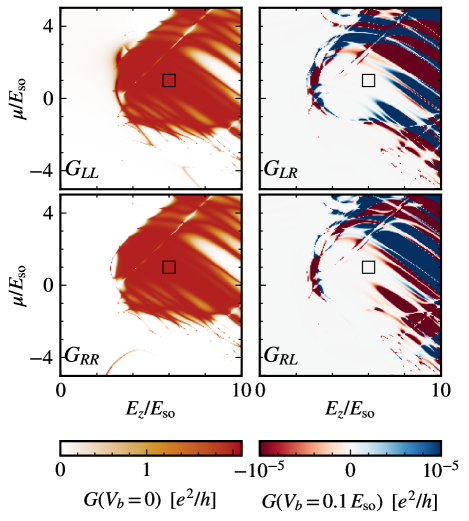
It is crucial for a successful optimization to choose a metric that enhances the desired features when minimized. As disorder can induce trivial ABSs at zero energy, the metric cannot solely rely on the occurrence of zero-bias conductance peaks. We suggest the following metric
| (7) |
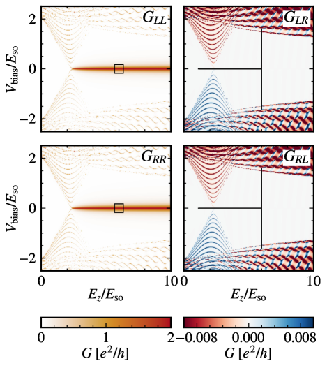
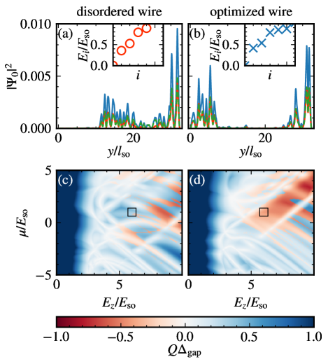
which consists of the following contributions based on the ideas of the topological gap protocol [51], as illustrated for the clean wire in Fig. 3:
-
(i)
As a first contribution the local zero-bias conductance at both loads is measured (left panels). Their product is large if there are localized zero-bias peaks at both ends, as it is the case for localized MZMs.
-
(ii)
As a second contribution, to ensure that the zero-bias peaks are not realized by simply closing the gap, we include an estimator for the transport gap obtained from a scan of the anti-symmetric part of the non-local conductance over a range of bias voltages (black, vertical lines in right panels). This scan is performed by increasing the bias using a step size until the signal peaks at , indicating extended state above the gap. The rescale factor balances the metric such that if the transport gap is the full proximity gap , the contribution to the metric is – the same factor each zero-bias peak would contribute in (i) for ideal MZMs.
-
(iii)
The third contribution involves a scan of the non-local conductances over Zeeman fields in the interval (black, horizontal lines in right panels) with step size , where is the opposite lead of . The contribution to the metric is then given by the logarithm of the maximum of the sum of these non-local conductances, where taking the logarithm ensures that the metric is not dominated by this term as the non-local conductance can change by several orders of magnitude during optimization. This term is large if there is a gap-closing at a Zeeman field in the interval, which is the case if the transition to the topological phase occurs for a Zeeman field smaller than .
Contribution (i) is in analogy to the first region of interest (ROI) of the topological gap protocol while (iii) implements parts of the second phase of the protocol where the gapless part of the boundary of the ROI is determined [51].
IV Optimization of a one-dimensional Majorana wire
We next revisit the Majorana wire of length with strong onsite disorder considered in the right panels of Fig. 2. For a Zeeman energy of and a chemical potential of , we use the CMA-ES algorithm to optimize voltages of gates to minimize the metric Eq. (7) (for optimization with fewer gates see Appendix C). The CMA-ES algorithm is a derivative-free, population based machine learning algorithm [67]: In each step of the optimization a population, i.e. a set of candidate gate voltage configurations, is drawn from a multivariate normal distribution. Then the metric is measured for each candidate in the population. The only information about the physical system that the algorithm needs is the value of the metric for each candidate, and based on the best candidates, the parameters of the algorithm that determine the search region are updated. The idea is that the search region from which the population is drawn can first expand to find candidates close to the minimum and then contract around the minimum. For a detailed description of the CMA-ES algorithm, we refer the reader to Ref. [67] and Appendix B, and details on applying the algorithm to gate array optimization can be found in Ref. [66].
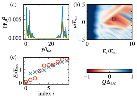
Fig. 4 depicts the Majorana wave function, energy levels, and topological gap when using the optimized gate voltages found by the CMA-ES algorithm. The algorithm is capable of restoring localized MZMs such that the Majorana condition holds again (panel a). A scan of the topological gap through chemical potentials and Zeeman energies (panel b) reveals that optimization not only restores the topological phase at the point of optimization (, ) but for an extended region (shown in red in panel b). In addition, the gap is restored, as can be seen from the comparison of the energy levels before optimization (panel c, red circles) and for the optimized voltages (panel c, blue crosses). These results indicate that the algorithm is indeed able to learn the disorder profile as it found gate voltages such that the potential profile created along the wire compensates the disorder.
We further show that the optimized wire passes the topological gap protocol as it lies in the ROI where zero-bias conductance peaks occur at both ends (Fig. 5, left panels), and the non-local conductances (Fig. 5, right panels) indicate that the boundary of the ROI is gapless, while there is a finite gap within the ROI.
V Inferring the topological invariant from the gap
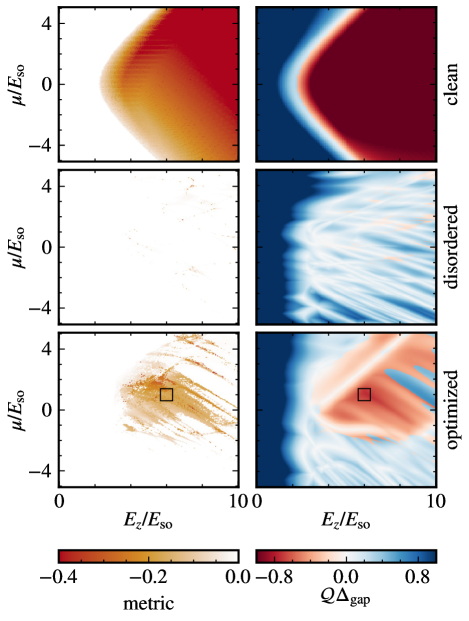
Since the desired properties of the system – the topological phase and a large excitation gap – are encoded in the topological gap , one may assume that it is an ideal metric for optimization. Unfortunately, however, the scattering invariant cannot be accessed experimentally, which disqualifies it for this purpose. To further motivate our metric, Eq. (7), we show a comparison with the topological gap in Fig. 6. For this, we calculate both quantities as a function of chemical potential and Zeeman energy for the clean wire (top panels), the disordered wire with , (center panels), and the disordered wire with optimized gate voltages (bottom panels). We find astonishing agreement between our metric and the topological gap. It turns out that minimizing the metric leads to a topological phase with sizable excitation gap, and the absence of false positives makes the optimization reliable for recovering the topological phase (see also Appendix D for more disorder realizations).
VI Convergence of the optimization
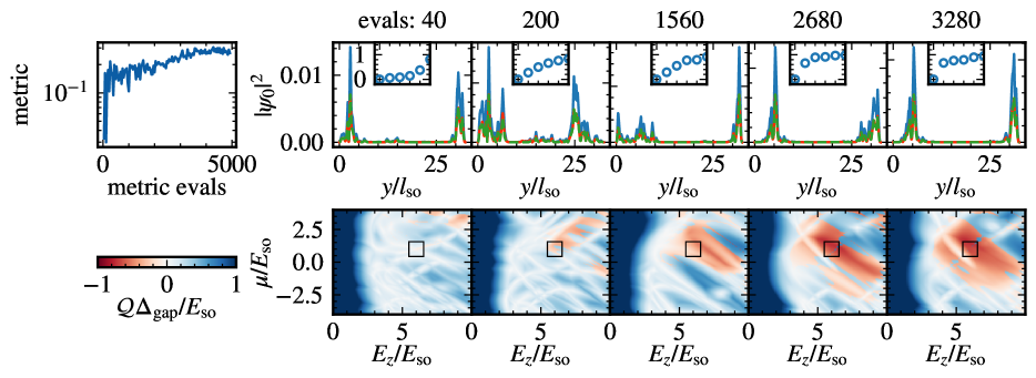
Full convergence of the algorithm, such that for the best gate configurations at step and holds that , may require tens of thousands of calculations (or measurements) of the metric, which would be experimentally very time-consuming. However, our aim is not to achieve full convergence, but to reliably compensate the disorder effects. We therefore consider Majorana wave functions, energy levels, and the topological gap at several steps during the optimization in Fig. 7. The starting point for the optimization is again the disordered wire in the right panel of Fig. 2 with zero voltage on all gates. It becomes apparent that the magnitude of the metric increases rapidly during the initial steps and that the slope subsequently flattens out (upper left panel). After only 40 metric measurements, localized MZMs are recovered at the point . Already after 2680 metric measurements, an extended topological phase with considerable gap is obtained, and after 3280 measurements we no longer observe any significant improvements in the topological gap anymore, although the metric continues to increase slightly. From these observations, we conclude that complete recovery of the MZMs occurs significantly before formal convergence, so that a feasible number of much less than evaluations of the metric is sufficient. In Appendix D, we show further optimizations for various disorder realizations after 3000 metric evaluations and find similar results. In our simulations, one metric evaluation requires in total less than 100 conductance measurements for the scans along Zeeman field and bias voltage.
VII Optimization in the presence of Andreev bound states
The problem of a single conductance measurement is that it cannot distinguish between trivial ABSs pinned at zero energy and topological MZMs. This raises the question whether optimization of the metric, Eq. (7), is able to ignore ABSs and tune the wire into the topological phase while simultaneously compensating for disorder.
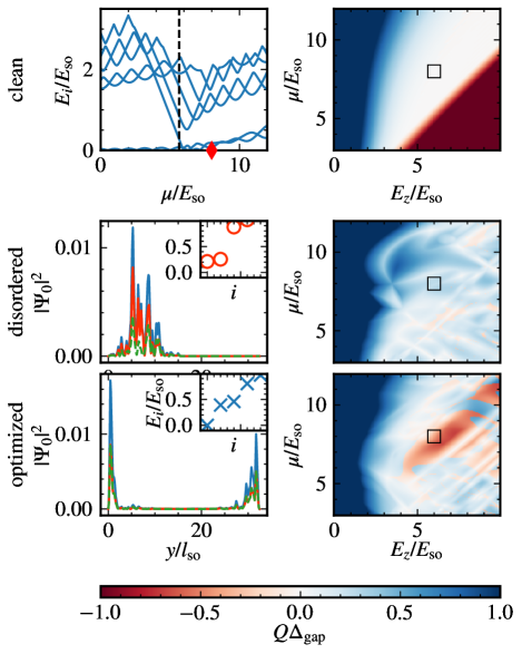
By choosing a smooth confinement potential that slowly decays into the inside of the wire (see Appendix A for details), extended regions with a pair of ABSs at zero energy appear in the trivial phase [25] (white region in top panel of Fig. 8), each localized at one end of the wire, thus giving rise to zero-bias conductance peaks at both ends [25].
As a starting point for optimization, we choose a chemical potential of and Zeeman energy , which corresponds to the trivial phase with ABSs. In addition, we introduced strong disorder with very short correlation length , which causes the topological phase to vanish and destroys the localization of trivial ABSs (center panel in Fig. 8). To allow the algorithm to tune out of the trivial phase into the topological phase, we here include the mean gate voltage in Eq. (5) in the optimization. We find that the CMA-ES algorithm successfully compensates for the disorder while also ignoring the ABSs and tuning the wire into the topological phase (lower panel), resulting in localized MZMs.
VIII Optimization of a two-dimensional Majorana wire
We next focus on a two-dimensional, rectangular wire of length and width described by the Hamiltonian
| (8) |
Here, the Landé factor is given by [93], and if not stated otherwise, the same parameters as for the one-dimensional wire are chosen. When discretizing the Hamiltonian on a two-dimensional lattice with spacings , we include the orbital effect of the magnetic field by adding Peierls phases to the hoppings from site to . We choose the vector potential such that it is given by away from the ends and smoothly vanishes over a distance towards the short ends of the wire in order to conserve the supercurrent in the wire [66].
The clean two-dimensional wire is in the first topological phase for a chemical potential of and a Zeeman energy , which we choose as parameters for the optimization. Adding strong disorder with strength and a short correlation length completely destroys MZMs (Fig. 9, upper left panel) and the topological phase (lower left panel) similarly to the one-dimensional case. Again optimization of gates allows restoring localized MZMs (upper right panel) and an extended topological phase (lower right panel).
IX Conclusions
In this study, we explored the machine learning optimization of a gate array placed in close proximity to a strongly disordered Majorana wire. To optimize the system using the CMA-ES algorithm, we introduced a metric based on the topological gap protocol. This metric allowed for the optimization of a grounded wire connected to two leads, eliminating the need for interferometry and Coulomb blockade. By minimizing the metric, the CMA-ES algorithm effectively restored the localized Majorana zero modes (MZMs), extended the topological phase, and reopened the excitation gap, even in cases where they were completely destroyed by the disorder. Remarkably, the algorithm demonstrated the capability to disregard trivial Andreev bound states (ABSs) and to tune the wire into the topological phase while simultaneously mitigating the effects of disorder. Furthermore, we demonstrated that the required number of measurements for the optimization process is experimentally feasible, and even with a modest number of gates (around 20-50), substantial improvements can be achieved. Notably, gate arrays of this scale can already be constructed using standard electron beam lithography and aluminum gates isolated by native oxide [75, 94].
Acknowledgements.
This work has been funded by the Deutsche Forschungsgemeinschaft (DFG) under Grants No. RO 2247/11-1 and No. 406116891 within the Research Training Group RTG 2522/1.APPENDIX A: Details on disorder and confinement potentials
To obtain correlated disorder potentials, we first draw random numbers with standard deviation from a normal distribution. A finite correlation length can be included by damping high Fourier modes according to [66]
| (A1) |
For most of the one-dimensional wires considered here, we choose onsite disorder , which is the most challenging type of disorder to compensate using gate potentials [66]. For the two-dimensional wire, we consider the case , which is a very short correlation length.
A confinement potential separates the wire from the leads where we lower the potential by to ensure that both spin species are present at the Fermi level in the leads. Except for Sec. VII, we consider a steep confinement of the form with , , and . Here, such that the potential maximum is moved a distance into the wire and the potential has decayed to at the wire lead interface.
In Sec. VII, we use a smooth confinement potential in order to produce a region of ABSs at zero energy in the trivial phase [25, 95]. The potential is made up of a narrow Gaussian peak with decay length and a wide peak with continuously matched at . At the left lead, the potential is given by
| (A2) | ||||
| (A3) |
We choose , , and .
APPENDIX B: Details on CMA-ES optimization
In each step of the CMA-ES algorithm [67], we draw a population of gate voltage configurations – or rather their Fourier components – from a multivariate normal distribution . Here, is the mean of step obtained as a weighted average of the best candidates of step , i.e. the candidates with the smallest value for the metric. The other parameters are the step size and the correlation matrix adjusted by the CMA-ES algorithm to find candidates close to the minimum and contract the search region around it [67]. As initial parameters, we set , , and , i.e. zero voltage on all gates. We use the mature python implementation pycma [96] with formal convergence criteria topfun, tolfunhist, and tolx and otherwise default parameters to perform the CMA-ES optimization computations.
APPENDIX C: Optimization with a reduced number of gates
In Ref. [66] a sweet spot in the number of gates for optimization of Majorana wires was identified as about - gates per of wire length. For the wires of length considered here, using 50 gates is within this range. However, the larger the number of gates, the more challenging is the implementation for larger scale devices. We therefore also consider optimization using only 20 gates. In Fig. 10, we show optimization for strong disorder with short correlation length – much smaller than the extension of an individual gate (). While disorder destroys the localization of the MZMs and most of the topological phase (panels a and c), optimization of 20 gates is capable of restoring an extended topological phase and the MZM localization (panels b and d). These results indicate that a much smaller number of gates than the sweet spot is already sufficient to improve Majorana devices. In case of larger correlation lengths or smaller disorder strength, we expect that optimizing an even smaller number of gates yields significant improvements for the performance of Majorana devices.
APPENDIX D: Dependence on the disorder realization
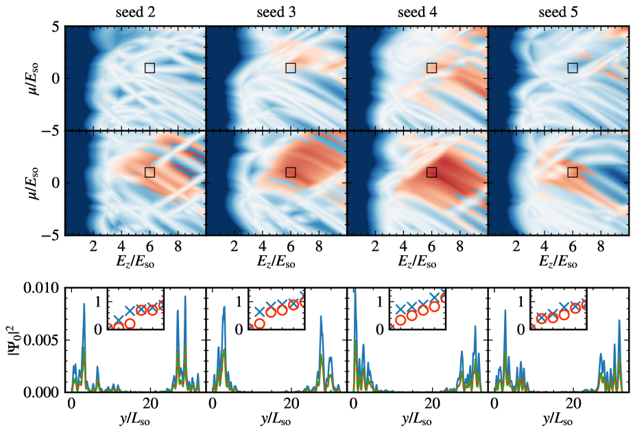
To demonstrate that the optimization reliably restores the topological phase, we consider several disorder realizations for onsite disorder with strength by using different seeds for the random number generator (seed 1 is used in the main text). In the top panel of Fig. 11, we show the topological gap for the disordered wires where all gate voltages are set to zero. At the point of optimization (black square), disorder destroyed the topological phase in four out of five cases (including the main text results), which is a realistic amount of disorder [22].
For a realistic test, we stop optimization after 3000 metric evaluations and use the best gate voltages at this point. In all cases, we find an extended topological phase (center panel) and localized MZMs (lower panel) when using the optimized gate voltages.
References
- Ladd et al. [2010] T. D. Ladd, F. Jelezko, R. Laflamme, Y. Nakamura, C. Monroe, and J. L. O’Brien, Quantum computers, Nature 464, 45 (2010).
- Kloeffel and Loss [2013] C. Kloeffel and D. Loss, Prospects for Spin-Based Quantum Computing in Quantum Dots, Annual Review of Condensed Matter Physics 4, 51 (2013).
- Vandersypen et al. [2017] L. M. K. Vandersypen, H. Bluhm, J. S. Clarke, A. S. Dzurak, R. Ishihara, A. Morello, D. J. Reilly, L. R. Schreiber, and M. Veldhorst, Interfacing spin qubits in quantum dots and donors—hot, dense, and coherent, npj Quantum Information 3, 34 (2017).
- Alicea et al. [2011] J. Alicea, Y. Oreg, G. Refael, F. von Oppen, and M. P. A. Fisher, Non-Abelian statistics and topological quantum information processing in 1D wire networks, Nature Physics 7, 412 (2011).
- Clarke et al. [2011] D. J. Clarke, J. D. Sau, and S. Tewari, Majorana fermion exchange in quasi-one-dimensional networks, Physical Review B 84, 035120 (2011).
- Hyart et al. [2013] T. Hyart, B. van Heck, I. C. Fulga, M. Burrello, A. R. Akhmerov, and C. W. J. Beenakker, Flux-controlled quantum computation with Majorana fermions, Physical Review B 88, 035121 (2013).
- Sarma et al. [2015] S. D. Sarma, M. Freedman, and C. Nayak, Majorana zero modes and topological quantum computation, npj Quantum Information 1, 15001 (2015).
- Aasen et al. [2016] D. Aasen, M. Hell, R. V. Mishmash, A. Higginbotham, J. Danon, M. Leijnse, T. S. Jespersen, J. A. Folk, C. M. Marcus, K. Flensberg, and J. Alicea, Milestones Toward Majorana-Based Quantum Computing, Physical Review X 6, 031016 (2016).
- Karzig et al. [2017] T. Karzig, C. Knapp, R. M. Lutchyn, P. Bonderson, M. B. Hastings, C. Nayak, J. Alicea, K. Flensberg, S. Plugge, Y. Oreg, C. M. Marcus, and M. H. Freedman, Scalable designs for quasiparticle-poisoning-protected topological quantum computation with Majorana zero modes, Physical Review B 95, 235305 (2017).
- Lutchyn et al. [2018] R. M. Lutchyn, Bakkers, E. P. A. M., L. P. Kouwenhoven, P. Krogstrup, C. M. Marcus, and Y. Oreg, Majorana zero modes in superconductor–semiconductor heterostructures, Nature Reviews Materials 3, 52 (2018).
- Oreg and von Oppen [2020] Y. Oreg and F. von Oppen, Majorana Zero Modes in Networks of Cooper-Pair Boxes: Topologically Ordered States and Topological Quantum Computation, Annual Review of Condensed Matter Physics 11, 397 (2020).
- Mandal et al. [2023] M. Mandal, N. C. Drucker, P. Siriviboon, T. Nguyen, T. Boonkird, T. N. Lamichhane, R. Okabe, A. Chotrattanapituk, and M. Li, Topological superconductors from a materials perspective, arXiv preprint arXiv:2303.15581 (2023).
- Vijay and Fu [2016] S. Vijay and L. Fu, Teleportation-based quantum information processing with Majorana zero modes, Physical Review B 94, 235446 (2016).
- Kitaev [2001] A. Y. Kitaev, Unpaired Majorana fermions in quantum wires, Physics-Uspekhi 44, 131 (2001).
- Lutchyn et al. [2010] R. M. Lutchyn, J. D. Sau, and S. Das Sarma, Majorana fermions and a topological phase transition in semiconductor-superconductor heterostructures, Physical review letters 105, 077001 (2010).
- Oreg et al. [2010] Y. Oreg, G. Refael, and F. von Oppen, Helical liquids and Majorana bound states in quantum wires, Physical review letters 105, 177002 (2010).
- Sau et al. [2010] J. D. Sau, S. Tewari, R. M. Lutchyn, T. D. Stanescu, and S. Das Sarma, Non-Abelian quantum order in spin-orbit-coupled semiconductors: Search for topological Majorana particles in solid-state systems, Physical Review B 82, 214509 (2010).
- Zhang et al. [2017] H. Zhang, Ö. Gül, S. Conesa-Boj, M. P. Nowak, M. Wimmer, K. Zuo, V. Mourik, F. K. de Vries, J. van Veen, M. W. A. de Moor, J. D. S. Bommer, D. J. van Woerkom, D. Car, S. R. Plissard, E. P. A. M. Bakkers, M. Quintero-Pérez, M. C. Cassidy, S. Koelling, S. Goswami, K. Watanabe, T. Taniguchi, and L. P. Kouwenhoven, Ballistic superconductivity in semiconductor nanowires, Nature Communications 8, 16025 (2017).
- Ahn et al. [2021] S. Ahn, H. Pan, B. Woods, T. D. Stanescu, and S. D. Sarma, Estimating disorder and its adverse effects in semiconductor Majorana nanowires, arXiv:2109.00007 (2021).
- Das Sarma and Pan [2021] S. Das Sarma and H. Pan, Disorder-induced zero-bias peaks in Majorana nanowires, Physical Review B 103, 195158 (2021).
- Yu et al. [2021] P. Yu, J. Chen, M. Gomanko, G. Badawy, Bakkers, E. P. A. M., K. Zuo, V. Mourik, and S. M. Frolov, Non-Majorana states yield nearly quantized conductance in proximatized nanowires, Nature Physics 17, 482 (2021).
- Aghaee et al. [2022] M. Aghaee, A. Akkala, Z. Alam, R. Ali, A. A. Ramirez, M. Andrzejczuk, A. E. Antipov, M. Astafev, B. Bauer, J. Becker, et al., Inas-al hybrid devices passing the topological gap protocol, arXiv preprint arXiv:2207.02472 (2022).
- Sarma et al. [2023] S. D. Sarma, J. D. Sau, and T. D. Stanescu, Spectral properties, topological patches, and effective phase diagrams of finite disordered majorana nanowires, arXiv preprint arXiv:2305.07007 (2023).
- Takei et al. [2013] S. Takei, B. M. Fregoso, H.-Y. Hui, A. M. Lobos, and S. Das Sarma, Soft superconducting gap in semiconductor Majorana nanowires, Physical review letters 110, 186803 (2013).
- Kells et al. [2012] G. Kells, D. Meidan, and P. W. Brouwer, Near-zero-energy end states in topologically trivial spin-orbit coupled superconducting nanowires with a smooth confinement, Physical Review B 86, 100503(R) (2012).
- Prada et al. [2012] E. Prada, P. San-Jose, and R. Aguado, Transport spectroscopy of n s nanowire junctions with majorana fermions, Physical Review B 86, 180503(R) (2012).
- Rainis et al. [2013] D. Rainis, L. Trifunovic, J. Klinovaja, and D. Loss, Towards a realistic transport modeling in a superconducting nanowire with Majorana fermions, Physical Review B 87, 024515 (2013).
- Cayao et al. [2015] J. Cayao, E. Prada, P. San-Jose, and R. Aguado, Sns junctions in nanowires with spin-orbit coupling: Role of confinement and helicity on the subgap spectrum, Physical Review B 91, 024514 (2015).
- San-Jose et al. [2016] P. San-Jose, J. Cayao, E. Prada, and R. Aguado, Majorana bound states from exceptional points in non-topological superconductors, Scientific reports 6, 21427 (2016).
- Chen et al. [2017] J. Chen, P. Yu, J. Stenger, M. Hocevar, D. Car, S. R. Plissard, E. P. A. M. Bakkers, T. D. Stanescu, and S. M. Frolov, Experimental phase diagram of zero-bias conductance peaks in superconductor/semiconductor nanowire devices, Science advances 3, e1701476 (2017).
- Liu et al. [2017] C.-X. Liu, J. D. Sau, T. D. Stanescu, and S. Das Sarma, Andreev bound states versus Majorana bound states in quantum dot-nanowire-superconductor hybrid structures: Trivial versus topological zero-bias conductance peaks, Physical Review B 96, 075161 (2017).
- Peñaranda et al. [2018] F. Peñaranda, R. Aguado, P. San-Jose, and E. Prada, Quantifying wave-function overlaps in inhomogeneous majorana nanowires, Physical Review B 98, 235406 (2018).
- Avila et al. [2019] J. Avila, F. Peñaranda, E. Prada, P. San-Jose, and R. Aguado, Non-hermitian topology as a unifying framework for the andreev versus majorana states controversy, Communications Physics 2, 133 (2019).
- Chiu and Das Sarma [2019] C.-K. Chiu and S. Das Sarma, Fractional Josephson effect with and without Majorana zero modes, Physical Review B 99, 035312 (2019).
- Chen et al. [2019] J. Chen, B. D. Woods, P. Yu, M. Hocevar, D. Car, S. R. Plissard, E. P. A. M. Bakkers, T. D. Stanescu, and S. M. Frolov, Ubiquitous Non-Majorana Zero-Bias Conductance Peaks in Nanowire Devices, Physical review letters 123, 107703 (2019).
- Woods et al. [2019] B. D. Woods, J. Chen, S. M. Frolov, and T. D. Stanescu, Zero-energy pinning of topologically trivial bound states in multiband semiconductor-superconductor nanowires, Physical Review B 100, 125407 (2019).
- Vuik et al. [2019] A. Vuik, B. Nijholt, A. Akhmerov, and M. Wimmer, Reproducing topological properties with quasi-Majorana states, SciPost Physics 7, 061 (2019).
- Awoga et al. [2019] O. A. Awoga, J. Cayao, and A. M. Black-Schaffer, Supercurrent detection of topologically trivial zero-energy states in nanowire junctions, Physical Review Letters 123, 117001 (2019).
- Dmytruk et al. [2020] O. Dmytruk, D. Loss, and J. Klinovaja, Pinning of andreev bound states to zero energy in two-dimensional superconductor-semiconductor rashba heterostructures, Physical Review B 102, 245431 (2020).
- Pan and Das Sarma [2020] H. Pan and S. Das Sarma, Physical mechanisms for zero-bias conductance peaks in Majorana nanowires, Physical Review Research 2, 013377 (2020).
- Prada et al. [2020] E. Prada, P. San-Jose, M. W. de Moor, A. Geresdi, E. J. Lee, J. Klinovaja, D. Loss, J. Nygård, R. Aguado, and L. P. Kouwenhoven, From Andreev to Majorana bound states in hybrid superconductor–semiconductor nanowires, Nature Reviews Physics 2, 575 (2020).
- Valentini et al. [2021] M. Valentini, F. Peñaranda, A. Hofmann, M. Brauns, R. Hauschild, P. Krogstrup, P. San-Jose, E. Prada, R. Aguado, and G. Katsaros, Nontopological zero-bias peaks in full-shell nanowires induced by flux-tunable andreev states, Science 373, 82 (2021).
- Zhang et al. [2021] H. Zhang, M. W. A. de Moor, J. D. S. Bommer, Di Xu, G. Wang, N. van Loo, C.-X. Liu, S. Gazibegovic, J. A. Logan, D. Car, Veld, Roy L. M. Op het, P. J. van Veldhoven, S. Koelling, M. A. Verheijen, M. Pendharkar, D. J. Pennachio, B. Shojaei, J. S. Lee, C. J. Palmstrøm, E. P. A. M. Bakkers, S. D. Sarma, and L. P. Kouwenhoven, Large zero-bias peaks in InSb-Al hybrid semiconductor-superconductor nanowire devices, arXiv preprint arXiv:2101.11456 (2021).
- Bagrets and Altland [2012] D. Bagrets and A. Altland, Class D spectral peak in Majorana quantum wires, Physical review letters 109, 227005 (2012).
- Pikulin et al. [2012] D. I. Pikulin, J. P. Dahlhaus, M. Wimmer, H. Schomerus, and C. W. J. Beenakker, A zero-voltage conductance peak from weak antilocalization in a Majorana nanowire, New Journal of Physics 14, 125011 (2012).
- Liu et al. [2012] J. Liu, A. C. Potter, K. T. Law, and P. A. Lee, Zero-bias peaks in the tunneling conductance of spin-orbit-coupled superconducting wires with and without Majorana end-states, Physical review letters 109, 267002 (2012).
- Whiticar et al. [2020] A. M. Whiticar, A. Fornieri, E. C. T. O’Farrell, A. C. C. Drachmann, T. Wang, C. Thomas, S. Gronin, R. Kallaher, G. C. Gardner, M. J. Manfra, C. M. Marcus, and F. Nichele, Coherent transport through a Majorana island in an Aharonov-Bohm interferometer, Nature Communications 11, 3212 (2020).
- Fu [2010] L. Fu, Electron teleportation via Majorana bound states in a mesoscopic superconductor, Physical review letters 104, 056402 (2010).
- Hell et al. [2018] M. Hell, K. Flensberg, and M. Leijnse, Distinguishing Majorana bound states from localized Andreev bound states by interferometry, Physical Review B 97, 161401(R) (2018).
- Thamm and Rosenow [2021] M. Thamm and B. Rosenow, Transmission amplitude through a Coulomb blockaded Majorana wire, Physical Review Research 3, 023221 (2021).
- Pikulin et al. [2021] D. I. Pikulin, B. van Heck, T. Karzig, E. A. Martinez, B. Nijholt, T. Laeven, G. W. Winkler, J. D. Watson, S. Heedt, M. Temurhan, et al., Protocol to identify a topological superconducting phase in a three-terminal device, arXiv preprint arXiv:2103.12217 (2021).
- Mourik et al. [2012] V. Mourik, K. Zuo, S. M. Frolov, S. R. Plissard, Bakkers, E. P. A. M., and L. P. Kouwenhoven, Signatures of Majorana fermions in hybrid superconductor-semiconductor nanowire devices, Science (New York, N.Y.) 336, 1003 (2012).
- Das et al. [2012] A. Das, Y. Ronen, Y. Most, Y. Oreg, M. Heiblum, and H. Shtrikman, Zero-bias peaks and splitting in an Al–InAs nanowire topological superconductor as a signature of Majorana fermions, Nature Physics 8, 887 (2012).
- Deng et al. [2012] M. T. Deng, C. L. Yu, G. Y. Huang, M. Larsson, P. Caroff, and H. Q. Xu, Anomalous zero-bias conductance peak in a Nb-InSb nanowire-Nb hybrid device, Nano Letters 12, 6414 (2012).
- Nichele et al. [2017] F. Nichele, A. C. C. Drachmann, A. M. Whiticar, E. C. T. O’Farrell, H. J. Suominen, A. Fornieri, T. Wang, G. C. Gardner, C. Thomas, A. T. Hatke, P. Krogstrup, M. J. Manfra, K. Flensberg, and C. M. Marcus, Scaling of Majorana Zero-Bias Conductance Peaks, Physical review letters 119, 136803 (2017).
- Rokhinson et al. [2012] L. P. Rokhinson, X. Liu, and J. K. Furdyna, The fractional a.c. Josephson effect in a semiconductor–superconductor nanowire as a signature of Majorana particles, Nature Physics 8, 795 (2012).
- Albrecht et al. [2016] S. M. Albrecht, A. P. Higginbotham, M. Madsen, F. Kuemmeth, T. S. Jespersen, J. Nygård, P. Krogstrup, and C. M. Marcus, Exponential protection of zero modes in Majorana islands, Nature 531, 206 (2016).
- Klinovaja et al. [2012] J. Klinovaja, P. Stano, and D. Loss, Transition from fractional to majorana fermions in rashba nanowires, Physical review letters 109, 236801 (2012).
- Boutin et al. [2018] S. Boutin, J. Camirand Lemyre, and I. Garate, Majorana bound state engineering via efficient real-space parameter optimization, Physical Review B 98, 214512 (2018).
- Mohanta et al. [2019] N. Mohanta, T. Zhou, J.-W. Xu, J. E. Han, A. D. Kent, J. Shabani, I. Žutić, and A. Matos-Abiague, Electrical Control of Majorana Bound States Using Magnetic Stripes, Physical Review Applied 12, 034048 (2019).
- Turcotte et al. [2020] S. Turcotte, S. Boutin, J. C. Lemyre, I. Garate, and M. Pioro-Ladrière, Optimized micromagnet geometries for Majorana zero modes in low g -factor materials, Physical Review B 102, 125425 (2020).
- Melo et al. [2022] A. Melo, T. Tanev, and A. R. Akhmerov, Greedy optimization of the geometry of majorana josephson junctions, arXiv preprint arXiv:2205.05689 (2022).
- Gül et al. [2015] Ö. Gül, D. J. Van Woerkom, I. van Weperen, D. Car, S. R. Plissard, E. P. Bakkers, and L. P. Kouwenhoven, Towards high mobility insb nanowire devices, Nanotechnology 26, 215202 (2015).
- Awoga et al. [2022a] O. A. Awoga, M. Leijnse, A. M. Black-Schaffer, and J. Cayao, Mitigating disorder-induced zero-energy states in weakly-coupled semiconductor-superconductor hybrid systems, arXiv preprint arXiv:2212.06061 (2022a).
- Awoga et al. [2022b] O. A. Awoga, J. Cayao, and A. M. Black-Schaffer, Robust topological superconductivity in weakly coupled nanowire-superconductor hybrid structures, Physical Review B 105, 144509 (2022b).
- Thamm and Rosenow [2023] M. Thamm and B. Rosenow, Machine learning optimization of majorana hybrid nanowires, Physical Review Letters 130, 116202 (2023).
- Hansen [2016] N. Hansen, The cma evolution strategy: A tutorial, arXiv preprint arXiv:1604.00772 (2016).
- Arute et al. [2019] F. Arute, K. Arya, R. Babbush, D. Bacon, J. C. Bardin, R. Barends, R. Biswas, S. Boixo, Brandao, Fernando G. S. L., D. A. Buell, B. Burkett, Y. Chen, Z. Chen, B. Chiaro, R. Collins, W. Courtney, A. Dunsworth, E. Farhi, B. Foxen, A. Fowler, C. Gidney, M. Giustina, R. Graff, K. Guerin, S. Habegger, M. P. Harrigan, M. J. Hartmann, A. Ho, M. Hoffmann, T. Huang, T. S. Humble, S. V. Isakov, E. Jeffrey, Z. Jiang, D. Kafri, K. Kechedzhi, J. Kelly, P. V. Klimov, S. Knysh, A. Korotkov, F. Kostritsa, D. Landhuis, M. Lindmark, E. Lucero, D. Lyakh, S. Mandrà, J. R. McClean, M. McEwen, A. Megrant, X. Mi, K. Michielsen, M. Mohseni, J. Mutus, O. Naaman, M. Neeley, C. Neill, M. Y. Niu, E. Ostby, A. Petukhov, J. C. Platt, C. Quintana, E. G. Rieffel, P. Roushan, N. C. Rubin, D. Sank, K. J. Satzinger, V. Smelyanskiy, K. J. Sung, M. D. Trevithick, A. Vainsencher, B. Villalonga, T. White, Z. J. Yao, P. Yeh, A. Zalcman, H. Neven, and J. M. Martinis, Quantum supremacy using a programmable superconducting processor, Nature 574, 505 (2019).
- Lennon et al. [2019] D. T. Lennon, H. Moon, L. C. Camenzind, L. Yu, D. M. Zumbühl, G. A. D. Briggs, M. A. Osborne, E. A. Laird, and N. Ares, Efficiently measuring a quantum device using machine learning, npj Quantum Information 5, 79 (2019).
- Ares [2021] N. Ares, Machine learning as an enabler of qubit scalability, Nature Reviews Materials 6, 870 (2021).
- Baart et al. [2016] T. A. Baart, P. T. Eendebak, C. Reichl, W. Wegscheider, and L. M. K. Vandersypen, Computer-automated tuning of semiconductor double quantum dots into the single-electron regime, Applied Physics Letters 108, 213104 (2016).
- Botzem et al. [2018] T. Botzem, M. D. Shulman, S. Foletti, S. P. Harvey, O. E. Dial, P. Bethke, P. Cerfontaine, R. P. G. McNeil, D. Mahalu, V. Umansky, A. Ludwig, A. Wieck, D. Schuh, D. Bougeard, A. Yacoby, and H. Bluhm, Tuning Methods for Semiconductor Spin Qubits, Physical Review Applied 10, 054026 (2018).
- Kalantre et al. [2019] S. S. Kalantre, J. P. Zwolak, S. Ragole, X. Wu, N. M. Zimmerman, M. D. Stewart, and J. M. Taylor, Machine learning techniques for state recognition and auto-tuning in quantum dots, npj Quantum Information 5, 6 (2019).
- Teske et al. [2019] J. D. Teske, S. S. Humpohl, R. Otten, P. Bethke, P. Cerfontaine, J. Dedden, A. Ludwig, A. D. Wieck, and H. Bluhm, A machine learning approach for automated fine-tuning of semiconductor spin qubits, Applied Physics Letters 114, 133102 (2019).
- Mills et al. [2019] A. R. Mills, M. M. Feldman, C. Monical, P. J. Lewis, K. W. Larson, A. M. Mounce, and J. R. Petta, Computer-automated tuning procedures for semiconductor quantum dot arrays, Applied Physics Letters 115, 113501 (2019).
- Durrer et al. [2020] R. Durrer, B. Kratochwil, J. V. Koski, A. J. Landig, C. Reichl, W. Wegscheider, T. Ihn, and E. Greplova, Automated Tuning of Double Quantum Dots into Specific Charge States Using Neural Networks, Physical Review Applied 13, 054019 (2020).
- Moon et al. [2020] H. Moon, D. T. Lennon, J. Kirkpatrick, N. M. van Esbroeck, L. C. Camenzind, L. Yu, F. Vigneau, D. M. Zumbühl, G. A. D. Briggs, M. A. Osborne, D. Sejdinovic, E. A. Laird, and N. Ares, Machine learning enables completely automatic tuning of a quantum device faster than human experts, Nature Communications 11, 4161 (2020).
- van Esbroeck et al. [2020] N. M. van Esbroeck, D. T. Lennon, H. Moon, V. Nguyen, F. Vigneau, L. C. Camenzind, L. Yu, D. M. Zumbühl, G. A. D. Briggs, D. Sejdinovic, and N. Ares, Quantum device fine-tuning using unsupervised embedding learning, New Journal of Physics 22, 095003 (2020).
- [79] D. L. Craig, H. Moon, F. Fedele, D. T. Lennon, B. van Straaten, F. Vigneau, L. C. Camenzind, D. M. Zumbühl, G. A. D. Briggs, M. A. Osborne, D. Sejdinovic, and N. Ares, Bridging the reality gap in quantum devices with physics-aware machine learning.
- Fedele et al. [2021] F. Fedele, A. Chatterjee, S. Fallahi, G. C. Gardner, M. J. Manfra, and F. Kuemmeth, Simultaneous Operations in a Two-Dimensional Array of Singlet-Triplet Qubits, PRX Quantum 2, 040306 (2021).
- [81] J. Ziegler, T. McJunkin, E. S. Joseph, S. S. Kalantre, B. Harpt, D. E. Savage, M. G. Lagally, M. A. Eriksson, J. M. Taylor, and J. P. Zwolak, Toward Robust Autotuning of Noisy Quantum Dot Devices.
- Krause et al. [2022] O. Krause, A. Chatterjee, F. Kuemmeth, and E. van Nieuwenburg, Learning coulomb diamonds in large quantum dot arrays, arXiv preprint arXiv:2205.01443 (2022).
- Frees et al. [2019] A. Frees, J. K. Gamble, D. R. Ward, R. Blume-Kohout, M. A. Eriksson, M. Friesen, and S. N. Coppersmith, Compressed Optimization of Device Architectures for Semiconductor Quantum Devices, Physical Review Applied 11, 024063 (2019).
- Ruiz Euler et al. [2020] H.-C. Ruiz Euler, M. N. Boon, J. T. Wildeboer, B. van de Ven, T. Chen, H. Broersma, P. A. Bobbert, and W. G. van der Wiel, A deep-learning approach to realizing functionality in nanoelectronic devices, Nature Nanotechnology 15, 992 (2020).
- Danon et al. [2020] J. Danon, A. B. Hellenes, E. B. Hansen, L. Casparis, A. P. Higginbotham, and K. Flensberg, Nonlocal conductance spectroscopy of andreev bound states: Symmetry relations and bcs charges, Physical Review Letters 124, 036801 (2020).
- Akhmerov et al. [2011] A. Akhmerov, J. Dahlhaus, F. Hassler, M. Wimmer, and C. Beenakker, Quantized conductance at the majorana phase transition in a disordered superconducting wire, Physical review letters 106, 057001 (2011).
- Hansen [2006] N. Hansen, The CMA Evolution Strategy: A Comparing Review, in Towards a New Evolutionary Computation, Studies in Fuzziness and Soft Computing, edited by J. A. Lozano, E. Bengoetxea, I. Inza, and P. Larrañaga (Springer-Verlag Berlin Heidelberg, Berlin, Heidelberg, 2006) pp. 75–102.
- Lozano et al. [2006] J. A. Lozano, E. Bengoetxea, I. Inza, and P. Larrañaga, eds., Towards a New Evolutionary Computation: Advances in the Estimation of Distribution Algorithms, Studies in Fuzziness and Soft Computing, Vol. 192 (Springer-Verlag Berlin Heidelberg, Berlin, Heidelberg, 2006).
- Loshchilov and Hutter [2016] I. Loshchilov and F. Hutter, CMA-ES for Hyperparameter Optimization of Deep Neural Networks, arxiv:1604.07269 (2016).
- Willjuice Iruthayarajan and Baskar [2010] M. Willjuice Iruthayarajan and S. Baskar, Covariance matrix adaptation evolution strategy based design of centralized PID controller, Expert Systems with Applications 37, 5775 (2010).
- Loshchilov et al. [2013] I. Loshchilov, M. Schoenauer, and M. Sebag, Bi-population cma-es agorithms with surrogate models and line searches, in Proceedings of the 15th annual conference companion on Genetic and evolutionary computation (2013) pp. 1177–1184.
- Groth et al. [2014] C. W. Groth, M. Wimmer, A. R. Akhmerov, and X. Waintal, Kwant: a software package for quantum transport, New Journal of Physics 16, 063065 (2014).
- Winkler et al. [2019] G. W. Winkler, A. E. Antipov, B. Van Heck, A. A. Soluyanov, L. I. Glazman, M. Wimmer, and R. M. Lutchyn, Unified numerical approach to topological semiconductor-superconductor heterostructures, Physical Review B 99, 245408 (2019).
- Pöschl [2022] A. Pöschl, Nonlocal transport signatures of Andreev Bound States, PhD thesis, Center for Quantum Devices, Niels Bohr Institute, University of Copenhagen (2022).
- Cayao and Burset [2021] J. Cayao and P. Burset, Confinement-induced zero-bias peaks in conventional superconductor hybrids, Physical Review B 104, 134507 (2021).
- Nikolaus Hansen et al. [2021] Nikolaus Hansen, yoshihikoueno, ARF1, Kento Nozawa, Matthew Chan, Youhei Akimoto, and Dimo Brockhoff, CMA-ES/pycma: r3.1.0 (Zenodo, 2021).