These authors contributed equally to this work. \equalcontThese authors contributed equally to this work. [4]Ben J. Powell [2,5]Nikhil V. Medhekar [1,2]Agustin Schiffrin 1]School of Physics and Astronomy, Monash University, Clayton, Victoria 3800, Australia 2]ARC Centre of Excellence in Future Low-Energy Electronics Technologies, Monash University, Clayton, Victoria 3800, Australia 3]Quantum Information Science and Technology Unit, Okinawa Institute of Science and Technology Graduate University, Onna-son, Okinawa 904-0495, Japan 4]School of Mathematics and Physics, The University of Queensland, Brisbane, Queensland 4072, Australia 5]Department of Materials Science and Engineering, Monash University, Clayton, Victoria 3800, Australia
Gate control of Mott metal-insulator transition in a 2D metal-organic framework
Abstract
Strong electron-electron Coulomb interactions in materials can lead to a vast range of exotic many-body quantum phenomena, including Mott metal-insulator transitions, magnetic order, quantum spin liquids, and unconventional superconductivity. These many-body phases are strongly dependent on band occupation and can hence be controlled via the chemical potential. Flat electronic bands in two-dimensional (2D) and layered materials such as the kagome lattice, enhance strong electronic correlations. Although theoretically predicted, correlated-electron phases in monolayer 2D metal-organic frameworks (MOFs) – which benefit from efficient synthesis protocols and tunable properties – with a kagome structure have not yet been realised experimentally. Here, we synthesise a 2D kagome MOF comprised of 9,10-dicyanoanthracene molecules and copper atoms on an atomically thin insulator, monolayer hexagonal boron nitride (hBN) on Cu(111). Scanning tunnelling microscopy (STM) and spectroscopy reveal an electronic energy gap of 200 meV in this MOF, consistent with dynamical mean-field theory predictions of a Mott insulating phase. By tuning the electron population of kagome bands, via either template-induced (via local work function variations of the hBN/Cu(111) substrate) or tip-induced (via the STM probe) gating, we are able to induce Mott metal-insulator transitions in the MOF. These findings pave the way for devices and technologies based on 2D MOFs and on electrostatic control of many-body quantum phases therein.
keywords:
Strongly correlated electrons, metal-organic frameworks, kagome, dynamical mean-field theory, scanning probe microscopy, Mott insulator, metal-insulator transitionStrong electronic correlations arise in a material at specific electron fillings of its bands, provided that the on-site Coulomb repulsion (characterised by the Hubbard energy, ) is of the order of or larger than the bandwidth, . These electronic correlations can result in a wide range of exotic many-body quantum phases. Examples include correlated insulating phases, quantum spin liquids (QSL), correlated magnetism, and superconductivity – phenomena which have been realised in monolayer transition metal-dichalcogenides nakata_monolayer_2016 ; liu_monolayer_2021 ; lin_scanning_2020 ; chen_strong_2020 ; ruan_evidence_2021 ; chen_evidence_2022 , twisted few-layer graphene cao_unconventional_2018 ; park_tunable_2021 , inorganic kagome crystals zheng_emergent_2022 ; ye_massive_2018 ; yin_quantum-limit_2020 , and organic charge transfer salts powell_quantum_2011 ; kanoda_mott_2011 ; miksch_gapped_2021 .
Tuning of the chemical potential via electrostatic gating can allow for control over such band electron filling, enabling reversible switching between correlated phases cao_unconventional_2018 . This makes these systems amenable to integration as active materials in voltage-controlled devices, offering enticing prospects for applications in electronics, spintronics, and information processing and storage powell_quantum_2011 ; shao_recent_2018 .
Two-dimensional (2D) materials have emerged as particularly promising candidates for realising strongly correlated phenomena as the absence of interlayer hopping and screening can contribute to decreasing and increasing chen_strong_2020 . Additionally, some 2D crystal geometries – such as the kagome structure – give rise to intrinsic flat electronic bands balents_superconductivity_2020 ; neupert_charge_2022 . When these bands of extremely narrow are half-filled, even weak Coulomb repulsion can open an energy gap and give rise to a Mott insulating phase powell_quantum_2011 . Away from half-filling, the gap closes and the system becomes metallic.
Metal-organic frameworks (MOFs) are a broad class of materials whose properties are highly tunable through careful selection of constituent organic molecules and metal atoms cui_metalorganic_2016 . There has been growing interest in 2D MOFs for their electronic zhang_intrinsic_2016 ; jin_large-gap_2018 ; jiang_exotic_2021 and magnetic properties yamada_designing_2017 ; zhang_two-dimensional_2019 , including strongly correlated phases fuchs_kagome_2020 ; takenaka_strongly_2021 ; kumar_manifestation_2021 ; nourse_multiple_2021 .
Here, we demonstrate electrostatic control over a Mott metal-insulator-transition (MIT) in a single-layer 2D kagome MOF, in excellent agreement with theoretical predictions.
1 Results and Discussion
1.1 A 2D metal-organic framework on an atomically thin insulator
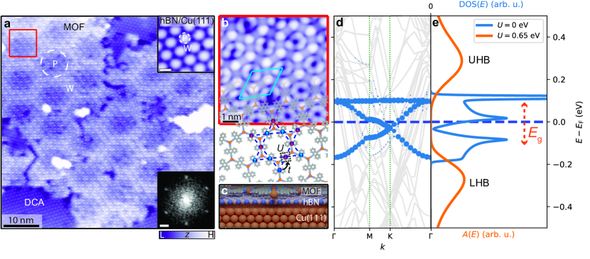
We synthesised the MOF – consisting of 9,10-dicyanoanthracene (DCA) molecules coordinated to copper (Cu) atoms – on monolayer hexagonal boron nitride (hBN) on Cu(111) (see Methods for sample preparation). A scanning tunnelling microscopy (STM) image of a crystalline MOF domain grown seamlessly across the hBN/Cu(111) substrate is shown in Fig. 1a. The long-range modulation of the MOF STM apparent height follows the hBN/Cu(111) moiré pattern, which arises due to mismatch between the hBN and Cu(111) lattices (giving rise to ‘pore’, P, and ‘wire’, W, regions – see upper inset) joshi_boron_2012 ; zhang_tuning_2018 ; auwarter_hexagonal_2019 .
The MOF is characterised by a hexagonal lattice (lattice constant: 2.01 0.06 nm), with a unit cell including two Cu atoms (honeycomb arrangement; bright protrusions in Fig. 1b) and three DCA molecules (kagome arrangement, with protrusions at both ends of anthracene backbone in Fig. 1b), similar to previous reports yan_synthesis_2021 ; yan_two-dimensional_2021 ; kumar_manifestation_2021 ; hernandez-lopez_searching_2021 .
We calculated the bandstructure of this DCA3Cu2 MOF on hBN/Cu(111) by density functional theory (DFT; with ); Fig. 1d. Projection of the Kohn-Sham wavefunctions onto MOF states shows the prototypical kagome energy dispersion with two Dirac bands and a flat band, consistent with prior theoretical calculations for the freestanding MOF zhang_intrinsic_2016 ; fuchs_kagome_2020 ; field_correlation-induced_2022 . This near-Fermi bandstructure has predominantly molecular DCA character, and is well described by a nearest-neighbour tight-binding (TB) model (see corresponding density of electronic states, DOS, as a function of energy in Fig. 1e field_correlation-induced_2022 ). The hBN monolayer, a 2D insulator with a bandgap eV auwarter_hexagonal_2019 , prevents electronic hybridization between the underlying Cu(111) surface and the 2D MOF auwarter_hexagonal_2019 . This allows the MOF to preserve its intrinsic electronic properties, in contrast to previous findings on metal surfaces pawin_surface_2008 ; hernandez-lopez_searching_2021 ; kumar_manifestation_2021 ; field_correlation-induced_2022 . These calculations predict that the MOF on hBN/Cu(111) is metallic, with some electron transfer from substrate to MOF leading to the chemical potential lying above the Dirac (charge neutrality) point, close to half-filling of the three kagome bands (Fig. 1d).
Strong electronic interactions have been theoretically predicted in DCA3Cu2 fuchs_kagome_2020 , and a signature was recently detected experimentally kumar_manifestation_2021 . We therefore calculated the many-body spectral function – analogous to the DOS in the non-interacting regime – of the free-standing MOF via dynamical mean-field theory (DMFT). In contrast to the TB model or DFT, DMFT explicitly captures electronic correlations caused by the Hubbard energy (see Methods) georges_dynamical_1996 . Fig. 1e shows for = 0.65 eV (consistent with previous experimental estimates yan_synthesis_2021 ) and for a chemical potential which matches the DFT-predicted occupation of the kagome bands for the MOF on hBN/Cu(111) (see Fig. S1 for further DMFT calculations). We observe two broad peaks (lower and upper Hubbard bands) separated by an energy gap of 200 meV, dramatically different from the non-interacting kagome DOS, and indicative of a Mott insulating phase ohashi_mott_2006 ; fuchs_kagome_2020 .
1.2 Observation of 200 meV Mott energy gap
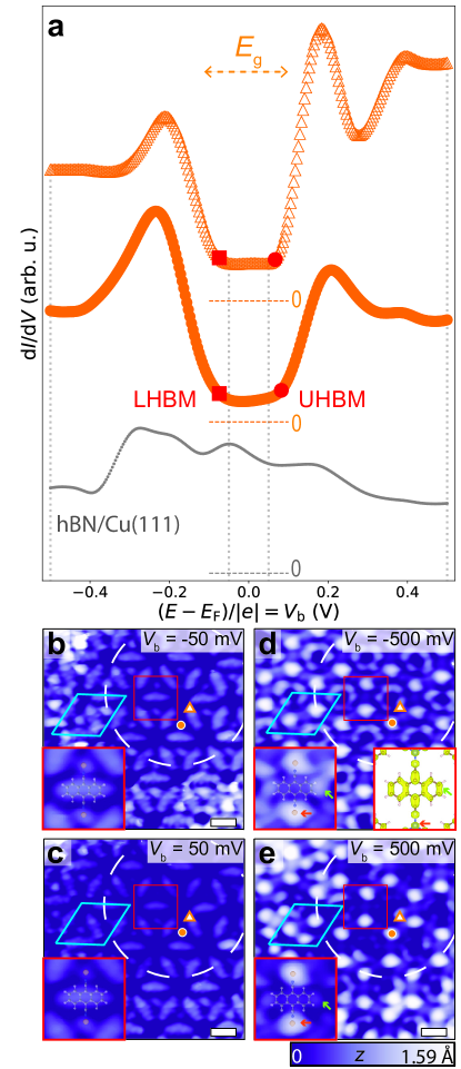
To experimentally probe the electronic properties of DCA3Cu2/hBN/Cu(111), we conducted differential conductance () scanning tunnelling spectroscopy (STS); is an approximation of the local DOS () in the non-interacting (interacting, respectively) picture. We performed STS at the ends of the DCA anthracene moiety and at the Cu sites of the MOF – locations where we expect the strongest signature of the kagome bands based on the spatial distribution of the orbitals that give rise to these bands yan_synthesis_2021 ; yan_two-dimensional_2021 ; kumar_manifestation_2021 . These spectra (Fig. 2a), taken at a pore region of the hBN/Cu(111) moiré pattern, both show broad peaks at bias voltages and 0.2 V. In a bias voltage window of 0.2 V around the chemical potential (), the signal is low, significantly smaller than that for bare hBN/Cu(111).
STM images acquired within this low- bias voltage window (Fig. 2b, c) show mainly the topography of the MOF, with the molecules appearing as ellipses and the Cu atoms as protrusions, with uniform intensity. Outside the low- bias voltage window ( mV), Cu sites and the ends of the DCA anthracene moieties appear as bright protrusions (Fig. 2d, e), similar to the spatial distribution of the electronic orbitals of the DCA3Cu2 MOF associated with the near-Fermi kagome bands (right inset of Fig. 2d; see Figs. S7-S8 for more -dependent STM images and maps) yan_synthesis_2021 ; yan_two-dimensional_2021 ; kumar_manifestation_2021 .
This suggests that the peaks at V in Fig. 2a are related to intrinsic MOF electronic states near , with the low- bias voltage window of 0.2 V around representing an energy gap, , between these states. This is consistent with in-gap topographic STM imaging in Fig. 2b, c repp_molecules_2005 . These peaks cannot be attributed to inelastic tunnelling (e.g., MOF vibrational modes) as they are not always symmetric about (see Fig. 3). The gap is much larger than that predicted from spin-orbit coupling in such a system zhang_intrinsic_2016 , and the highly crystalline growth (Fig. 1a) makes a large disorder-related gap unlikely. Furthermore, the gap is inconsistent with DFT and TB calculations (Fig. 1d, e).
1.3 Template-induced Mott metal-insulator transition
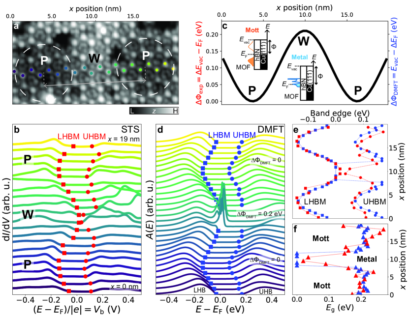
We further measured spectra of the DCA3Cu2 MOF across the hBN/Cu(111) moiré pattern (Fig. 3a, b). In Fig. 3e-f, is centred symmetrically about for spectra taken in the middle of a pore region, while those taken closer to the wire region show the gap shifting upwards in energy (lowering the barrier to creation of a hole). We then observe drastically collapse to zero at the centre of the wire region.
The hBN/Cu(111) moiré pattern consists of a modulation of the local work function (with little structural corrugation), where the quantity depends on the period of the moiré superstructure, joshi_boron_2012 ; zhang_tuning_2018 ; auwarter_hexagonal_2019 . For nm, as for the hBN/Cu(111) domain in Fig. 3a, eV (Fig. 3c) zhang_tuning_2018 . Due to energy level alignment joshi_control_2014 ; zimmermann_self-assembly_2020 ; portner_charge_2020 , this corrugation of affects substrate-to-MOF electron transfer and hence the effective electron filling of the MOF bands, with this filling smaller at wire than pore regions joshi_control_2014 ; kumar_mesoscopic_2023 . This is consistent with the effective reduction of the hole creation barrier at the wire relative to the pore in Fig. 3b.
To capture the effect of this moiré-induced modulation of on the MOF electronic properties, we conducted further DMFT calculations. Using 0.65 eV (the same as Fig. 1e), we calculated for a range of assuming a uniform system (neglecting the experimental spatial variation of ). We considered a sinusoidal variation of , with an amplitude of 0.2 eV, to match the experimental for this specific hBN/Cu(111) moiré domain kumar_mesoscopic_2023 ; zhang_tuning_2018 (Fig. 3c; see Methods). The obtained (Fig. 3d) quantitatively reproduce the experimental spectra in Fig. 3b, including the LHBM and UHBM (Fig. 3e), and the collapse of at the wire region (Fig. 3f). This provides compelling evidence that our DMFT calculations capture the fundamental electronic properties of the 2D DCA3Cu2 MOF, hosting Mott insulating ( meV) and metal-like phases () controllable via electron filling of the MOF.
The DMFT-calculated spectral functions for the ungapped metal-like phase (for the smallest electron filling corresponding to measurements at the wire region; Fig. 3c) show peaks near (Fig. 3d) which were not observed experimentally. These peaks are indicative of coherent quasiparticles georges_dynamical_1996 , with their width associated with the quasiparticle lifetime and quasiparticle mean free path . Via our DMFT and TB calculations (supplementary section S2), we estimate nm, much larger than the wire region width of 4 nm. We hypothesize that the coherence peaks are suppressed in the experiment as quasiparticles are strongly scattered by the pore regions (where the MOF remains insulating).
1.4 Tip-induced Mott metal-insulator transition
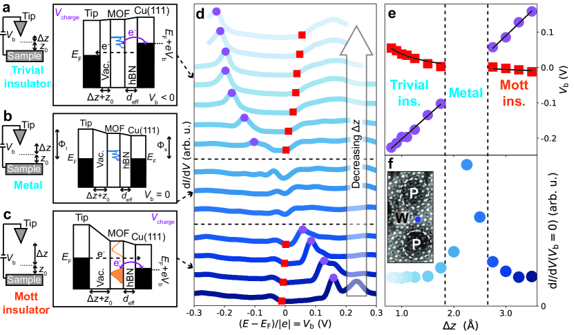
We also performed STS of the MOF as a function of tip-sample distance (where is set by tunnelling parameters), at the centre of a wire region (Fig. 4d; see Fig. S13 for pore). The spectra feature a peak (purple circles in Fig. 4d; sharper than band features in Fig. 3b) whose energy position increases linearly (Fig. 4e) with increasing . Conversely, the energy position of a subtler band edge (red squares) decreases with increasing , non-linearly and at a lower rate (Fig. 4e). These features cross the Fermi level for the same intermediate , as the spectrum becomes gapless ().
As is applied between the tip and Cu substrate, the STM double-barrier tunnel junction (DBTJ) – where the vacuum between tip and MOF is a first tunnel barrier and the insulating hBN is a second one – results in a voltage drop at the MOF location. This can lead to energy shifts of MOF states and/or charging of such states when they become resonant with the Cu(111) Fermi level (Fig. 4a) kumar_electric_2019 ; portner_charge_2020 ; yan_synthesis_2021 . In this scenario, the bias voltages corresponding to an intrinsic electronic state, , and to charging of such a state, , vary as a function of as:
| (1) |
| (2) |
where is the effective width of the hBN tunnel barrier, is the bias voltage corresponding to the electronic state as , and is the difference between tip and sample work functions kumar_electric_2019 .
We fit the -dependent bias voltage associated with the subtle band edge (red squares) in Fig. 4d with Eq. (1), and the bias voltage associated with the sharp peak (purple circles) with Eq. (2) (Fig. 4e). The agreement between experimental data and fits indicate that the subtle spectral band edge (red) represents an intrinsic MOF electronic state, with its energy shifting as varies, and with the sharp peak (purple) corresponding to charging of such a state.
We interpret these results as follows. At the wire site, for large (Fig. 4c), the MOF electronic states are strongly pinned to the substrate, and the MOF near-Fermi kagome bands are approximately half-filled. Here, the MOF is in a Mott insulating phase with a correlated energy gap (bottom spectra of Fig. 4d), with the top of the lower Hubbard band susceptible to charging (as becomes more positive). As decreases gradually to intermediate values (Fig. 4b), the MOF states become less pinned to the substrate, and the difference between tip () and local sample () work functions (with ; see supplementary section S10) leads to an electron filling of the near-Fermi MOF bands smaller than half-filling. Here, the Mott energy gap collapses and the MOF is in a metallic phase, as shown by the increase in Fermi level signal (for ; Fig. 4f and Figs. S1, S14). As further diminishes (Fig. 4a), the near-Fermi MOF states become more pinned to the tip and depopulate, becoming susceptible to charging (as becomes more negative). Here, the MOF is a trivial insulator (top spectra of Fig. 4d). The STM tip, via and , acts as an electrostatic gate that switches the 2D MOF from Mott insulator to metal to trivial insulator (Fig. S12).
The electrostatic effect of the tip at the wire region is highly localised. Whether the injected holes are truly delocalised in an extended metallic phase remains an open question, requiring further investigations (e.g., transport experiments).
The spectra for large in Fig. 4d – when the influence of the tip on the system is minimised – suggest that, even at the wire region, the MOF is intrinsically in a Mott insulating phase, unlike what is shown in Fig. 3. In the latter, the MOF is in an gapless phase at the wire site, as is below half-filling due to the combination of a large (in comparison with ) and an intermediate (supplementary section S3).
2 Conclusion
We have demonstrated that single-layer DCA3Cu2 not only hosts a robust Mott insulating phase (with at K), but also that Mott MITs can be achieved via template- (Fig. 3) and tip- (Fig. 4) induced gating, quantitatively consistent with DMFT and the DBTJ model. This shows that such phase transitions can be controlled via electrostatic tuning of the chemical potential.
Monolayer DCA3Cu2 has been studied on other substrates pawin_surface_2008 ; yan_synthesis_2021 ; yan_two-dimensional_2021 ; hernandez-lopez_searching_2021 ; kumar_manifestation_2021 , without observing a Mott phase. In our case, the combination of the wide bandgap hBN as a template (allowing the MOF to retain its intrinsic electronic properties), and of the adequate energy level alignment given by the hBN/Cu(111) substrate (resulting in half-filling of kagome bands; Fig. 1d), plays a key role in the realisation of the correlated-electron Mott phase.
Our findings represent a promising step toward incorporation of 2D MOFs as active materials in device-like architectures (e.g., van der Waals heterostructures based on 2D materials), benefiting from efficient synthesis approaches and versatility offered by MOFs, and allowing for access and control of correlated-electron phases therein via electrostatic gating riss_imaging_2014 . Our work establishes single-layer 2D MOFs – with crystal geometries allowing for flat bands – as promising platforms for controllable switching between diverse many-body quantum phenomena, potentially including correlated magnetism, superconductivity, and QSLs.
References
- \bibcommenthead
- (1) Nakata, Y. et al. Monolayer 1T-NbSe2 as a Mott insulator. NPG Asia Mater 8 (11), e321–e321 (2016) .
- (2) Liu, M. et al. Monolayer 1T-NbSe2 as a 2D-correlated magnetic insulator. Science Advances 7 (47), eabi6339 (2021) .
- (3) Lin, H. et al. Scanning tunneling spectroscopic study of monolayer 1T-TaS2 and 1T-TaSe2. Nano Res. 13 (1), 133–137 (2020) .
- (4) Chen, Y. et al. Strong correlations and orbital texture in single-layer 1T-TaSe2. Nat. Phys. 16 (2), 218–224 (2020) .
- (5) Ruan, W. et al. Evidence for quantum spin liquid behaviour in single-layer 1T-TaSe2 from scanning tunnelling microscopy. Nat. Phys. 17 (10), 1154–1161 (2021) .
- (6) Chen, Y. et al. Evidence for a spinon Kondo effect in cobalt atoms on single-layer 1T-TaSe2. Nat. Phys. 18 (11), 1335–1340 (2022) .
- (7) Cao, Y. et al. Unconventional superconductivity in magic-angle graphene superlattices. Nature 556 (7699), 43–50 (2018) .
- (8) Park, J. M., Cao, Y., Watanabe, K., Taniguchi, T. & Jarillo-Herrero, P. Tunable strongly coupled superconductivity in magic-angle twisted trilayer graphene. Nature 590 (7845), 249–255 (2021) .
- (9) Zheng, L. et al. Emergent charge order in pressurized kagome superconductor CsV3Sb5. Nature 611 (7937), 682–687 (2022) .
- (10) Ye, L. et al. Massive Dirac fermions in a ferromagnetic kagome metal. Nature 555 (7698), 638–642 (2018) .
- (11) Yin, J.-X. et al. Quantum-limit Chern topological magnetism in TbMn6Sn6. Nature 583 (7817), 533–536 (2020) .
- (12) Powell, B. J. & McKenzie, R. H. Quantum frustration in organic Mott insulators: from spin liquids to unconventional superconductors. Rep. Prog. Phys. 74 (5), 056501 (2011) .
- (13) Kanoda, K. & Kato, R. Mott Physics in Organic Conductors with Triangular Lattices. Annual Review of Condensed Matter Physics 2 (1), 167–188 (2011) .
- (14) Miksch, B. et al. Gapped magnetic ground state in quantum spin liquid candidate k-(BEDT-TTF)2Cu2(CN)3. Science 372 (6539), 276–279 (2021) .
- (15) Shao, Z., Cao, X., Luo, H. & Jin, P. Recent progress in the phase-transition mechanism and modulation of vanadium dioxide materials. NPG Asia Mater 10 (7), 581–605 (2018) .
- (16) Balents, L., Dean, C. R., Efetov, D. K. & Young, A. F. Superconductivity and strong correlations in moiré flat bands. Nat. Phys. 16 (7), 725–733 (2020) .
- (17) Neupert, T., Denner, M. M., Yin, J.-X., Thomale, R. & Hasan, M. Z. Charge order and superconductivity in kagome materials. Nat. Phys. 18 (2), 137–143 (2022) .
- (18) Cui, Y. et al. Metal–Organic Frameworks as Platforms for Functional Materials. Acc. Chem. Res. 49 (3), 483–493 (2016) .
- (19) Zhang, L. Z. et al. Intrinsic Two-Dimensional Organic Topological Insulators in Metal–Dicyanoanthracene Lattices. Nano Lett. 16 (3), 2072–2075 (2016) .
- (20) Jin, Y. et al. Large-gap quantum anomalous Hall phase in hexagonal organometallic frameworks. Phys. Rev. B 98 (24), 245127 (2018) .
- (21) Jiang, W., Ni, X. & Liu, F. Exotic Topological Bands and Quantum States in Metal–Organic and Covalent–Organic Frameworks. Acc. Chem. Res. 54 (2), 416–426 (2021) .
- (22) Yamada, M. G., Fujita, H. & Oshikawa, M. Designing Kitaev Spin Liquids in Metal-Organic Frameworks. Phys. Rev. Lett. 119 (5), 057202 (2017) .
- (23) Zhang, L.-C. et al. Two-dimensional magnetic metal–organic frameworks with the Shastry-Sutherland lattice. Chem. Sci. 10 (44), 10381–10387 (2019) .
- (24) Fuchs, M. et al. Kagome metal-organic frameworks as a platform for strongly correlated electrons. J. Phys. Mater. 3 (2), 025001 (2020) .
- (25) Takenaka, T. et al. Strongly correlated superconductivity in a copper-based metal-organic framework with a perfect kagome lattice. Science Advances 7 (12), eabf3996 (2021) .
- (26) Kumar, D. et al. Manifestation of Strongly Correlated Electrons in a 2D Kagome Metal–Organic Framework. Advanced Functional Materials 31 (48), 2106474 (2021) .
- (27) Nourse, H. L., McKenzie, R. H. & Powell, B. J. Multiple insulating states due to the interplay of strong correlations and lattice geometry in a single-orbital Hubbard model. Phys. Rev. B 103 (8), L081114 (2021) .
- (28) Joshi, S. et al. Boron Nitride on Cu(111): An Electronically Corrugated Monolayer. Nano Lett. 12 (11), 5821–5828 (2012) .
- (29) Zhang, Q. et al. Tuning Band Gap and Work Function Modulations in Monolayer hBN/Cu(111) Heterostructures with Moiré Patterns. ACS Nano 12 (9), 9355–9362 (2018) .
- (30) Auwärter, W. Hexagonal boron nitride monolayers on metal supports: Versatile templates for atoms, molecules and nanostructures. Surface Science Reports 74 (1), 1–95 (2019) .
- (31) Yan, L. et al. Synthesis and Local Probe Gating of a Monolayer Metal-Organic Framework. Advanced Functional Materials 31 (22), 2100519 (2021) .
- (32) Yan, L. et al. Two-Dimensional Metal–Organic Framework on Superconducting NbSe2. ACS Nano 15 (11), 17813–17819 (2021) .
- (33) Hernández-López, L. et al. Searching for kagome multi-bands and edge states in a predicted organic topological insulator. Nanoscale 13 (10), 5216–5223 (2021) .
- (34) Field, B., Schiffrin, A. & Medhekar, N. V. Correlation-induced magnetism in substrate-supported 2D metal-organic frameworks. npj Comput Mater 8 (1), 1–10 (2022) .
- (35) Pawin, G. et al. A Surface Coordination Network Based on Substrate-Derived Metal Adatoms with Local Charge Excess. Angewandte Chemie International Edition 47 (44), 8442–8445 (2008) .
- (36) Georges, A., Kotliar, G., Krauth, W. & Rozenberg, M. J. Dynamical mean-field theory of strongly correlated fermion systems and the limit of infinite dimensions. Rev. Mod. Phys. 68 (1), 13–125 (1996) .
- (37) Ohashi, T., Kawakami, N. & Tsunetsugu, H. Mott Transition in Kagome Lattice Hubbard Model. Phys. Rev. Lett. 97 (6), 066401 (2006) .
- (38) Repp, J., Meyer, G., Stojković, S. M., Gourdon, A. & Joachim, C. Molecules on Insulating Films: Scanning-Tunneling Microscopy Imaging of Individual Molecular Orbitals. Phys. Rev. Lett. 94 (2), 026803 (2005) .
- (39) Joshi, S. et al. Control of Molecular Organization and Energy Level Alignment by an Electronically Nanopatterned Boron Nitride Template. ACS Nano 8 (1), 430–442 (2014) .
- (40) Zimmermann, D. M. et al. Self-assembly and spectroscopic fingerprints of photoactive pyrenyl tectons on hBN/Cu(111). Beilstein J. Nanotechnol. 11 (1), 1470–1483 (2020) .
- (41) Pörtner, M. et al. Charge State Control of F16CoPc on h-BN/Cu(111). Advanced Materials Interfaces 7 (15), 2000080 (2020) .
- (42) Kumar, D., Hellerstedt, J., Lowe, B. & Schiffrin, A. Mesoscopic 2D molecular self-assembly on an insulator. Nanotechnology 34 (20), 205601 (2023) .
- (43) Kumar, D., Krull, C., Yin, Y., Medhekar, N. V. & Schiffrin, A. Electric Field Control of Molecular Charge State in a Single-Component 2D Organic Nanoarray. ACS Nano 13 (10), 11882–11890 (2019) .
- (44) Riss, A. et al. Imaging and Tuning Molecular Levels at the Surface of a Gated Graphene Device. ACS Nano 8 (6), 5395–5401 (2014) .
- (45) Kresse, G. & Furthmüller, J. Efficiency of ab-initio total energy calculations for metals and semiconductors using a plane-wave basis set. Computational Materials Science 6 (1), 15–50 (1996) .
- (46) Perdew, J. P., Burke, K. & Ernzerhof, M. Generalized Gradient Approximation Made Simple. Phys. Rev. Lett. 77 (18), 3865–3868 (1996) .
- (47) Blöchl, P. E. Projector augmented-wave method. Phys. Rev. B 50 (24), 17953–17979 (1994) .
- (48) Kresse, G. & Joubert, D. From ultrasoft pseudopotentials to the projector augmented-wave method. Phys. Rev. B 59 (3), 1758–1775 (1999) .
- (49) Grimme, S., Antony, J., Ehrlich, S. & Krieg, H. A consistent and accurate ab initio parametrization of density functional dispersion correction (DFT-D) for the 94 elements H-Pu. J. Chem. Phys. 132 (15), 154104 (2010) .
- (50) Rumble, J. R. CRC Handbook of Chemistry and Physics 100 edn (CRC Press/Taylor & Francis, Boca Raton, FL, 2019).
- (51) Schwarz, M. et al. Corrugation in the Weakly Interacting Hexagonal-BN/Cu(111) System: Structure Determination by Combining Noncontact Atomic Force Microscopy and X-ray Standing Waves. ACS Nano 11 (9), 9151–9161 (2017) .
- (52) Georges, A. & Kotliar, G. Hubbard model in infinite dimensions. Phys. Rev. B 45 (12), 6479–6483 (1992) .
- (53) Georges, A. Strongly Correlated Electron Materials: Dynamical Mean‐Field Theory and Electronic Structure. AIP Conference Proceedings 715 (1), 3–74 (2004) .
- (54) Parcollet, O. et al. TRIQS: A toolbox for research on interacting quantum systems. Computer Physics Communications 196, 398–415 (2015) .
- (55) Seth, P., Krivenko, I., Ferrero, M. & Parcollet, O. TRIQS/CTHYB: A continuous-time quantum Monte Carlo hybridisation expansion solver for quantum impurity problems. Computer Physics Communications 200, 274–284 (2016) .
- (56) Gull, E. et al. Continuous-time Monte Carlo methods for quantum impurity models. Rev. Mod. Phys. 83 (2), 349–404 (2011) .
- (57) Kraberger, G. J., Triebl, R., Zingl, M. & Aichhorn, M. Maximum entropy formalism for the analytic continuation of matrix-valued Green’s functions. Phys. Rev. B 96 (15), 155128 (2017) .
- (58) Bergeron, D. & Tremblay, A.-M. S. Algorithms for optimized maximum entropy and diagnostic tools for analytic continuation. Phys. Rev. E 94 (2), 023303 (2016) .
3 Methods
3.1 Sample preparation
The monolayer DCA3Cu2 kagome MOF was synthesised on hBN/Cu(111) in UHV (base pressure 2 mbar). The Cu(111) surface was first cleaned via 2-3 cycles of sputtering with Ar+ ions and subsequent annealing at 770 K. A hBN monolayer was synthesised on Cu(111) via the thermal decomposition of borazine auwarter_hexagonal_2019 . We dosed a partial pressure of borazine of mbar for 45 minutes with the Cu(111) sample maintained at 1140 K. We kept the Cu(111) sample at this temperature for a further 20 minutes to ensure a complete reaction. We then cooled the sample to room temperature and deposited the DCA molecules via sublimation at 390 K, corresponding to a deposition rate of 0.007 ML/sec. In our experiments we considered DCA coverages of 0.4-0.6 ML. We then further cooled the sample to 77 K before depositing Cu via sublimation at 1250 K (Cu deposition rate: 0.002 ML/sec; typical Cu coverages in our experiments: 0.05 ML). Finally, the sample was annealed to 200 K for 15 minutes. Further details in supplementary section S4.
The DCA3Cu2 MOF crystalline structure was found to be commensurate with the hBN lattice but incommensurate with the long-range hBN/Cu(111) moiré patterns of different sizes, across which the MOF grows without disruption (see Fig. S5). The hBN/Cu(111) moiré pattern is clearly visible in large-scale STM images of the MOF (Fig. 1a). This is consistent with the modulation of the MOF’s electronic properties illustrated in Fig. 3 (also see maps in Fig. S8).
3.2 STM and STS measurements
All STM and dd STS measurements were performed at 4.5 K (base pressure mbar) with a hand-cut Pt/Ir tip. All STM images were acquired in constant-current mode with tunnelling parameters as reported in the text (bias voltage applied to sample). All dd spectra were obtained by acquiring at a constant tip-sample distance (stabilised by a specified setpoint tunnelling current and bias voltage), and by then numerically differentiating to obtain dd as a function of bias voltage. Tips were characterised on regions of bare hBN/Cu(111) prior to spectroscopy measurements, where the Shockley surface state of Cu(111) could be observed (grey curve in Fig. 2a, onset shifted upwards in energy due to confinement by hBN monolayer) joshi_boron_2012 .
3.3 DFT calculations
We calculated the non-spin-polarised band structure of DCA3Cu2 on hBN on Cu(111) via DFT (Fig. 1d), using the Vienna Ab-Initio Simulation Package (VASP) kresse_efficiency_1996 with the Perdew-Burke-Ernzerhof (PBE) functional under the generalised gradient approximation perdew_generalized_1996 . We used projector augmented wave (PAW) pseudopotentials blochl_projector_1994 ; kresse_ultrasoft_1999 to describe core electrons, and the semi-empirical potential DFT-D3 grimme_consistent_2010 to describe van der Waals forces.
The substrate was modelled as three Cu atoms thick, with the bottom layer fixed at the bulk lattice constant rumble_crc_2019 . A layer of passivating hydrogen atoms was applied to the bottom face to terminate dangling bonds.
A 400 eV cut-off was used for the plane wave basis set. The threshold for energy convergence was eV. The atomic positions of the DCA3Cu2/hBN/Cu(111) were relaxed until Hellmann-Feynman forces were less than 0.01 eV/Å, using a k-point grid for sampling the Brillouin zone and 1st order Methfessel-Paxton smearing of eV. The charge density for the relaxed structure was calculated using an k-point grid, Blochl tetrahedron interpolation, and dipole corrections. The band structure was determined non-self-consistently from the charge density.
Note that small ( Å) perturbations in the height of DCA3Cu2 above the hBN/Cu(111) do not appreciably affect the calculated band structure. As such, small perturbations in height related to the hBN/Cu(111) moiré pattern (of at most 0.7 Å schwarz_corrugation_2017 ) were not captured by these calculations field_correlation-induced_2022 .
3.4 DMFT calculations
We performed dynamical mean-field theory (DMFT) calculations on the free-standing DCA3Cu2 kagome MOF. We used the Hubbard model for a kagome lattice with nearest-neighbour hopping,
| (3) |
where the first term is the tight-binding (TB) Hamiltonian with nearest-neighbour hopping energy , is a sum over nearest-neighbour sites, and the second term is the interaction Hamiltonian with on-site Coulomb repulsion . The operator () creates (annihilates) an electron at site with spin ; is the density operator. We take eV to match prior DFT calculations of DCA3Cu2 field_correlation-induced_2022 ; zhang_intrinsic_2016 ; fuchs_kagome_2020 .
We first calculated the non-interacting () density of states (DOS; blue curve in Fig. 1e) by numerically integrating over all momenta in the first Brillouin zone. The chemical potential in Fig. 1e was chosen to be consistent with the electron filling predicted by DFT in Fig. 1d. We applied a thermal broadening ( meV) to this non-interacting TB DOS to make it consistent with the thermal broadening of the DMFT-generated (see below) spectral function in Fig. 1e.
To account for electronic correlations, we then implemented a DMFT formalism georges_hubbard_1992 ; georges_dynamical_1996 ; georges_strongly_2004 using the Toolbox for Researching Interacting Quantum Systems (TRIQS) parcollet_triqs_2015 , with the continuous-time hybridization expansion solver (CTHYB) seth_triqscthyb_2016 ; gull_continuous-time_2011 at a temperature of 29 K (), with eV. To use a single-site DMFT formalism georges_dynamical_1996 with the kagome band structure, the non-interacting DOS of the three kagome bands were combined into a single function for use as the input into the DMFT procedure.
We calculated the many-body spectral functions (analogous to the DOS, but in the interacting regime; Fig. 3d) via analytic continuation using the maximum entropy method (MaxEnt) as implemented in TRIQS kraberger_maximum_2017 . The meta-parameter, , was determined from the maximum curvature of the distance between the MaxEnt fit and data, , as a function of bergeron_algorithms_2016 .
Each DMFT calculation assumed a spatially uniform work function ; long-range modulation of is beyond the capabilities of DMFT. As such, the spatially varying sample work function resulting from the experimental hBN/Cu(111) moiré pattern was not explicitly captured in the individual spectra in Fig. 3d. This spatial variation of was approximated by varying the uniform of the system for each individual spectrum. Each of these spectra was then associated to a specific location of the hBN/Cu(111) moiré pattern (and hence to a specific experimental curve) based on how this variation of would translate to a local . These calculations assume that the theoretical spectra, calculated with a uniform (and hence uniform , omitting effects of non-locality), are reasonable representations of the locally acquired experimental d/d curves, which are affected by a spatially varying . While this assumption of locality is reasonable for the insulating phase (i.e., localised states), long electronic coherence lengths may lead to discrepancies between theory and experiment in the metallic phase at the ‘wire’ region (see Figs. 3, 4), as discussed in the main text and supplementary section S2.
All codes relating to DMFT and MaxEnt are available at https://doi.org/10.5281/zenodo.7439858.
3.5 DBTJ model
In Figs. 4d, e, the bias voltage, (red squares), corresponds to the energy level of an intrinsic MOF frontier electronic state (which is susceptible to charging), at a band edge in either the Mott or trivial insulator regime (see supplementary section S8). The bias voltage, (purple circles), corresponding to the charging peak associated with such MOF state, is given by a local maximum in .
In Fig. 4e, we considered four experimental datasets for fitting with Eqs. (1) and (2): (red squares) and (purple circles) for small values of (trivial insulator phase), and and for large values of (Mott insulator phase). Given the Mott MIT, we considered two different intrinsic MOF band edges susceptible of charging, embodied in two different values of : one for the trivial insulator phase (small values of ) and one for the Mott insulator phase (large ). This phase transition is evident from the offset in (red squares in Fig. 4e) observed when varies from small to large (through the metallic phase at intermediate ). Accordingly, we used a global fitting approach to obtain the same fitting parameters , , and (characteristic of the DBTJ and the acquisition location) for these four experimental datasets, and a separate value for each regime.
4 Acknowledgements
A.S. acknowledges funding support from the ARC Future Fellowship scheme (FT150100426). B.J.P. acknowledges funding support from the ARC Discovery Project scheme (DP180101483). H.L.N. acknowledges funding support from the MEXT Quantum Leap Flagship Program (JPMXS0118069605). B.L., J.H., J.C., and N.V.M. acknowledge funding support from the Australian Research Council (ARC) Centre of Excellence in Future Low-Energy Electronics Technologies (CE170100039). B.L., B.F., and J.C. are supported through Australian Government Research Training Program (RTP) Scholarships. B.F. and N.V.M. gratefully acknowledge the computational support from National Computing Infrastructure and Pawsey Supercomputing Facility. The authors also thank Prof. Michael S. Fuhrer, Prof. Jaime Merino Troncoso, and Dr. Daniel Moreno Cerrada for valuable discussions.
5 Author Contributions
B.L., J.H., and A.S. conceived and designed the experiments. B.L., J.H., and J.C. performed the experiments. B.F. and H.L.N. performed the theoretical calculations with guidance from B.J.P. and N.V.M. All authors contributed to writing the manuscript.
6 Competing Interests
The authors declare no competing interests.
7 Additional Information
7.1 Supplementary Information
Further DMFT calculations; discussion of quasiparticle peaks in Fig. 3; MOF growth and structure details; comparison between DMFT and STS; bias dependent STM topography images and maps; method for determining band edges; further charging signatures; estimate of tip work function; further DBTJ details; measurements at the pore region; further evidence of metallic character.
7.2 Correspondence & Requests for Materials
To be addressed to Ben J. Powell, Nikhil V. Medhekar, or Agustin Schiffrin.